 | –≠–ª–µ–∫—Ç—Ä–æ–Ω–Ω—ã–π –∫–æ–º–ø–æ–Ω–µ–Ω—Ç: HE80085S | –°–∫–∞—á–∞—Ç—å:  PDF PDF  ZIP ZIP |

Suites 2202-7, Tower 6, The Gateway,
9 Canton Road, Tsimshatsui,
Kowloon, Hong Kong
Tel: (852) 2123 3289 Fax: (852) 2123 3393
E-mail: sales@jesstech.com
Home Page: www.jesstech.com
HE80085S
HE80000 SERIES
25 APR 2002
1 OF 8
V1.4
A. HE80085S Introduction
HE80085S is a 8-bit CMOS micro-controller. This chip is a Power Speech Controller. It built-in
one internal Op-Amp, one 7-bit D/A converter and one PWM output module to provide a speech
output interface. Use the built-in 256K ROM can store around 85 seconds of speech data (6KHz
sampling rate ADPCM). Use external SRAM or Flash RAM for recording function.
The HE80085S provides a very simple and effective instruction set, each instruction byte
occupies only 1.5 clock cycle time, therefore, it is suitable to apply in the high performance
systems.
B. HE80085S Features
!
Operating Voltage:
2.4V ≠ 5.2V
!
Operation frequency Range:
DC ~ 8MHz @ 5.0V
DC ~ 4MHz @ 2.4V
!
ROM size:
256K Bytes
!
RAM size:
128 Bytes
!
Dual Clock:
Normal(Fast) clock:
32.768K ~ 8MHz
Slow
clock:
32.768KHz
!
Operating Mode:
DUAL FASTSLOWIDLESLEEP
!
Built-in WATCH DOG TIMER
!
16 bi-directional I/O pins, PUSH-PULL or OPEN DRAIN output selected by mask option
!
Built-in an internal Op-Amp
!
Built-in one D/A Converter
!
Built-in a PWM output circuit
!
Provides two internal and two external interrupt
!
Provides two 16-bit timer (no time base)
!
Instruction Set : 32 Instructions,4 types of Addressing Mode, 2 individual Pointer for ROM
(24-bit) and RAM (8-bit) table access.
!
Multi-channel voice function.
C.HE80085S Application
!
Power Speech Controller provides around 85 seconds of speech time
!
Interface to Light, Sound, Temperature and Humidity sensor for controlling application.
!
Use external SRAM or Flash RAM for recording function.

Suites 2202-7, Tower 6, The Gateway,
9 Canton Road, Tsimshatsui,
Kowloon, Hong Kong
Tel: (852) 2123 3289 Fax: (852) 2123 3393
E-mail: sales@jesstech.com
Home Page: www.jesstech.com
HE80085S
HE80000 SERIES
25 APR 2002
2 OF 8
V1.4
D. Pin Assignment
Pin
Pin Name
I/O
Function
Description
15
14
FXI,
FXO
B,
O
External Fast Clock pin.
Connecting to crystal or
RC to generate 32.768KHz
~ 8MHz frequency.
Mask Option settings :
MO_FCK/SCKN=00Slow Clock only
01Illegal
10Dual Clock
11Fast Clock only
MO_FOSCE=0Internal fast oscillation
1External fast oscillation
18
17
SXI,
SXO
I,
O
External Slow Clock pin.
Connect with 32768Hz
crystal or resistor as slow
clock and providing clock
source for LCD display
TIMER1, Time-Base and
other internal blocks.
MO_FXTAL=0RC osc. for Fast Clock
1X'tal osc. for Fast Clock
MO_SXTAL=0RC for 32768Hz Clock
1X'tal for 32768Hz Clock
Use OP1 and OP2 to switch among different operation
mode (NORMAL, SLOW, IDEL and SLEEP). In Dual
clock mode, the main system clock is still the Fast
Clock. The 32768Hz clock is for LCD and Timer1 only.
13
RSTP_N
I
System Reset
Level trigger, active low. Except for using this pin, using
mask option (MO_PORE=1) could enable IC build-in
power-on reset circuit.
Besides, MO_WDTE can set Watch Dog Timer :
MO_WDTE =0Disable Watch Dog Timer
=1Enable Watch Dog Timer
16
TSTP_P
I
Test Pin.
Please bond this pin and add a test point on PCB for
debugging. Leave this pin floating is OK.
20..
27
PRTD[7:0]
B
8-pin bi-directional I/O
port. PRTD[7..2] as wake-
up pin. PRTD[7..6] as
external interrupt pin.
Mask Option
MO_DPP[7:0] =1 : Push-pull
0 : Open-drain
Output must be "1" before reading whenever use them as
input (No tri-state structure).
36
PWMP
O
PWM +ve output pin, can
directly drive Speaker or
Buzzer for sound output.
Set the bit-2 of VOC register (PWM =1) to turn on the
PWM
37
PWMN
O
PWM -ve output pin, can
directly drive Speaker or
Buzzer for sound output.
Set the bit-2 of VOC register (PWM =1) to turn on the
PWM.
8
VO
O
D/A voice output
Set the bit-1 of VOC register (VO =1) to turn on the VO.
9
DAO
O
D/A output, for OP use
Set the bit-0 of VOC register (DAO =1) to turn on the
DAO.
10
OPIN
I
OPAMP Inverting pin
11
OPIP
I
OPAMP Non-Inverting pin
12
OPO
O
OPAMP Output pin
Individual internal Op-Amp.
19
VDD
P
Positive Power Input
38
GND
P
Power Ground Input
Suites 2202-7, Tower 6, The Gateway,
9 Canton Road, Tsimshatsui,
Kowloon, Hong Kong
Tel: (852) 2123 3289 Fax: (852) 2123 3393
E-mail: sales@jesstech.com
Home Page: www.jesstech.com
HE80085S
HE80000 SERIES
25 APR 2002
3 OF 8
V1.4
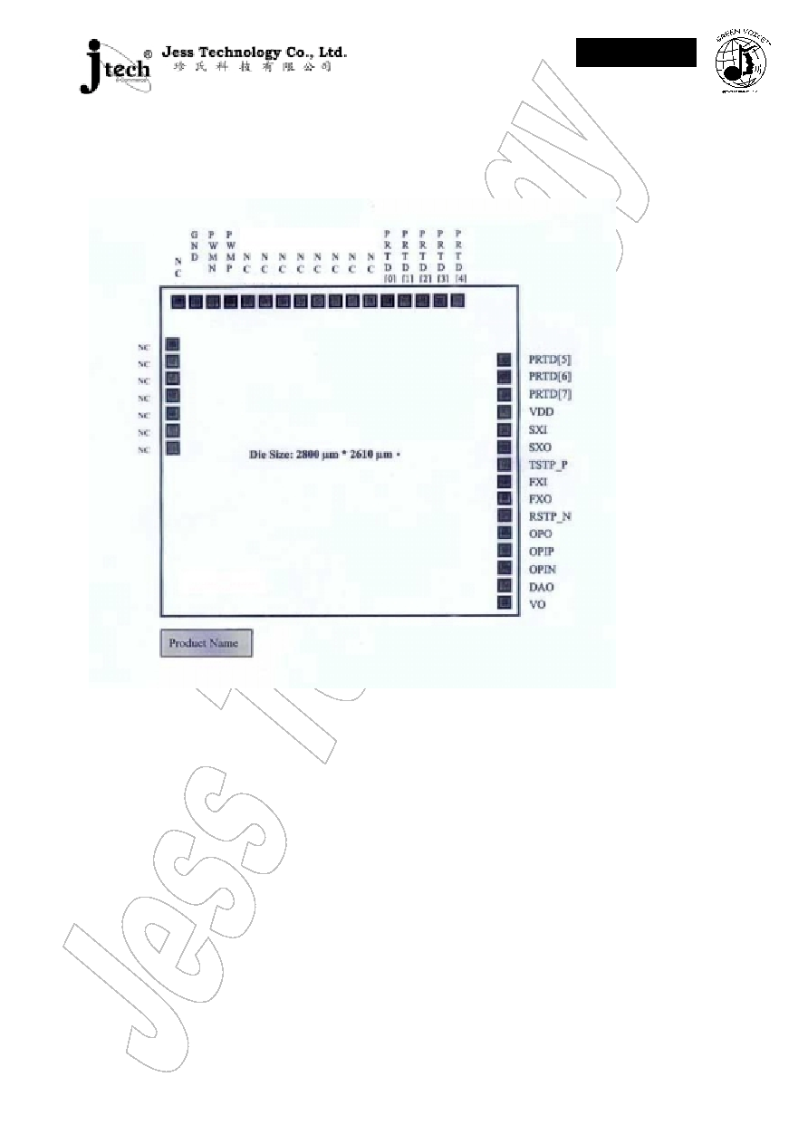
E. Pin Diagram

Suites 2202-7, Tower 6, The Gateway,
9 Canton Road, Tsimshatsui,
Kowloon, Hong Kong
Tel: (852) 2123 3289 Fax: (852) 2123 3393
E-mail: sales@jesstech.com
Home Page: www.jesstech.com
HE80085S
HE80000 SERIES
25 APR 2002
4 OF 8
V1.4
F. Bonding Pad Location
PIN
Number
PIN
Name
X
Coordinate
Y
Coordinate
PIN
Number
PIN
Name
X
Coordinate
Y
Coordinate
1
NC
X= -1312.20 Y= 870.50
21
PRTD[6]
X= 1313.10 Y= 622.40
2
NC
X= -1312.20 Y= 733.60
22
PRTD[5]
X= 1313.10 Y= 759.40
3
NC
X= -1312.20 Y= 596.60
23
PRTD[4]
X= 960.70
Y= 1217.60
4
NC
X= -1312.20 Y= 459.70
24
PRTD[3]
X= 823.80
Y= 1217.60
5
NC
X= -1312.20 Y= 322.80
25
PRTD[2]
X= 686.80
Y= 1217.60
6
NC
X= -1312.20 Y= 185.80
26
PRTD[1]
X= 549.90
Y= 1217.60
7
NC
X= -1312.20 Y= 48.90
27
PRTD[0]
X= 412.90
Y= 1217.60
8
VO
X= 1312.40 Y= -1181.00
28
NC
X= 275.90
Y= 1217.60
9
DAO
X= 1312.40 Y= -1029.20
29
NC
X= 139.00
Y= 1217.60
10
OPIN
X= 1313.10 Y= -884.00
30
NC
X= 2.00
Y= 1217.60
11
OPIP
X= 1313.10 Y= -747.10
31
NC
X= -134.90
Y= 1217.60
12
OPO
X= 1313.10 Y= -610.10
32
NC
X= -271.90
Y= 1217.60
13
RSTP_N
X= 1313.10 Y= -473.20
33
NC
X= -408.80
Y= 1217.60
14
FXO
X= 1313.10 Y= -336.20
34
NC
X= -545.80
Y= 1217.60
15
FXI
X= 1313.10 Y= -199.30
35
NC
X= -682.70
Y= 1217.60
16
TSTP_P
X= 1313.10 Y= -62.40
36
PWMP
X= -832.50
Y= 1217.60
17
SXO
X= 1313.10 Y= 74.60
37
PWMN
X= -995.80
Y= 1217.60
18
SXI
X= 1313.10 Y= 211.60
38
GND
X= -1146.30 Y= 1217.60
19
VDD
X= 1313.10 Y= 348.50
39
NC
X= -1283.30 Y= 1217.60
20
PRTD[7]
X= 1313.10 Y= 485.40
Suites 2202-7, Tower 6, The Gateway,
9 Canton Road, Tsimshatsui,
Kowloon, Hong Kong
Tel: (852) 2123 3289 Fax: (852) 2123 3393
E-mail: sales@jesstech.com
Home Page: www.jesstech.com
HE80085S
HE80000 SERIES
25 APR 2002
5 OF 8
V1.4
G. Electrical Characteristics
Absolute Maximum Rating
Item
Sym.
Rating
Condition
Supply Voltage
V
dd
-0.5V ~ 8V
Input Voltage
V
in
-0.5V ~ V
dd
+0.5V
Output Voltage
V
o
-0.5V ~ V
dd
+0.5V
Operating Temperature
T
op
0
0
C ~ 70
0
C
Storage Temperature
T
st
-50
0
C ~ 100
0
C
Recommended Operating Conditions
Item
Sym.
Rating
Condition
Supply Voltage
V
dd
2.4V ~ 5.2V
V
ih
0.9 V
dd
~ V
dd
Input Voltage
V
il
0.0V ~ 0.1V
dd
8MHz
V
dd
=5.0V
Operating Frequency
Fmax
4MHz
V
dd
=2.4V
Operating Temperature
T
op
0
0
C ~ 70
0
C
Storage Temperature
T
st
-50
0
C ~ 100
0
C

Suites 2202-7, Tower 6, The Gateway,
9 Canton Road, Tsimshatsui,
Kowloon, Hong Kong
Tel: (852) 2123 3289 Fax: (852) 2123 3393
E-mail: sales@jesstech.com
Home Page: www.jesstech.com
HE80085S
HE80000 SERIES
25 APR 2002
6 OF 8
V1.4
Test condition:TEMP=25, VDD=3V+/-10%, GND=0V
PARAMETER
CONDITION
MIN TYP MA
X
UNIT
I
Fast
NORMAL Mode Current System
2M ext. R/C
0.75
1
mA
I
Slow
SLOW Mode Current
System
32.768K X'tal
6
9
A
I
Idle
IDLE Mode Current
System
32.769K X'tal
4
7
A
I
Sleep
Sleep Mode Current
System
1
A
I
oHPW
M
PWM
Output Drive Current
PWMP, PWMN
*2
V
DD
=3V; V
oh
=2V
12
15
mA
I
oLPW
M
PWM
Output Sink Current
PWMP, PWMN
*2
V
DD
=3V; V
oL
=1V
33
40
mA
I
oVO
DAC Output Current
VO, DAO
V
DD
=3V;VO=0~2V,Data=
7F
2.5
3
mA
V
iH
Input High Voltage
I/O pins
0.8
V
DD
V
V
iL
Input Low Voltage
I/O pins
0.2
V
DD
V
V
hys
Input Hysteresis Width
I/O, RSTP_N
Threshold=2/3V
DD
(input
from low to high)
Threshold=1/3V
DD
(input
from high to low)
1/3
V
DD
V
I
oH
Output Drive Current
I/O pull-high
*1
V
oL
=2.0V
50
A
I
oL 1
Output Sink Current
I/O pull-low
*1
V
oL
=0.4V
1.0
mA
I
iL_1
Input Low Current
RSTP_N
V
iL
=GND, pull high
Internally
20
A
I
iL_2
Input Low Current
I/O
V
iL
=GND, if pull high
Internally by user
100
A
Note:
*1: Drive Current Spec. for Push-Pull I/O port only
Sink Current Spec. for both Push-Pull and Open-Drain I/O port.
*2: This Spec. base on one driver only. There are five build-in driver, so user just
multiply the number of driver he used to one driver current
to get the total amount of current.( I
oHPWM
I
oLPWM
* N; N=0,1,2,3,4,5)

Suites 2202-7, Tower 6, The Gateway,
9 Canton Road, Tsimshatsui,
Kowloon, Hong Kong
Tel: (852) 2123 3289 Fax: (852) 2123 3393
E-mail: sales@jesstech.com
Home Page: www.jesstech.com
HE80085S
HE80000 SERIES
25 APR 2002
7 OF 8
V1.4
H. Application Circuit
I. Important Note
For accessing any address large than 64KB, users must update TPP first, TPH then TPL. Only by
this order, the pre-charge circuit of ROM will work correctly. 5us waiting is necessary before LDV
instruction is executed since Data ROM is a low speed ROM. Users can not emulate this
accessing process in ICE. So 5us delay should be added by firmware.
Please bonds the TSTP_P, RSTP_N and PRTD[7:0] with test point on PCB (can be soldered and
probed) as you can, then JESS can do some IC testing job on PCB. Neither VDD nor GND
connection is necessary for TSTP_P. The following figure is an example (Testing point with
through hole.)

Suites 2202-7, Tower 6, The Gateway,
9 Canton Road, Tsimshatsui,
Kowloon, Hong Kong
Tel: (852) 2123 3289 Fax: (852) 2123 3393
E-mail: sales@jesstech.com
Home Page: www.jesstech.com
HE80085S
HE80000 SERIES
25 APR 2002
8 OF 8
V1.4
SUPPLEMENTARY SPECIFICATION :
HE80 Series PWM application
Description:
For HE80 PWM application, the following points must be bare in mind.
1.
The PWM output can direct drive buzzer.
2.
For direct drive speaker, it must use 32
or above speaker.
3.
For speaker application, it must add capacitors between IC's VDD ground and its PWM
output, see below figure.
Note: the 1uF capacitor must be connected near IC's