 | –≠–ª–µ–∫—Ç—Ä–æ–Ω–Ω—ã–π –∫–æ–º–ø–æ–Ω–µ–Ω—Ç: HE831301 | –°–∫–∞—á–∞—Ç—å:  PDF PDF  ZIP ZIP |

Suites 2202-7, Tower 6, The Gateway,
9 Canton Road, Tsimshatsui,
Kowloon, Hong Kong
Tel: (852) 2123 3289 Fax: (852) 2123 3393
E-mail: sales@jesstech.com
Home Page: www.jesstech.com
HE831301
HE80000 SERIES
01 Apr 2002
1 of 11
Preliminary V1.0
A. HE831301 Introduction
HE831301 is a member of 8-bit Micro-controller series that is developed by JESS. Users can
chose any one of combination among 640 dots LCD Driver + 12 Bit I/O Port...256 dots
LCD Driver + 36 Bit I/O Portetc. (Decide by Mask Option). This IC has built-in one OP
comparator. The built-in OP comparator can be used with (lightvoicetemperaturehumility)
sensor. The 7-bit current-type D/A converter and PWM device provide the complete speech
output mechanism. The 64K ROM Size can storage around 20 second's speech. This IC is
applicable to the medium systems such as LCD Games and Educational Toy etc. Use external
SRAM or Flash RAM to have recording function. This IC is applicable to the medium systems
such as LCD Games, Education Toy etc. This IC is very easy to learn and use. Most of
instructions take only 3 oscillator clocks (machine cycles). As a result this IC is suitable for the
applications that require higher performance system.
B. HE831301 Features
Operation Voltage
2.4V ≠ 5.2V
System Clock
DC ~ 8MHz @ 5.0V
DC ~ 4MHz @ 2.4V
Internal ROM
64K Bytes(64K Program ROM)
Internal RAM
512 Bytes
Dual Clock System Normal (Fast) clock 32.768K ~ 8MHz
Slow
clock 32.768KHz
Operation Mode
DUALFASTSLOWIDLESLEEP Mode.
With WDT (WATCH DOG TIMER) to prevent deadlock condition.
12-bit ~ 36-bit Bi-directional I/O port.
Mask Option can select PUSH-PULL or OPEN
DRAIN output mode for each I/O pin.
One built-in OP comparator.
640 ~256 dots LCD driver (AB TYPE selectable).
One 7-bit current-type DAC output.
PWM device.
Two external interrupts and two internal timers interrupts.
Two 16-bit timers.
Instruction set 32 instructions, 4 addressing mode. 9-bit DATA POINTER for RAM and
16-bit TABLE POINTER for ROM.
C. Internal Block
This IC is applicable to the medium systems such as LCD Games, Education Toy etc.
Suites 2202-7, Tower 6, The Gateway,
9 Canton Road, Tsimshatsui,
Kowloon, Hong Kong
Tel: (852) 2123 3289 Fax: (852) 2123 3393
E-mail: sales@jesstech.com
Home Page: www.jesstech.com
HE831301
HE80000 SERIES
01 Apr 2002
2 of 11
Preliminary V1.0
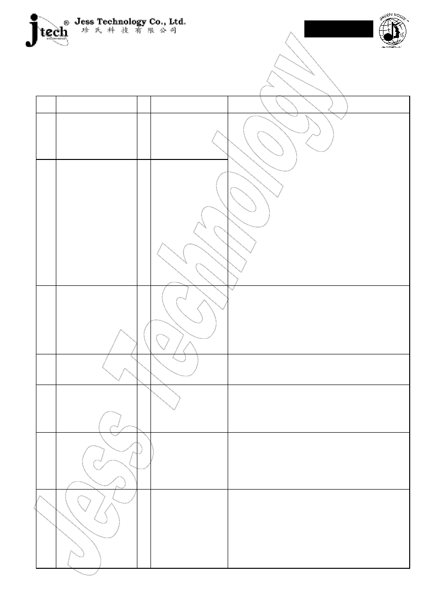
D. Pin Assignment
Pin#
Pin Name
I/O
Function
Description
78
77
FXI,
FXO
B,
O
External fast clock pin.
Connecting to crystal
or RC to generate
32.768 kHz ~ 8MHz
system clock.
81
80
SXI,
SXO
I,
O
External slow clock
pin. Connecting with
32.768 Hz OSC to
generate the stable
frequency for Slow
Clock Mode and Timer
clock source.
Mask Option settings
MO_FCK/SCKN=00Slow Clock only
01Illegal
10Dual Clock
11Fast Clock only
MO_FOSCE=0Internal fast oscillation
1 External fast oscillation
MO_FXTAL=0R,C oscillation for Fast Clock
1Crystal oscillation for Fast Clock
MO_SXTAL=0R,C oscillation for 32.768K Clock
1 Crystal oscillation for 32.768K
Clock
Program the value of OP1and OP2 to change the
operating modes (Normal, Slow, Idle and Sleep).
In Dual Clock mode , the system runs in Fast Clock,
only the LCD and timer I use the 32.768K clock
source
76
RSTP_N
I System reset signal
Pull this pin to low level to reset the system. Besides,
select the Mask Option (MQ_PORE=1) to enable the
HE831301 internal Power-on Reset function.
In addition, the MO_WDTE is used for Watch
Timer setting
MO_WDTE=0Disable Watch Dog Timer
=1Enable Watch Dog Timer
79
TSTP_P
I
Test Pin
Please bond this pin and add a test point on PCB
for debugging. But for improving ESD, please
connect this pin with zero Ohm resistor to GND.
91,
92,
93,
1
PRTC[3:0]
B
Port C bi-directional
I/O Pin (4Pins)
Mask Option MO_CPP[3:0] to preset the output type
MO_CPP=1 : Push-pull output;
=0 : Open-drain output
When assigned the port to input pin, send a '1' and read
the result to get the input value
83..
90
PRTD[7:0]
B
Port D bi-directional
I/O pin (8 pins).
PRTD[7:2] is also a
Wake-up pin and
PRTD[7:6] is used for
interrupt input pin.
Mask Option MO_DPP[7:0] to preset the output type
MO_DPP= 1: Push-pull output;
= 0: Open-drain output
When assigned the port to input pin, send a '1' and read
the result to get the input value
12..
19
PRT17[7:0]/SEG[39:32]
B/
O
Port 17 bi-directional
pin(8pins) or LCD
Segment[39:32]
Mask Option MO_LIO17[7:0]
Set 8 pins to be I/O or LCD Segment:
MO_LIO17[7:0]=0I/O Pin
=1LCD Pin
I/O Pin Assigned
Mask Option MO_17PP[7:0]
MO_17PP[7:0]=0Open-drain output
=1Push-pull output

Suites 2202-7, Tower 6, The Gateway,
9 Canton Road, Tsimshatsui,
Kowloon, Hong Kong
Tel: (852) 2123 3289 Fax: (852) 2123 3393
E-mail: sales@jesstech.com
Home Page: www.jesstech.com
HE831301
HE80000 SERIES
01 Apr 2002
3 of 11
Preliminary V1.0
20..
27
PRT15[7:0]/SEG[31:24]
B/
O
Port 15 bi-directional
pin(8pins) or LCD
Segment[31:24]
Mask Option MO_LIO15[7:0]
Set 8 pins to be I/O or LCD Segment:
MO_LIO15[7:0]=0I/O Pin
=1LCD Pin
I/O Pin Assigned
Mask Option MO_15PP[7:0]
MO_15PP[7:0]=0Open-drain output
=1Push-pull output
28..
35
PRT14[7:0]/
SEG[23:16]
B/
O
Port 14 bi-directional
pin(8pins) or LCD
Segment[23:16]
Mask Option MO_LIO14[7:0]
Set 8 pins to be I/O or LCD Segment
MO_LIO14[7:0]=0I/O Pin
=1LCD Pin
I/O Pin Assigned
Mask Option MO_14PP[7:0]
MO_14PP[7:0]= 0Open-drain output
= 1Push-pull output
11..4
52..59
COM[15:0]
O LCD COMmon Output
36..51
SEG[15:0]
O LCD SEGment Output
Data filled from D8H, please refer the LCD RAM Map
61
LC2
B Charge Pump Switch 1
60
LC1
B Charge Pump Switch 2
LV3=VDD
Charge Pump for LCD is turn off. Take one
0.1 µF capacitor between LC1 and LC2 off. Please
refer the application circuit in order to avoid power
consumption.
63
LV3
B Charge Pump V3
62
LV1
B Charge Pump V1
Please refer the application circuit.
64..68
LR[4..0]
B
LCD Resister level 4 ~
0
Please refer the application circuit.
69
LVG
I LCD Virtual Ground
Please refer the application circuit
2
PWMP
O
PWM +ve output pin
can directly drive
Speaker or Buzzer
for sound output.
Set the Bit2 for VOC register (PWM =1) to turn on the
PWM
3
PWMN
O
PWM -ve output pin
can directly drive
Speaker or Buzzer for
sound output.
Set the Bit2 for VOC register (PWM =1) to turn on the
PWM
71
VO
O D/A voice output
Set the bit1 (DA=1) of VOC register to turn on VO
72
DAO
O
D/A voice output for OP
use.
Set the bit0 (OP=1) of VOC register to turn on DAO
73
OPIN
I OPAMP Inverting pin
74
OPIP
I
OPAMP Non-Inverting
pin
75
OPO
O OPAMP Output pin
Set the bit1 (OP=1) register to turn on OP
Individual Op comparator
82
VDD
P Positive Power Input
70
GND
P Power Ground Input
Adding 0.1 µF capacitor as by-pass capacitor on power
pins is necessary.(within 1 cm distance)

Suites 2202-7, Tower 6, The Gateway,
9 Canton Road, Tsimshatsui,
Kowloon, Hong Kong
Tel: (852) 2123 3289 Fax: (852) 2123 3393
E-mail: sales@jesstech.com
Home Page: www.jesstech.com
HE831301
HE80000 SERIES
01 Apr 2002
4 of 11
Preliminary V1.0
E.LCD RAM Map
Page
0
SEG
[7:0]
SEG
[15:8]
SEG
[23:16]
SEG
[31:24]
SEG
[39:32]
COM0
80H
90H
A0H
B0H
C0H
COM1
81H
91H
A1H
B1H
C1H
COM2
82H
92H
A2H
B2H
C2H
:
:
:
:
:
:
:
:
:
:
:
:
COM13
8DH
9DH
ADH
BDH
CDH
COM14
8EH
9EH
AEH
BEH
CEH
COM15
8FH
9FH
AFH
BFH
CFH

Suites 2202-7, Tower 6, The Gateway,
9 Canton Road, Tsimshatsui,
Kowloon, Hong Kong
Tel: (852) 2123 3289 Fax: (852) 2123 3393
E-mail: sales@jesstech.com
Home Page: www.jesstech.com
HE831301
HE80000 SERIES
01 Apr 2002
5 of 11
Preliminary V1.0
F . Pin Diagram
Product name
Die Size: 3100 µm * 3240 µm
Substrate connect with GND
P
R
T
C
[1]
P
R
T
C
[2]
P
R
T
C
[3]
P
R
T
D
[0]
P
R
T
D
[1]
P
R
T
D
[2]
P
R
T
D
[3]
P
R
T
D
[4]
P
R
T
D
[5]
P
R
T
D
[6]
P
R
T
D
[7]
V
D
D
S
X
I
S
X
O
T
S
T
P
|
P
F
X
I
F
X
O
R
S
T
P
|
N
O
P
O
O
P
I
P
O
P
I
N
D
A
O
VO
GND
LVG
LR0
LR1
LR2
LR3
LR4
LV3
LV1
LC2
LC1
COM[0]
COM[1]
COM[2]
COM[3]
COM[4]
COM[5]
COM[6]
COM[7]
SEG[0]
SEG[1]
SEG[2]
SEG[3]
SEG[4]
SEG[5]
PRTC[0]
PWMP
PWMN
COM[8]
COM[9]
COM[10]
COM[11]
COM[12]
COM[13]
COM[14]
COM[15]
SEG[39]
SEG[38]
SEG[37]
SEG[36]
SEG[35]
SEG[34]
SEG[33]
SEG[32]
SEG[31]
SEG[30]
SEG[29]
SEG[28]
SEG[27]
S
E
G
[26]
S
E
G
[25]
S
E
G
[24]
S
E
G
[23]
S
E
G
[22]
S
E
G
[21]
S
E
G
[20]
S
E
G
[19]
S
E
G
[18]
S
E
G
[17]
S
E
G
[16]
S
E
G
[15]
S
E
G
[14]
S
E
G
[13]
S
E
G
[12]
S
E
G
[11]
S
E
G
[10]
S
E
G
[9]
S
E
G
[8]
S
E
G
[7]
S
E
G
[6]