 | –≠–ª–µ–∫—Ç—Ä–æ–Ω–Ω—ã–π –∫–æ–º–ø–æ–Ω–µ–Ω—Ç: HE83133 | –°–∫–∞—á–∞—Ç—å:  PDF PDF  ZIP ZIP |

Suites 2202-7, Tower 6, The Gateway,
9 Canton Road, Tsimshatsui,
Kowloon, Hong Kong
Tel: (852) 2123 3289 Fax: (852) 2123 3393
E-mail: sales@jesstech.com
Home Page: www.jesstech.com
HE83133
HE80000 SERIES
25 APR 2002
1 of 10
V1.0
A.HE83133 Introduction
HE83133 is a member of Jess Tech HE8000 series 8-bit CMOS micro-controller. This IC can
share the LCD pin and I/O pin (From 640-dot of LCD driver + 12 Bit I/O Port ... 320-dot of
LCD driver + 32 Bit I/O Port), the combination of the above is selected by Mask Option. It built-
in one internal Op-Amp, one 7-bit D/A converter and one PWM output module to provide a
speech output interface. Use the built-in 384K ROM can store around 120 seconds of speech data.
In addition, it can be connected with external SRAM or Flash RAM for recording function.
The HE83133 provides a very simple and effective instruction set, each instruction byte occupies
only 1.5 clock cycle time, therefore, it is suitable to apply in the high performance systems.
B.HE83133 Features
!
Operating Voltage:
2.4V ≠ 5.2V
!
Operation frequency Range:
DC ~ 8MHz @ 5.0V
DC ~ 4MHz @ 2.4V
!
ROM size:
384K Bytes
!
RAM size:
256 Bytes
!
Dual Clock:
Normal(Fast) clock:
32.768K ~ 8MHz
Slow
clock:
32.768KHz
!
Operating Mode:
DUAL FASTSLOWIDLESLEEP
!
Built-in WATCH DOG TIMER
!
12~32 bi-directional I/O pins, PUSH-PULL or OPEN DRAIN output selected by mask option
!
Built-in an internal Op-Amp
!
320~640 LCD driver (AB TYPE)
!
Built-in one 7-bit D/A Converter
!
Built-in a PWM output circuit
!
Provides two internal and two external interrupt
!
Provides two 16-bit timer (no time base)
!
Instruction Set : 32 Instructions, 4 types of Addressing Mode, 2 individual Pointer for ROM
(19-bit) and RAM (8-bit) table access.
C.HE83133 Application
!
Interface to Light, Sound, Temperature and Humidity sensor for controlling application.
!
Suitable in LCD games, education toys, and some mid-end electronic products.
!
Interface to external SRAM or Flash RAM for recording function.

Suites 2202-7, Tower 6, The Gateway,
9 Canton Road, Tsimshatsui,
Kowloon, Hong Kong
Tel: (852) 2123 3289 Fax: (852) 2123 3393
E-mail: sales@jesstech.com
Home Page: www.jesstech.com
HE83133
HE80000 SERIES
25 APR 2002
2 of 10
V1.0
D. Pin Assignment
Pin
Pin Name
I/O
Function
Description
77
76
FXI,
FXO
B,
O
External Fast Clock pin. To
connect the Crystal or R,C
oscillation to generate
32.768KHz ~ 8MHz
system clock.
80
79
SXI,
SXO
I,
O
External Slow Clock pin .
To connect the 32.768KHz
oscillator to generate the
stable frequency for Slow
Mode, and provide IC LCD
display, Timer clock
source.
Mask Option settings :
MO_FCK/SCKN=00Slow Clock only
01Illegal
10Dual Clock
11Fast Clock only
MO_FOSCE=0Internal fast oscillation
1External fast oscillation
MO_FXTAL=0R,C oscillation for Fast Clock
1Crystal oscillation for Fast Clock
MO_SXTAL=0R,C oscillation for 32.768K Clock
1X'tal oscillation for 32.768K Clock
Program the value of OP1and OP2 to change the
operating modes (NormalSlowIdle and Sleep).
In Dual Clock modethe system runs in Fast Clock, only
the Timer 1 use the 32.768K clock source.
75
RSTP_N
I
System reset signal
Pull this pin to low level to reset the system. Besides,
Select the Mask Option (MO_PORE=1) to enable the IC
internal Power-on Reset function.
In addition, the MO_WDTE is used for Watch Dog
Timer setting
MO_WDTE =0Disable Watch Dog Timer
=1Enable Watch Dog Timer
78
TSTP_P
I
Test Pin.
Please bond this pin and add a test point on PCB for
debugging. Leave this pin floating is OK.
90..
92,
1
PRTC[3:0]
B
Port C bi-directional I/O
pin (4 pins).
Mask Option MO_CPP[3:0] to preset the output type:
MO_CPP=1 : Push-pull output
= 0 : Open-drain output.
When assigned the port to input pin, send a `1' and read
the result to get the input value.
82..
89
PRTD[7:0]
B
Port D bi-directional I/O
pin, (8 pins). PRTD[7:2] is
also a Wake-up pin and
PRTD[7:6] is used for
interrupt input pin.
Mask Option MO_DPP[7:0] to preset the output type:
MO_DPP=1 : Push-pull output
0 : Open-drain output
When assigned the port to input pin, send a `1' and read
the result to get the input value.
12..
15
PRT17[7:4]/
SEG[39:36]
B/
O
Port 17 bi-directional I/O
pin, total 4 pin or LCD
Segment[39:36]
Mask Option MO_LIO17[7:4] to set the 4 pin to I/O or
LCD Segment
MO_LIO17[7:0]=0I/O Pin=1LCD Pin
When use for I/O Pin,
Mask Option MO_17PP[7:4] can use to set the output
status:
MO_17PP[7:4]=0Open-drain output
=1Push-pull output
Suites 2202-7, Tower 6, The Gateway,
9 Canton Road, Tsimshatsui,
Kowloon, Hong Kong
Tel: (852) 2123 3289 Fax: (852) 2123 3393
E-mail: sales@jesstech.com
Home Page: www.jesstech.com
HE83133
HE80000 SERIES
25 APR 2002
3 of 10
V1.0
16..
23
PRT15[7:0]/
SEG[35:28]
B/
O
Port 15 bi-directional I/O
pin, total 8 pin or LCD
Segment[35:28]
Mask Option MO_LIO15[7:0] to set the 8 pin to I/O or
LCD Segment
MO_LIO15[7:0]=0I/O Pin=1LCD Pin
When use for I/O Pin,
Mask Option MO_15PP[7:0] can use to set the output
status:
MO_15PP[7:0]=0Open-drain output
=1Push-pull output
24..
31
PRT14[7:0]/
SEG[27:20]
B/
O
Port 14 bi-directional I/O
pin, total 8 pin or LCD
Segment[27:20]
Mask Option MO_LIO14[7:0] to set the 8 pin to I/O or
LCD Segment
MO_LIO14[7:0]=0I/O Pin=1LCD Pin
When use for I/O Pin,
Mask Option MO_14PP[7:0] can use to set the output
status:
MO_14PP[7:0]=0Open-drain output
=1Push-pull output
11..4
52..
59
COM[15:0] O
LCD COMmon Output
32..
51
SEG[19:0]
O
LCD SEGment Output
Fill the data from 80H, refer LCD and RAM map.
61
LC2
B
Charge Pump Switch 1
60
LC1
B
Charge Pump Switch 2
Refer to application circuit.
63
LV3
B
Charge Pump V3
62
LV1
B
Charge Pump V1
Refer to application circuit.
64..
67
LR[4..1]
B
LCD Resister level 4 ~ 1
Refer to application circuit.
68
LVG
I
LCD Virtual Ground
Refer to application circuit.
2
PWMP
O
PWM +ve O/P pin, can
directly drive Speaker or
Buzzer for voice output.
Preset the Bit2 of VOC register: PWM =1turn on
PWM.
3
PWMN
O
PWM -ve O/P pin, can
directly drive Speaker or
Buzzer for voice output.
Preset the Bit2 of VOC register: PWM =1turn on
PWM.
70
VO
O
D/A voice output
Preset the Bit-1 of VOC register: DA=1turn on VO.
71
DAO
O
D/A voice output, for OP
use
Preset the Bit-0 of VOC register: OP=1turn on DAO.
72
OPIN
I
OPAMP Inverting I/P pin
73
OPIP
I
OPAMP Non-inverting I/P
pin.
74
OPO
O
OPAMP O/P pin
Individual built-in OP-Amp
81
VDD
P
Positive Power Input
69
GND
P
Power Ground Input
Adding 0.1mF capacitor as by-pass capacitor is between
VDD and GND is necessary

Suites 2202-7, Tower 6, The Gateway,
9 Canton Road, Tsimshatsui,
Kowloon, Hong Kong
Tel: (852) 2123 3289 Fax: (852) 2123 3393
E-mail: sales@jesstech.com
Home Page: www.jesstech.com
HE83133
HE80000 SERIES
25 APR 2002
4 of 10
V1.0
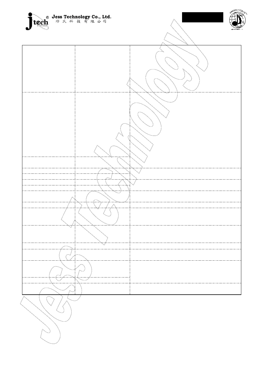
E. LCD RAM Map
Page
0
SEG
[7:0]
SEG
[15:8]
SEG
[23:16]
SEG
[31:24]
SEG
[39:32]
COM0
80H
90H
A0H
B0H
C0H
COM1
81H
91H
A1H
B1H
C1H
COM2
82H
92H
A2H
B2H
C2H
:
:
:
:
:
:
:
:
:
:
:
:
COM13
8DH
9DH
ADH
BDH
CDH
COM14
8EH
9EH
AEH
BEH
CEH
COM15
8FH
9FH
AFH
BFH
CFH
F. Pin Diagram
Suites 2202-7, Tower 6, The Gateway,
9 Canton Road, Tsimshatsui,
Kowloon, Hong Kong
Tel: (852) 2123 3289 Fax: (852) 2123 3393
E-mail: sales@jesstech.com
Home Page: www.jesstech.com
HE83133
HE80000 SERIES
25 APR 2002
5 of 10
V1.0
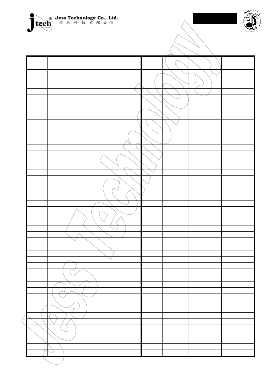
G. Bonding Pad Location
PIN
Number
PIN
Name
X
Coordinate
Y
Coordinate
PIN
Number
PIN
Name
X
Coordinate
Y
Coordinate
1
PRTC[0]
X= -1011.00
Y= 1635.10
47
SEG[4]
X= 1025.00 Y= -1636.50
2
PWMP
X= -1820.20 Y= 1287.70
48
SEG[3]
X= 1140.50 Y= -1636.50
3
PWMN
X= -1820.20 Y= 1124.30
49
SEG[2]
X= 1256.00 Y= -1636.50
4
COM[8]
X= -1820.20 Y= 985.20
50
SEG[1]
X= 1371.50 Y= -1636.50
5
COM[9]
X= -1820.20 Y= 869.80
51
SEG[0]
X= 1487.00 Y= -1636.50
6
COM[10]
X= -1820.20 Y= 754.20
52
COM[7]
X= 1818.30 Y= -1535.20
7
COM[11]
X= -1820.20 Y= 638.80
53
COM[6]
X= 1818.30 Y= -1419.80
8
COM[12]
X= -1820.20 Y= 523.20
54
COM[5]
X= 1818.30 Y= -1304.20
9
COM[13]
X= -1820.20 Y= 407.80
55
COM[4]
X= 1818.30 Y= -1188.80
10
COM[14]
X= -1820.20 Y= 292.20
56
COM[3]
X= 1818.30 Y= -1073.20
11
COM[15]
X= -1820.20 Y= 176.80
57
COM[2]
X= 1818.30 Y= -957.80
12
PRT17[7]
X= -1820.20 Y= 61.20
58
COM[1]
X= 1818.30 Y= -842.20
13
PRT17[6]
X= -1820.20 Y= -54.20
59
COM[0]
X= 1818.30 Y= -726.80
14
PRT17[5]
X= -1820.20 Y= -169.80
60
LC1
X= 1818.30 Y= -611.20
15
PRT17[4]
X= -1820.20 Y= -285.20
61
LC2
X= 1818.30 Y= -495.80
16
PRT15[7]
X= -1820.20 Y= -400.80
62
LV1
X= 1818.30 Y= -380.20
17
PRT15[6]
X= -1820.20 Y= -516.20
63
LV3
X= 1818.30 Y= -264.80
18
PRT15[5]
X= -1820.20 Y= -631.80
64
LR4
X= 1818.30 Y= -149.20
19
PRT15[4]
X= -1820.20 Y= -747.20
65
LR3
X= 1818.30 Y= -33.80
20
PRT15[3]
X= -1820.20 Y= -862.80
66
LR2
X= 1818.30 Y= 81.80
21
PRT15[2]
X= -1820.20 Y= -978.20
67
LR1
X= 1818.30 Y= 197.20
22
PRT15[1]
X= -1820.20 Y= -1093.80
68
LVG
X= 1818.30 Y= 312.80
23
PRT15[0]
X= -1747.00 Y= -1636.50
69
GND
X= 1818.30 Y= 428.20
24
PRT14[7]
X= -1631.50 Y= -1636.50
70
VO
X= 1699.90 Y= 1634.40
25
PRT14[6]
X= -1516.00 Y= -1636.50
71
DAO
X= 1548.10 Y= 1634.40
26
PRT14[5]
X= -1400.50 Y= -1636.50
72
OPIN
X= 1414.50 Y= 1635.10
27
PRT14[4]
X= -1285.00 Y= -1636.50
73
OPIP
X= 1299.00 Y= 1635.10
28
PRT14[3]
X= -1169.50
Y= -1636.50
74
OPO
X= 1183.50 Y= 1635.10
29
PRT14[2]
X= -1054.00 Y= -1636.50
75
RSTP_N
X= 1068.00 Y= 1635.10
30
PRT14[1]
X= -938.50 Y= -1636.50
76
FXO
X= 952.50 Y= 1635.10
31
PRT14[0]
X= -823.00 Y= -1636.50
77
FXI
X= 837.00 Y= 1635.10
32
SEG[19]
X= -707.50 Y= -1636.50
78
TSTP_P
X= 721.50 Y= 1635.10
33
SEG[18]
X= -592.00 Y= -1636.50
79
SXO
X= 606.00 Y= 1635.10
34
SEG[17]
X= -476.60 Y= -1636.50
80
SXI
X= 490.40 Y= 1635.10
35
SEG[16]
X= -361.10 Y= -1636.50
81
VDD
X= 374.90 Y= 1635.10
36
SEG[15]
X= -245.60 Y= -1636.50
82
PRTD[7]
X= 259.40 Y= 1635.10
37
SEG[14]
X= -130.10 Y= -1636.50
83
PRTD[6]
X= 143.90 Y= 1635.10
38
SEG[13]
X= -14.60 Y= -1636.50
84
PRTD[5]
X= 28.40 Y= 1635.10
39
SEG[12]
X= 101.00 Y= -1636.50
85
PRTD[4]
X= -87.10 Y= 1635.10
40
SEG[11]
X= 216.40 Y= -1636.50
86
PRTD[3]
X= -202.60 Y= 1635.10
41
SEG[10]
X= 331.90 Y= -1636.50
87
PRTD[2]
X= -318.10 Y= 1635.10
42
SEG[9]
X= 447.40 Y= -1636.50
88
PRTD[1]
X= -433.60 Y= 1635.10
43
SEG[8]
X= 563.00 Y= -1636.50
89
PRTD[0]
X= -549.10 Y= 1635.10
44
SEG[7]
X= 678.50 Y= -1636.50
90
PRTC[3]
X= -664.60 Y= 1635.10
45
SEG[6]
X= 794.00 Y= -1636.50
91
PRTC[2]
X= -780.10 Y= 1635.10
46
SEG[5]
X= 909.50 Y= -1636.50
92
PRTC[1]
X= -895.60 Y= 1635.10