 | –≠–ª–µ–∫—Ç—Ä–æ–Ω–Ω—ã–π –∫–æ–º–ø–æ–Ω–µ–Ω—Ç: HE83146 | –°–∫–∞—á–∞—Ç—å:  PDF PDF  ZIP ZIP |

Suites 2202-7, Tower 6, The Gateway,
9 Canton Road, Tsimshatsui,
Kowloon, Hong Kong
Tel: (852) 2123 3289 Fax: (852) 2123 3393
E-mail: sales@jesstech.com
Home Page: www.jesstech.com
HE83146
HE80000 SERIES
25 APR 2002
1 of 10
V1.0
A.HE83146 Introduction
HE83146 is a member of Jess Tech HE80000 series 8-bit CMOS micro-controller. This IC can
share the LCD pin and I/O pin (From 1024-dot of LCD driver + 8 Bit I/O Port) ... (768-dot of
LCD driver + 24 Bit I/O Port)etc, The 7-bit current-type D/A converter and PWM device provide
the complete speech output mechanism. The 192K ROM Size can be used in the storage of
speech, graphic, text etc. It can be applicable to the medium systems such as Small-Scale
Dictionary, Data Bank, Pocket Dialer, Educational Toy etc.
The instruction set of HE83146 are quite easy to learn and simple to use. Only about thirty
instructions with four-type addressing mode are provided. Most of instructions take only 3
oscillator clocks (machine cycles). The processing power is enough to most of battery operation
system.
B.HE83146 Features
!
Operating Voltage:
2.4V ≠ 5.2V
!
Operation frequency Range:
DC ~ 8MHz @ 5.0V
DC ~ 4MHz @ 2.4V
!
ROM size:
192K Bytes(64K Program ROM + 128K Data ROM)
!
RAM size:
256 Bytes
!
Dual Clock:
Normal(Fast) clock:
32.768K ~ 8MHz
Slow
clock:
32.768KHz
!
Operating Mode:
DUAL FASTSLOWIDLESLEEP Mode
!
8~24 bit bi-directional I/O port, Mask Option can select PUSH-PULL or OPEN DRAIN output
mode for each I/O pin. 8 of them are shared with LCD segment pins.
!
One built-in OP Comparator.
!
1024~768 dots LCD driver (B TYPE selectable)
!
One 7-bit current-type DAC output.
!
PWM device.
!
Two external interrupts and three internal timer interrupts.
!
Two 16-bit timer and one Time-Base timer.
!
Instruction Set : 32 Instructions, 4 addressing mode. 8-bit DATA POINTER for RAM and 18-
bit TABLE POINTER for ROM.
C.HE83146 Application
!
Applicable to the medium systems such as Small-Scale Dictionary, Data Bank, Pocket Dialer,
Educational Toy, Digital Voice Recording System etc..

Suites 2202-7, Tower 6, The Gateway,
9 Canton Road, Tsimshatsui,
Kowloon, Hong Kong
Tel: (852) 2123 3289 Fax: (852) 2123 3393
E-mail: sales@jesstech.com
Home Page: www.jesstech.com
HE83146
HE80000 SERIES
25 APR 2002
2 of 10
V1.0
D. Pin Assignment
Pin
Pin Name
I/O
Function
Description
92
91
FXI,
FXO
B,
O
External Fast Clock pin.
Connecting to crystal or
RC to generate 32.768KHz
~ 8MHz frequency.
95
94
SXI,
SXO
I,
O
External Slow Clock pin.
Connecting with 32768Hz
crystal or resistor as slow
clock and providing clock
source for LCD display,
TIMER 1, Time-Base and
other internal blocks.
Mask Option settings :
MO_FCK/SCKN=00Slow Clock only
01Illegal
10Dual Clock
11Fast Clock only
MO_FOSCE=0Internal fast oscillation
1External fast oscillation
MO_FXTAL=0R,C oscillation for Fast Clock
1X'tal osc. for Fast Clock
MO_SXTAL=0R,C oscillation for 32768Hz Clock
1X'tal osc. for 32768Hz Clock
Use OP1and OP2 to switch among different operation
mode (NORMAL, SLOW, IDEL and SLEEP). In Dual
Clock modethe main system clock is still the Fast
Clock. The 32768Hz clock is for LCD and timer 1 only.
90
RSTP_N
I
System reset
Level trigger active low. Except for using this pin, using
mask option (MO_PORE=1) could enable IC build-in
Power-on reset circuit.
Besides, MO_WDTE can set Watch Dog Timer :
MO_WDTE =0Disable Watch Dog Timer
=1Enable Watch Dog Timer
93
TSTP_P
I
Test Pin.
Please bond this pin and add a test point on PCB for
debugging. Leave this pin floating is OK.
97..
104
PRTD[7:0]
B
8-pin bi-directional port.
PRTD[7..2] as wake-up
pin.
PRTD[7..6] as external
interrupt pin.
Mask Option
MO_DPP[7:0] =1 : Push-pull
=0 : Open-drain
Output must be "1" before reading whenever use them as
input (No tri-state structure).
5..
12
PRT15[7:0]/
SEG[63:56]
B/
O
8-pin bi-directional I/O port
that is shared with LCD
segment pin.
Mask Option
MO_LIO15[7:0] =1 ~LCD segment pin
=0 ~I/O pin,
MO_15PP[7:0] =1 : Push-pull
0 : Open-drain
Output must be "1" before reading whenever use them as
input (No tri-state structure).
13..
20
PRT14[7:0]/
SEG[55:48]
B/
O
8-pin bi-directional I/O port
that is shared with LCD
segment pin.
Mask Option
MO_LIO14[7:0] =1 ~LCD segment pin
=0 ~I/O pin,
MO_14PP[7:0] =1 : Push-pull
0 : Open-drain
Output must be "1" before reading whenever use them as
input (No tri-state structure).
4..1,
110..
107
69...
76
COM[15:0] O
LCD COMmon Output
21..
68
SEG[47:0]
O
LCD SEGment Output
LCD Data filled from 80H, please refer the LCD RAM
map.

Suites 2202-7, Tower 6, The Gateway,
9 Canton Road, Tsimshatsui,
Kowloon, Hong Kong
Tel: (852) 2123 3289 Fax: (852) 2123 3393
E-mail: sales@jesstech.com
Home Page: www.jesstech.com
HE83146
HE80000 SERIES
25 APR 2002
3 of 10
V1.0
7
8
LC2
B
Charge Pump Switch 1
77
LC1
B
Charge Pump Switch 2
Add one 0.1
µ
F capacitor between LC1 and LC2. Please
refer the application circuit.
81
LV3
B
Charge Pump V3
80
LV2
B
Charge Pump V2
79
LV1
B
Charge Pump V1
V3<9 Volts.
Please refer the application circuit.
82..
86
LR[4..0]
B
LCD Resister level 4 ~ 1
Please refer the application circuit.
87
LVG
I
LCD Virtual Ground
Please refer the application circuit.
105 PWMP
O
The PWM positive output
can drive speaker or buzzer
directly.
Set the bit-2 of VOC register (PWM =1) to turn on the
PWM
106 PWMN
O
PWM negative output can
drive speaker or buzzer
directly.
Set the bit-2 of VOC register (PWM =1) to turn on the
PWM.
89
VO
O
D/A voice output
Set the bit-1 (VO =1) of VOC register to turn on DAC
with VO output.
96
VDD
P
Positive Power Input
88
GND
P
Power Ground Input
Adding 0.1
µ
F capacitor as by-pass capacitor is between
VDD and GND is necessary
E.LCD RAM Map
Page
0
SEG
[7:0]
SEG
[15:8]
SEG
[23:16]
SEG
[31:24]
SEG
[39:32]
SEG
[47:40]
SEG
[55:48]
SEG
[63:56]
COM0
80H
90H
A0H
B0H
C0H
D0H
E0H
F0H
COM1
81H
91H
A1H
B1H
C1H
D1H
E1H
F1H
COM2
82H
92H
A2H
B2H
C2H
D2H
E2H
F2H
:
:
:
:
:
:
:
:
:
:
:
:
:
:
:
:
:
:
COM13
8DH
9DH
ADH
BDH
CDH
DDH
EDH
FDH
COM14
8EH
9EH
AEH
BEH
CEH
DEH
EEH
FEH
COM15
8FH
9FH
AFH
BFH
CFH
DFH
EFH
FFH
Suites 2202-7, Tower 6, The Gateway,
9 Canton Road, Tsimshatsui,
Kowloon, Hong Kong
Tel: (852) 2123 3289 Fax: (852) 2123 3393
E-mail: sales@jesstech.com
Home Page: www.jesstech.com
HE83146
HE80000 SERIES
25 APR 2002
4 of 10
V1.0
F. Pin Diagram

Suites 2202-7, Tower 6, The Gateway,
9 Canton Road, Tsimshatsui,
Kowloon, Hong Kong
Tel: (852) 2123 3289 Fax: (852) 2123 3393
E-mail: sales@jesstech.com
Home Page: www.jesstech.com
HE83146
HE80000 SERIES
25 APR 2002
5 of 10
V1.0
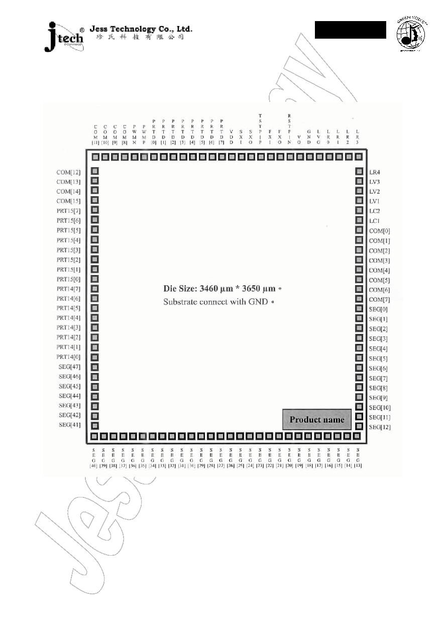
G. Bonding Pad Location
PIN
Number
PIN
Name
X
Coordinate
Y
Coordinate
PIN
Number
PIN
Name
X
Coordinate
Y
Coordinate
1
COM[12] X= -1657.05 Y= 1500.75
56
SEG[12]
X= 1656.70 Y= -1502.25
2
COM[13] X= -1657.05 Y= 1385.25
57
SEG[11]
X= 1656.70 Y= -1386.75
3
COM[14] X= -1657.05 Y= 1269.75
58
SEG[10]
X= 1656.70 Y= -1271.25
4
COM[15] X= -1657.05 Y= 1154.25
59
SEG[9]
X= 1656.70 Y= -1155.75
5
PRT15[7] X= -1657.05 Y= 1038.75
60
SEG[8]
X= 1656.70 Y= -1040.25
6
PRT15[6] X= -1657.05 Y= 923.25
61
SEG[7]
X= 1656.70 Y= -924.75
7
PRT15[5] X= -1657.05 Y= 807.75
62
SEG[6]
X= 1656.70 Y= -809.25
8
PRT15[4] X= -1657.05 Y= 692.25
63
SEG[5]
X= 1656.70 Y= -693.75
9
PRT15[3] X= -1657.05 Y= 576.75
64
SEG[4]
X= 1656.70 Y= -578.25
10
PRT15[2] X= -1657.05 Y= 461.25
65
SEG[3]
X= 1656.70 Y= -462.75
11
PRT15[1] X= -1657.05 Y= 345.75
66
SEG[2]
X= 1656.70 Y= -347.25
12
PRT15[0] X= -1657.05 Y= 230.25
67
SEG[1]
X= 1656.70 Y= -231.75
13
PRT14[7] X= -1657.05 Y= 114.75
68
SEG[0]
X= 1656.70 Y= -116.25
14
PRT14[6] X= -1657.05 Y= -0.75
69
COM[7]
X= 1656.70 Y= -0.75
15
PRT14[5] X= -1657.05 Y= -116.25
70
COM[6]
X= 1656.70 Y= 114.75
16
PRT14[4] X= -1657.05 Y= -231.75
71
COM[5]
X= 1656.70 Y= 230.25
17
PRT14[3] X= -1657.05 Y= -347.25
72
COM[4]
X= 1656.70 Y= 345.75
18
PRT14[2] X= -1657.05 Y= -462.75
73
COM[3]
X= 1656.70 Y= 461.25
19
PRT14[1] X= -1657.05 Y= -578.25
74
COM[2]
X= 1656.70 Y= 576.75
20
PRT14[0] X= -1657.05 Y= -693.75
75
COM[1]
X= 1656.70 Y= 692.25
21
SEG[47]
X= -1657.05 Y= -809.25
76
COM[0]
X= 1656.70 Y= 807.75
22
SEG[46]
X= -1657.05 Y= -924.75
77
LC1
X= 1656.70 Y= 923.25
23
SEG[45]
X= -1657.05 Y= -1040.25
78
LC2
X= 1656.70 Y= 1038.75
24
SEG[44]
X= -1657.05 Y= -1155.75
79
LV1
X= 1656.70 Y= 1154.25
25
SEG[43]
X= -1657.05 Y= -1271.25
80
LV2
X= 1656.70 Y= 1269.75
26
SEG[42]
X= -1657.05 Y= -1386.75
81
LV3
X= 1656.70 Y= 1385.25
27
SEG[41]
X= -1657.05 Y= -1502.25
82
LR4
X= 1656.70 Y= 1500.75
28
SEG[40]
X= -1559.10 Y= -1710.30
83
LR3
X= 1599.95 Y= 1797.10
29
SEG[39]
X= -1443.60 Y= -1710.30
84
LR2
X= 1484.45 Y= 1797.10
30
SEG[38]
X= -1328.10 Y= -1710.30
85
LR1
X= 1368.95 Y= 1797.10
31
SEG[37]
X= -1212.60 Y= -1710.30
86
LR0
X= 1253.45 Y= 1797.10
32
SEG[36]
X= -1097.10 Y= -1710.30
87
LVG
X= 1137.95 Y= 1797.10
33
SEG[35]
X= -981.60 Y= -1710.30
88
GND
X= 1022.45 Y= 1797.10
34
SEG[34]
X= -866.10 Y= -1710.30
89
VO
X= 906.95 Y= 1797.10
35
SEG[33]
X= -750.60 Y= -1710.30
90
RSTP_N
X= 791.45 Y= 1797.10
36
SEG[32]
X= -635.10 Y= -1710.30
91
FXO
X= 675.95 Y= 1797.10
37
SEG[31]
X= -519.60 Y= -1710.30
92
FXI
X= 560.45 Y= 1797.10
38
SEG[30]
X= -404.10 Y= -1710.30
93
TSTP_P
X= 444.95 Y= 1797.10