 | –≠–ª–µ–∫—Ç—Ä–æ–Ω–Ω—ã–π –∫–æ–º–ø–æ–Ω–µ–Ω—Ç: HE83715 | –°–∫–∞—á–∞—Ç—å:  PDF PDF  ZIP ZIP |

Suites 2202-7, Tower 6, The Gateway,
9 Canton Road, Tsimshatsui,
Kowloon, Hong Kong
Tel: (852) 2123 3289 Fax: (852) 2123 3393
E-mail: sales@jesstech.com
Home Page: www.jesstech.com
HE83715
HE80000 SERIES
03 MAY 2002
1 of 11
V 3.1
A.HE83715 Introduction
HE83715 is a member of Jess Tech HE80000 series 8-bit CMOS micro-controller. This IC can
share the LCD pin and I/O pin (From 128-dot of LCD driver + 16 Bit I/O Port ... 64-dot of LCD
driver + 32 Bit I/O Port)etc. The built-in OP comparator can be used with (lightvoice
temperaturehumility) sensor and used as battery low detection. And the 7-bit current-type D/A
converter and PWM device provide the complete speech output mechanism. The 64K ROM Size
can be used in the storage of speech (20 seconds at 3K bytes per second), graphic, text etc. This
IC is applicable to the small/medium systems such as Data Bank, Medium Class Educational toy,
Lower Second Voice recording system etc..
The HE83715 provides a very simple and effective instruction set, each instruction byte occupies
only 1.5 clock cycle time, therefore, it is suitable to apply in the high performance systems.
B.HE83715 Features
!
Operating Voltage:
2.4V ≠ 5.2V
!
Operation frequency Range:
DC ~ 8MHz @ 5.0V
DC ~ 4MHz @ 2.4V
!
ROM size:
64K Bytes
!
RAM size:
16K Bytes
!
Dual Clock:
Normal(Fast) clock:
32.768K ~ 8MHz
Slow
clock:
32.768KHz
!
Operating Mode:
DUAL FASTSLOWIDLESLEEP
!
With WDT (WATCH DOG TIMER) to prevent deadlock condition.
!
16~32 bi-directional I/O port. Mask Option can select PUSH-PULL or OPEN DRAIN output
mode for each I/O pin.
!
One built-in OP comparator
!
64~128 LCD driver (AB TYPE)
!
Built-in one 7-bit D/A Converter
!
Built-in a PWM output circuit
!
Provides three internal and two external interrupt
!
Provides three 16-bit timer
!
Instruction Set : 32 Instructions, 4 types of Addressing Mode, 2 individual Pointer for ROM
(16-bit) and RAM (14-bit) table access.
C.HE83715 Application
!
Data Bank, Medium Class Educational toy, Lower Second Voice recording system etc.
Suites 2202-7, Tower 6, The Gateway,
9 Canton Road, Tsimshatsui,
Kowloon, Hong Kong
Tel: (852) 2123 3289 Fax: (852) 2123 3393
E-mail: sales@jesstech.com
Home Page: www.jesstech.com
HE83715
HE80000 SERIES
03 MAY 2002
2 of 11
V 3.1
!
D. Pin Assignment
Pin
Pin Name
I/O
Function
Description
26
25
FXI,
FXO
B,
O
External Fast Clock pin.
Connecting to crystal or RC
to generate 32.768KHz ~
8MHz frequency.
29
28
SXI,
SXO
I,
O
External Slow Clock pin . To
connect the 32.768KHz
oscillator to generate the
stable frequency for Slow
Mode, and provide IC LCD
display, Timer clock
source.
Mask Option settings :
MO_FCK/SCKN=00Slow Clock only
01Illegal
10Dual Clock
11Fast Clock only
MO_FOSCE=0Internal fast oscillation
1External fast oscillation
MO_FXTAL=0R,C oscillation for Fast Clock
1Crystal oscillation for Fast Clock
MO_SXTAL=0R,C oscillation for 32.768K Clock
1X'tal oscillation for 32.768K Clock
Use OP1and OP2 to switch among different operation
mode (Normal, Slow, Idle and Sleep)In Dual Clock
modethe main system clock is still the Fast Clock,
The 32768Hz clock is for LCD and Timer1 only.
24
RSTP_N
I
System reset signal
Level trigger, active low. Except for using this pin, using
mask option (MO_PORE=1) could enable IC build-in
Power-on reset circuit.
Besides, MO_WDTE can set Watch Dog Timer
MO_WDTE =0Disable Watch Dog Timer
=1Enable Watch Dog Timer
27
TSTP_P
I
Test Pin.
Please bond this pin and add a test point on PCB for
debugging. Leave this pin floating is OK.
39..
46
PRTC[7:0]
B
Port C bi-directional I/O pin
(8 pins).
Mask Option MO_CPP[7:0] to preset the output type:
MO_CPP=1 : Push-pull output
= 0 : Open-drain output
Output must be "1" before reading whenever use the as
input (No tri-state structure).
31..
38
PRTD[7:0]
B
8-pin bi-directional I/O port.
PRTD[7:2] as wake-up pin.
PRTD[7:6] as external
interrupt pin.
Mask Option
MO_DPP[7:0] =1 : Push-pull output
= 0 : Open-drain output.
Output must be "1" before reading whenever use the as
input (No tri-state structure).
58..
65
PRT14[7:0]/
SEG[23:16]
B/
O
Port 14 bi-directional I/O
pin, (8 pins), or it can be
shared to LCD segment pin
Mask Option
MO_LIO14[7:0] =1 LCD segment pin
=0 I/O pin,
MO_14PP[7:0]=1 : Push-pull output,
0 : Open-drain output
Output must be "1" before reading whenever use the as
input (No tri-state structure).
50..
57
PRT15[7:0]/
SEG[31:24]
B/
O
Port 15 bi-directional I/O
pin, (8 pins), or it can be
shared to LCD segment pin
Mask Option
MO_LIO15[7:0] =1 LCD pin
=0 I/O pin,
MO_15PP[7:0] =1 : Push-pull output,
0 : Open-drain output
Output must be "1" before reading whenever use the as
input (No tri-state structure).
Suites 2202-7, Tower 6, The Gateway,
9 Canton Road, Tsimshatsui,
Kowloon, Hong Kong
Tel: (852) 2123 3289 Fax: (852) 2123 3393
E-mail: sales@jesstech.com
Home Page: www.jesstech.com
HE83715
HE80000 SERIES
03 MAY 2002
3 of 11
V 3.1
10..
13
COM[3:0]
O
LCD COMmon Output
66..
72
1..9
SEG[15:0]
O
LCD SEGment Output
LCD Data filled from 80H, please refer the LCD RAM map
15
LC2
B
Charge Pump Switch 1
14
LC1
B
Charge Pump Switch 2
Add one 0.1
µ
F capacitor between LC1 and LC2. Please
refer the application circuit.
18
LV3
Charge Pump V3
17
LV2
B
Charge Pump V2
16
LV1
B
Charge Pump V1
LV3<9 Volts.
Please refer the application circuit.
47
PWMP
O
PWM positive output can
drive speaker or buzzer
directly.
Set the Bit2 of VOC register as one to turn on PWM.
48
PWMN
O
PWM negative output can
drive speaker or buzzer
directly.
Set the Bit2 of VOC register as one to turn on PWM.
19
VO
O
D/A voice output
Preset the Bit-1 of VOC register: DA=1turn on VO
20
DAO
O
D/A Output, for OP-Amp
use
Preset the Bit-1 of VOC register: OP=1turn on DAO
21
OPIN
I
OPAMP negative input pin
22
OPIP
I
OPAMP positive input pin
23
OPO
O
OPAMP output pin
Set the bit0(OP=1) of VOC register to turn on OP
comparator
30
VDD
P
Positive Power Input
49
GND
P
Power Ground Input
Adding 0.1
µ
F capacitor as by-pass capacitor is between
VDD and GND is necessary
E.LCD RAM Map
Page 0:
SEG1
SEG0
SEG17
SEG16
F0H
COM[3:0] COM[3:0]
F8H
COM[3:0] COM[3:0]
SEG3
SEG2
SEG19
SEG18
F1H
COM[3:0] COM[3:0]
F9H
COM[3:0] COM[3:0]
SEG5
SEG4
SEG21
SEG20
F2H
COM[3:0] COM[3:0]
FAH
COM[3:0] COM[3:0]
SEG7
SEG6
SEG23
SEG22
F3H
COM[3:0] COM[3:0]
FBH
COM[3:0] COM[3:0]
SEG9
SEG8
SEG25
SEG24
F4H
COM[3:0] COM[3:0]
FCH
COM[3:0] COM[3:0]
SEG11
SEG10
SEG27
SEG26
F5H
COM[3:0] COM[3:0]
FDH
COM[3:0] COM[3:0]
SEG13
SEG12
SEG29
SEG28
F6H
COM[3:0] COM[3:0]
FEH
COM[3:0] COM[3:0]
SEG15
SEG14
SEG31
SEG30
F7H
COM[3:0] COM[3:0]
FFH
COM[3:0] COM[3:0]
Suites 2202-7, Tower 6, The Gateway,
9 Canton Road, Tsimshatsui,
Kowloon, Hong Kong
Tel: (852) 2123 3289 Fax: (852) 2123 3393
E-mail: sales@jesstech.com
Home Page: www.jesstech.com
HE83715
HE80000 SERIES
03 MAY 2002
4 of 11
V 3.1
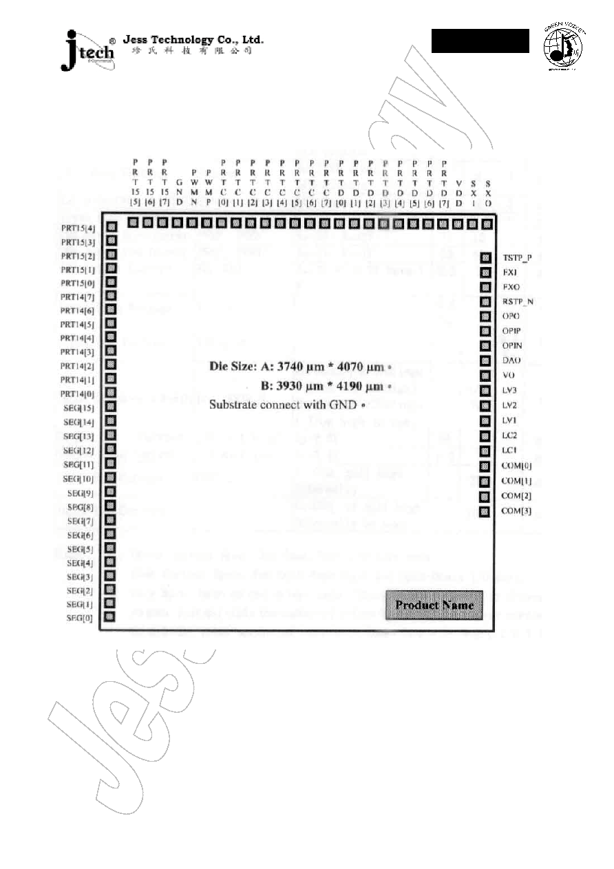
F. Pin Diagram
Suites 2202-7, Tower 6, The Gateway,
9 Canton Road, Tsimshatsui,
Kowloon, Hong Kong
Tel: (852) 2123 3289 Fax: (852) 2123 3393
E-mail: sales@jesstech.com
Home Page: www.jesstech.com
HE83715
HE80000 SERIES
03 MAY 2002
5 of 11
V 3.1
G. Bonding Pad Location
Version A:
PIN
Number
PIN
Name
X
Coordinate
Y
Coordinate
PIN
Number
PIN
Name
X
Coordinate
Y
Coordinate
1
SEG[8]
-1833.10
-932.70
37
PRTD[1]
422.15
1840.70
2
SEG[7]
-1833.10
-1067.85
38
PRTD[0]
296.50
1840.70
3
SEG[6]
-1833.10
-1203.00
39
PRTC[7]
170.90
1840.70
4
SEG[5]
-1833.10
-1338.15
40
PRTC[6]
45.30
1840.70
5
SEG[4]
-1833.10
-1473.35
41
PRTC[5]
-80.30
1840.70
6
SEG[3]
-1833.10
-1608.50
42
PRTC[4]
-205.90
1840.70
7
SEG[2]
-1833.10
-1743.65
43
PRTC[3]
-331.55
1840.70
8
SEG[1]
-1833.10
-1878.80
44
PRTC[2]
-457.15
1840.70
9
SEG[0]
-1833.10
-2013.95
45
PRTC[1]
-582.75
1840.70
10
COM[3]
1755.20
-721.65
46
PRTC[0]
-708.35
1840.70
11
COM[2]
1755.20
-587.60
47
PWMP
-859.75
1851.50
12
COM[1]
1755.20
-453.55
48
PWMN
-1034.80
1851.50
13
COM[0]
1755.20
-319.45
49
GND
-1184.00
1840.70
14
LC1
1755.20
-185.40
50
PRT15[7]
-1309.60
1840.70
15
LC2
1755.20
-51.30
51
PRT15[6]
-1435.20
1840.70
16
LV1
1755.20
82.75
52
PRT15[5]
-1560.80
1840.70
17
LV2
1755.20
316.80
53
PRT15[4]
-1833.10
1770.50
18
LV3
1755.20
350.90
54
PRT15[3]
-1833.10
1635.35
19
VO
1757.40
484.95
55
PRT15[2]
-1833.10
1500.20
20
DAO
1757.40
619.05
56
PRT15[1]
-1833.10
1365.05
21
OPIN
1755.20
753.10
57
PRT15[0]
-1833.10
1229.85
22
OPIP
1755.20
887.15
58
PRT14[7]
-1833.10
1094.70
23
OPO
1755.20
1021.25
59
PRT14[6]
-1833.10
959.55
24
RSTP_N
1755.20
1155.30
60
PRT14[5]
-1833.10
824.40
25
FXO
1755.20
1289.40
61
PRT14[4]
-1833.10
689.25
26
FXI
1755.20
1423.45
62
PRT14[3]
-1833.10
554.05
27
TSTP_P
1755.20
1557.50
63
PRT14[2]
-1833.10
418.90
28
SXO
1552.60
1840.70
64
PRT14[1]
-1833.10
283.75
29
SXI
1427.00
1840.70
65
PRT14[0]
-1833.10
148.60
30
VDD
1301.40
1840.70
66
SEG[15]
-1833.10
13.45
31
PRTD[7]
1175.80
1840.70
67
SEG[14]
-1833.10
-121.75
32
PRTD[6]
1050.20
1840.70
68
SEG[13]
-1833.10
-256.90
33
PRTD[5]
924.55
1840.70
69
SEG[12]
-1833.10
-392.05
34
PRTD[4]
798.95
1840.70
70
SEG[11]
-1833.10
-527.20
35
PRTD[3]
673.35
1840.70
71
SEG[10]
-1833.10
--662.35
36
PRTD[2]
547.75
1840.70
72
SEG[9]
-1833.10
-797.55