 | –≠–ª–µ–∫—Ç—Ä–æ–Ω–Ω—ã–π –∫–æ–º–ø–æ–Ω–µ–Ω—Ç: HE83750S | –°–∫–∞—á–∞—Ç—å:  PDF PDF  ZIP ZIP |

Suites 2202-7, Tower 6, The Gateway,
9 Canton Road, Tsimshatsui,
Kowloon, Hong Kong
Tel: (852) 2123 3289 Fax: (852) 2123 3393
E-mail: sales@jesstech.com
Home Page: www.jesstech.com
HE83750S
HE80000 SERIES
15 MAY 2002
1 of 11
V 2.1
A.HE83750S Introduction
HE83750S is a member of Jess Tech HE8000 series 8-bit CMOS micro-controller. This IC can
share the LCD pin and I/O pin (From 2048-dot of LCD driver + 16 Bit I/O Port ... 1792-dot of
LCD driver + 24 Bit I/O Port), the combination of the above is selected by Mask Option. It built-
in one internal Op-Amp, application to light, Sound, Temperature and Humidity sensor for
controlling application, one 7-bit D/A converter. Use the built-in 512KByte ROM can store
around large volume of data including voice, graphics and data. One DTMF generator. Suitable
in education toys, data-bank, translator and some mid-to-high end electronic products, Internal
SRAM recording, External SRAM or Flash RAM.
The HE83750S provides a very simple and effective instruction set, each instruction byte
occupies only 1.5 clock cycle time, therefore, it is suitable to apply in the high performance
systems.
B.HE83750S Features
!
Operating Voltage:
2.4V ≠3.6V
!
Operation frequency Range:
DC ~ 8MHz @ 3.6V
DC ~ 4MHz @ 2.4V
!
ROM size:
512K Bytes (64K Program Rom +448K Data Rom)
!
RAM size:
16K Bytes
!
Dual Clock:
Normal(Fast) clock:
32.768K ~ 8MHz
Slow
clock:
32.768KHz
!
Operating Mode:
DUAL FASTSLOWIDLESLEEP
!
Built-in WATCH DOG TIMER
!
16~24 bi-directional I/O pins, PUSH-PULL or OPEN DRAIN output selected by mask option
!
Built-in an internal Op-Amp
!
2048~1792 LCD driver. Built-in voltage booster circuitry to step up voltage supply for LCD,
but the maximum voltage after boosting should be less than 8.5 V.
!
Built-in DTMF generator
!
Built-in one 7-bit D/A Converter
!
Built-in a PWM output circuit
!
Provides three internal and two external interrupt
!
Provides two 16-bit timer, one time base timer
!
Instruction Set : 32 Instructions, 4 types of Addressing Mode, 2 individual Pointer for ROM
(19-bit) and RAM (14-bit) table access.
C.HE83750S Application
!
Interface to Light, Sound, Temperature and Humidity sensor for controlling application.
!
Suitable in LCD games, education toys, data-bank, translator and some mid-to-high end
electronic products.
Suites 2202-7, Tower 6, The Gateway,
9 Canton Road, Tsimshatsui,
Kowloon, Hong Kong
Tel: (852) 2123 3289 Fax: (852) 2123 3393
E-mail: sales@jesstech.com
Home Page: www.jesstech.com
HE83750S
HE80000 SERIES
15 MAY 2002
2 of 11
V 2.1
D. Pin Assignment
Pin
Pin Name
I/O
Function
Description
136
135
FXI,
FXO
B,
O
External Fast Clock pin.
Connecting to crystal or RC
to generate 32.768KHz ~
8MHz frequency.
139
138
SXI,
SXO
I,
O
External Slow Clock pin .
Connecting with 32768Hz
crystal or resistor as slow
clock and providing clock
source for LCD display,
TIMER1 and other internal
block.
Mask Option settings :
MO_FCK/SCKN=00Slow Clock only
01Illegal
10Dual Clock
11Fast Clock only
MO_FOSCE=0Internal fast oscillation
1External fast oscillation
MO_FXTAL=0RC oscillation for Fast Clock
1Crystal oscillation for Fast Clock
MO_SXTAL=0RC oscillation for 32.768K Clock
1X'tal oscillation for 32.768K Clock
Program the value of OP1and OP2 to change the operating
modes (Normal, Slow, Idle and Sleep). In Dual Clock
modethe main system clock is still the Fast Clock. The
32768Hz clock is for LCD and Timer1 only.
134
RSTP_N
I
System reset
Level trigger, active low. Except for using this pin, using
mask option (MO_PORE=1) could enable IC build-in
Power-on reset circuit.
Besides, MO_WDTE can set Watch Dog Timer
MO_WDTE =0Disable Watch Dog Timer
=1Enable Watch Dog Timer
137
TSTP_P
I
Test Pin.
Please bond this pin and add a test point on PCB for
debugging. Leave this pin floating is OK.
5..12
PRTC[7:0]
B
8-pin bi-directional I/O port
Mask Option
MO_CPP[7:0] =1 : Push-pull output
= 0 : Open-drain output.
Output must be "1" before reading whenever use the as
input (No tri-state structure).
145..
148
1..4
PRTD[7:0]
B
8-pin bi-directional I/O port.
PRTD[7:2] as wake-up pin.
PRTD[7:6] as external
interrupt pin.
Mask Option
MO_DPP[7:0] =1 : Push-pull output
= 0 : Open-drain output.
Output must be "1" before reading whenever use the as
input (No tri-state structure).
32..
39
PRT14[7:0]/
SEG[63:56]
B/
O
Port 14 bi-directional I/O
pin, (8 pins), or it can be
shared to LCD segment
Segment[63:56]
Mask Option
MO_LIO14[7:0] =1 LCD segment pin
=0 I/O pin,
MO_14PP[7:0]=1 : Push-pull output,
0 : Open-drain output
Output must be "1" before reading whenever use the as
input (No tri-state structure).
31..16
96..111 COM[15:0]
O
LCD COMmon Output
40...95 SEG[55:0]
O
LCD SEGment Output
LCD Data filled from 80H, please refer the LCD RAM
map.
112
L VL1
P
LCD Bias Voltage 1
113
L VL2
P
LCD Bias Voltage 2
114
L VL3
P
LCD Bias Voltage 3
115
L VL4
P
LCD Bias Voltage 4
116
L VL5
P
LCD Bias Voltage 5
LVP>LV5>LV4>LV3>LV2>LV1
LVP-0.5>=LV5 (be sure to keep 0.5 volt between LVP and
LV5 at lease.)
Adjust Resistor (R2) between LGS2 and LV5 to set LV5 for
LCD glass. The formula is LV5 = (1+R2/80K)*0.9V

Suites 2202-7, Tower 6, The Gateway,
9 Canton Road, Tsimshatsui,
Kowloon, Hong Kong
Tel: (852) 2123 3289 Fax: (852) 2123 3393
E-mail: sales@jesstech.com
Home Page: www.jesstech.com
HE83750S
HE80000 SERIES
15 MAY 2002
3 of 11
V 2.1
126
LGS1
I
Regulator Voltage Setting
Could adjust LVREG voltage
117
LGS2
I
LCD Drive Voltage Setting For LV5 voltage setting
118
L VP
P
Charge Pump Output
LVP=3(,4,5)*LVREG which setting by external capacitor
set LVP must small than 8.5Volt
119
LCAP4A
O
Charge Pump capacitor Pin
120
LCAP2B
O
Charge Pump capacitor Pin
121
LCAP2A
O
Charge Pump capacitor Pin
122
LCAP1A
O
Charge Pump capacitor Pin
123
LCAP1B
O
Charge Pump capacitor Pin
124
LCAP3A
O
Charge Pump capacitor Pin
Different capacitor Configuration make
LVP=3(,4,5)*LVREG.
The LCD driving circuit here makes regulation first, then
charge pump to LVP. IT generates bias voltage based on
LVP.
125
L VREG
O
Voltage Regulator Output
(To charge Pump Input)
Adjust to ~2.0 Volt by Resistor between LGS1 and LVREG
127
L VAG
O
Reference voltage Output
Fixed 0.9 Volt DC
13
PWMP
O
PWM positive output can
drive speaker or buzzer
directly.
Set the Bit2 of VOC register as one to turn on PWM.
14
PWMN
O
PWM negative output can
drive speaker or buzzer
directly.
Set the Bit2 of VOC register as one to turn on PWM.
129
VO
O
D/A voice output
Preset the Bit-1 of VOC register: DA=1turn on VO
130
DAO
O
D/A Output, for OP-Amp
use
Preset the Bit-1 of VOC register: OP=1turn on DAO
131
OPIN
I
OPAMP negative input pin
132
OPIP
I
OPAMP positive input pin
133
OPO
O
OPAMP output pin
Set the bit0(OP=1) of VOC register to turn on OP
comparator
142
DTMFO
O
DTMF Output
Turn on/off DTMF & write data via the port12
Use Mask Option MO_DTMFSCK to preset the clock
source:
MO_DTMFSCK=0Clock Source=3.579545 MHz
=1Clock Source=32768 Hz
141
MUTE
O
MUTE Output for Dialer
Turn on/off MUTE via the port12.
143
SDO
O
SDO for Dialer Application Turn on/off SDO & write data via the port12.
144
KEYTONE
O
1024 Hz 50% Duty Square
wave
Turn on/off KEYTONE via the port12.
140
VDD
P
Positive Power Input
128
GND
P
Power Ground Input
Adding 0.1
µ
F capacitor as by-pass capacitor is between
VDD and GND is necessary
15
VDD_RAM
P
Dedicated Power for RAM
E. LCD RAM Map
Page
1
SEG
[7:0]
SEG
[15:8]
SEG
[23:16]
SEG
[31:24]
SEG
[39:32]
SEG
[47:40]
SEG
[55:48]
SEG
[63:56]
COM0
00H
20H
40H
60H
80H
A0H
C0H
E0H
COM1
01H
21H
41H
61H
81H
A1H
C1H
E1H
COM2
02H
22H
42H
62H
82H
A2H
C2H
E2H
:
:
:
:
:
:
:
:
:
:
:
:
:
:
:
:
:
:
COM29
1DH
3DH
5DH
7DH
9DH
BDH
DDH
FDH
COM32
1EH
3EH
5EH
7EH
9EH
BEH
DEH
FEH
COM31
1FH
3FH
5FH
7FH
9FH
BFH
DFH
FFH
Suites 2202-7, Tower 6, The Gateway,
9 Canton Road, Tsimshatsui,
Kowloon, Hong Kong
Tel: (852) 2123 3289 Fax: (852) 2123 3393
E-mail: sales@jesstech.com
Home Page: www.jesstech.com
HE83750S
HE80000 SERIES
15 MAY 2002
4 of 11
V 2.1
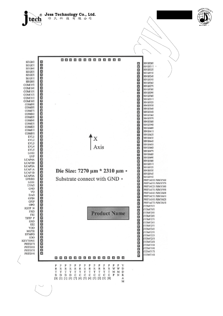
F. Bonding Diagram
Suites 2202-7, Tower 6, The Gateway,
9 Canton Road, Tsimshatsui,
Kowloon, Hong Kong
Tel: (852) 2123 3289 Fax: (852) 2123 3393
E-mail: sales@jesstech.com
Home Page: www.jesstech.com
HE83750S
HE80000 SERIES
15 MAY 2002
5 of 11
V 2.1
G. Pad Location
PIN
Number
PIN
Name
X
Coordinate
Y
Coordinate
PIN
Number
PIN
Name
X
Coordinate
Y
Coordinate
1
PRTD[3]
-3570.00
863.55
75
SEG[20]
3384.95
-1090.00
2
PRTD[2]
-3570.00
747.65
6
SEG[19]
3570.00
-696.95
3
PRTD[1]
-3570.00
631.72
77
SEG[18]
3570.00
-581.05
4
PRTD[0]
-3570.00
515.85
78
SEG[17]
3570.00
-465.15
5
PRTC[7]
-3570.00
399.95
79
SEG[16]
3570.00
-349.25
6
PRTC[6]
-3570.00
284.05
80
SEG[15]
3570.00
-233.35
7
PRTC[5]
-3570.00
168.15
81
SEG[14]
3570.00
-117.45
8
PRTC[4]
-3570.00
52.25
82
SEG[13]
3570.00
-1.55
9
PRTC[3]
-3570.00
-63.65
83
SEG[12]
3570.00
114.35
10
PRTC[2]
-3570.00
-179.55
84
SEG[11]
3570.00
230.20
11
PRTC[1]
-3570.00
-295.45
85
SEG[10]
3570.00
346.15
12
PRTC[0]
-3570.00
-411.35
86
SEG[9]
3570.00
462.05
13
PWMP
-3570.00
-528.55
87
SEG[8]
3570.00
577.95
14
PWMN
-3570.00
-644.45
88
SEG[7]
3570.00
693.85
15
VDD_RAM
-3570.00
-760.35
89
SEG[6]
3435.15
1090.00
16
COM[16]
-3556.60
-1090.00
90
SEG[5]
3319.25
1090.00
17
COM[17]
-3440.70
-1090.00
91
SEG[4]
3203.35
1090.00
18
COM[18]
-3324.80
-1090.00
92
SEG[3]
3087.45
1090.00
19
COM[19]
-3208.90
-1090.00
93
SEG[2]
2971.55
1090.00
20
COM[20]
-3093.00
-1090.00
94
SEG[1]
2855.65
1090.00
21
COM[21]
-2977.10
-1090.00
95
SEG[0]
2739.75
1090.00
22
COM[22]
-2861.20
-1090.00
96
COM[15]
2623.85
1090.00
23
COM[23]
-2745.30
-1090.00
97
COM[14]
2507.95
1090.00
24
COM[24]
-2629.40
-1090.00
98
COM[13]
2392.05
1090.00
25
COM[25]
-2513.50
-1090.00
99
COM[12]
2276.15
1090.00
26
COM[26]
-2397.60
-1090.00
100
COM[11]
2160.25
1090.00
27
COM[27]
-2281.70
-1090.00
101
COM[10]
2044.35
1090.00
28
COM[28]
-2165.80
-1090.00
102
COM[9]
1928.45
1090.00
29
COM[29]
-2049.90
-1090.00
103
COM[8]
1812.55
1090.00
30
COM[30]
-1934.00
-1090.00
104
COM[7]
1696.65
1090.00
31
COM[31]
-1818.10
-1090.00
105
COM[6]
1580.75
1090.00
32
PRT14[7]
-1702.20
-1090.00
106
COM[5]
1464.85
1090.00
33
PRT14[6]
-1586.30
-1090.00
107
COM[4]
1348.95
1090.00
34
PRT14[5]
-1470.40
-1090.00
108
COM[3]
1233.05
1090.00
35
PRT14[4]
-1354.50
-1090.00
109
COM[2]
1117.15
1090.00
36
PRT14[3]
-1238.60
-1090.00
110
COM[1]
1001.25
1090.00
37
PRT14[2]
-1122.70
1090.00
111
COM[0]
885.35
1090.00
38
PRT14[1]
-1006.80
1090.00
112
LVL1
769.45
1090.00
39
PRT14[0]
-890.90
1090.00
113
LVL2
653.55
1090.00
40
SEG[55]
-671.55
1090.00
114
LVL3
537.65
1090.00
41
SEG[54]
-555.65
1090.00
115
LVL4
421.75
1090.00
42
SEG[53]
-439.75
1090.00
116
LVL5
305.85
1090.00
43
SEG[52]
-323.85
1090.00
117
LGS2
189.95
1090.00
44
SEG[51]
-207.95
1090.00
118
LVP
74.05
1090.00
45
SEG[50]
-92.05
1090.00
119
LCAP4A
-41.85
1090.00