 | –≠–ª–µ–∫—Ç—Ä–æ–Ω–Ω—ã–π –∫–æ–º–ø–æ–Ω–µ–Ω—Ç: HE83R1402 | –°–∫–∞—á–∞—Ç—å:  PDF PDF  ZIP ZIP |
Suites 2202-7, Tower 6, The Gateway,
9 Canton Road, Tsimshatsui,
Kowloon, Hong Kong
Tel: (852) 2123 3289 Fax: (852) 2123 3393
E-mail: sales@jesstech.com
Home Page: www.jesstech.com
HE83R140
HE80000 SERIES
01 APR 2002
1 of 10
PreliminaryV1.02
A.HE83R1402 Introduction
HE83R1402
is a member of 8-bit Micro-controller series developed by JESS
.
Users can chose any
one of combination among 1024 dots LCD Driver + 16 Bit I/O Port...896 dots LCD Driver +
24 Bit I/O Portetc. The built-in OP comparator can be used with (lightvoicetemperature
humility) sensor and used as battery low detection. The 7-bit current-type D/A converter and PWM
device provide the complete speech output mechanism. The 320K ROM Size can be used in the
storage of speechgraphictext etc.. . It can be applicable to the medium systems such as Small-
Scale Dictionary, Data Bank, Educational Toy, Digital Voice Recording System etc. It also can be
connected to SRAM or Flash RAM for recording function.
The instruction set of HE83R1402 are quite easy to learn and simple to use. Only about thirty
instructions with four-type addressing mode are provided. Most of instructions take only 3
oscillator clocks (machine cycles). The processing power is enough to most of battery operation
system.
B.HE83R1402 Features
Operation Voltage
2.4V ≠ 5.2V
System Clock
DC ~ 8MHz @ 5.0V
DC ~ 4MHz @ 2.4V
Internal ROM
320K Bytes
Internal RAM
1K Bytes
Dual Clock System
Normal (Fast) clock 32.768K ~ 8MHz
Slow
clock 32.768KHz
Operation Mode
DUALFASTSLOWIDLESLEEP Mode.
With WDT (WATCH DOG TIMER) to prevent deadlock condition.
16~24 bit Bi-directional I/O port.
Mask Option can select PUSH-PULL or OPEN DRAIN
output mode for each I/O pin. 8 of them are shared with LCD segment pins.
One built-in OP comparator.
1024~896 dots LCD driver (B TYPE selectable).
(No LCD contrast control function)
Build in LCD Voltage Regulator.
One 7-bit current-type DAC output.
PWM device.
Two external interrupts and three internal timer interrupts.
Two 16-bit timers and one Time-Base timer.
Instruction set 32 instructions, 4 addressing mode. 10-bit DATA POINTER for RAM and
19-bit TABLE POINTER for ROM.

Suites 2202-7, Tower 6, The Gateway,
9 Canton Road, Tsimshatsui,
Kowloon, Hong Kong
Tel: (852) 2123 3289 Fax: (852) 2123 3393
E-mail: sales@jesstech.com
Home Page: www.jesstech.com
HE83R140
HE80000 SERIES
01 APR 2002
2 of 10
PreliminaryV1.02
C. Internal Block
Small-Scale Dictionary, Data Bank, Educational Toy, Digital Voice Recording System etc.
D. Pin Description
Pin#
Pin name I/O
Function
Description
111,
110
FXI,
FXO
B,
O
External fast clock pin.
Connecting to crystal or RC
to generate 32.768 kHz ~
8MHz frequency.
114,
113
SXI,
SXO
I,
O
External slow clock pin.
Connecting with 32768 Hz
crystal or resistor as slow
clock and providing clock
source for LCD display,
TIMER1, Time-Base and
other internal blocks.
Mask option setting
MO_FCK/SCKN = 00Slow Clock only
01Illegal
10Dual Clock
11Fast Clock only
MO_FOSCE = 0Internal fast osc.
= 1External fast osc.
MO_FXTAL = 0RC osc. for fast clock
= 1X'tal osc. for fast clock
MO_SXTAL = 0RC for 32768 Hz clock
= 1X'tal for 32768 Hz clock
Use OP1 and OP2 to switch among different operation
mode (NORMAL, SLOW, IDEL and SLEEP). In Dual
Clock mode, the main system clock is still the Fast
Clock. The 32768 Hz clock is for LCD and Timer 1 only.
109
RSTP_N
I System Reset.
Level trigger, active low. Except for using this pin, using
mask option (MO_PORE=1) could enable IC build-in
Power-on reset circuit.
Besides, MO_WDTE can set Watch Dog Timer
MO_WDTE=0Disable Watch Dog Timer
=1Enable Watch Dog Timer
112
TSTP_P
I Test Pin
Please bond this pin and add a test point on PCB for
debugging. But for improving ESD, please connect
this pin with zero Ohm resistor to GND.
124..127,
1..4
PRTC[7:0] B 8-pin bi-directional I/O port.
Mask options
MO_CPP[7..0]=1 ~ Push-pull.
=0 ~ Open-drain.
Output must be "1" before reading whenever use them as
input (No tri-state structure).
116..
123
PRTD[7:0] B
8-pin bi-directional I/O port.
PRTD[7..2] as wake-up pin.
PRTD[7..6] as external
interrupt pin.
Mask options
MO_DPP[7..0]=1 ~ Push-pull.
=0 ~ Open-drain.
Output must be "1" before reading whenever use them as
input (No tri-state structure).
15..22 PRT14[7:0]/
SEG[63:56]
B/
O
8-pin bi-directional I/O port
that is shared with LCD
segment pin.
Mask options
MO_LIO14[7..0]=1 ~ LCD Pin.
=0 ~ I/O Pin.
MO_14PP[7..0]=1 ~ Push-pull.
=0 ~ Open-drain.
Output must be "1" before reading whenever use them as
input (No tri-state structure).
Suites 2202-7, Tower 6, The Gateway,
9 Canton Road, Tsimshatsui,
Kowloon, Hong Kong
Tel: (852) 2123 3289 Fax: (852) 2123 3393
E-mail: sales@jesstech.com
Home Page: www.jesstech.com
HE83R140
HE80000 SERIES
01 APR 2002
3 of 10
PreliminaryV1.02
Pin#
Pin name I/O
Function
Description
14..7
79..86
COM[15:0] O LCD COMmon Output
23..
78
SEG[55:0]
O LCD SEGment Output
LCD Data filled from F0H, please refer the LCD RAM
map.
101
L V1
B LCD Bias Voltage 1
100
L V2
B LCD Bias Voltage 2
89
L V3
B LCD Bias Voltage 3
88
L V4
B LCD Bias Voltage 4
87
L V5
B LCD Bias Voltage 5
LV5> LV4> LV3> LV2> LV1
Adjust Resistor between LCDGS and LV2 to set LV5 for
LCD glass. The formula is LV5 = 2.5*LV2(Bias=1/5)
Suggest that LV2=2.0V, so LV5=5.0V.
99
LCDGS
B LCD Gain Setting Pin
~300K between LCDGS and LV2 LV2
2.0 Volt
90
LCDVTB
B Charge Pump Capacitor Pin Larger voltage stair than LCxA, LCxB stair
102
LCDVX
B Charge Pump Capacitor Pin Smaller voltage stair than LCxA, LCxB stair
91
LC4B
B Charge Pump Capacitor Pin
92
LC4A
B Charge Pump Capacitor Pin
93
LC3B
B Charge Pump Capacitor Pin
94
LC3A
B Charge Pump Capacitor Pin
95
LC2B
B Charge Pump Capacitor Pin
96
LC2A
B Charge Pump Capacitor Pin
97
LC1B
B Charge Pump Capacitor Pin
98
LC1A
B Charge Pump Capacitor Pin
Different LCD Bias must be matching its
Capacitor
Configuration
relatively. This IC is with all pins for type-
IV LCD Driver. Some of charge pump pins was not using
since the bias of this IC was fixed at 1/5.
5
PWM
O
The PWM output can drive
speaker or buzzer directly.
Set the bit2 of VOC register as one to turn on PWM.
104
VO
O D/A output.
Bit 1 of VOC = `1' , Turn on DA
105
DAO
O DAC Voice Output
Set the bit1(DA=1) of VOC register to turn on DAC with
VO output.
106
OPIN
I OPAMP negative input pin.
107
OPIP
I OPAMP positive input pin.
108
OPO
O OPAMP output pin.
Built-in OP comparator.
Set Bit 0 of VOC = `1' , Turn on OP
115
VDD
P Positive Power Input
103
GND
P Power Ground Input
6
GND_PWM P Dedicated PWM Ground
Adding 0.1 µF capacitor as by-pass capacitor on power
pins is necessary.(within 1 cm distance)
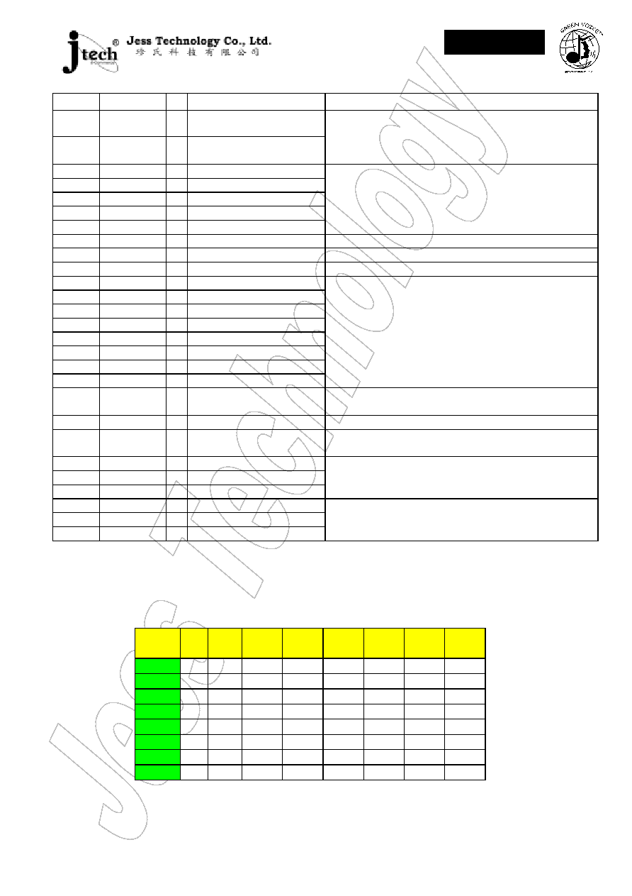
E.LCD RAM Map
Page
0
SEG
[7:0]
SEG
[15:8]
SEG
[23:16]
SEG
[31:24]
SEG
[39:32]
SEG
[47:40]
SEG
[55:48]
SEG
[63:56]
COM0 80H 90H A0H
B0H
C0H
D0H
E0H
F0H
COM1 81H 91H A1H
B1H
C1H
D1H
E1H
F1H
COM2 82H 92H A2H
B2H
C2H
D2H
E2H
F2H
:
:
:
:
:
:
:
:
:
:
:
:
:
:
:
:
:
:
COM13 8DH 9DH ADH BDH CDH DDH EDH
FDH
COM14 8EH 9EH AEH
BEH
CEH
DEH
EEH
FEH
COM15 8FH 9FH AFH
BFH
CFH
DFH
EFH
FFH

Suites 2202-7, Tower 6, The Gateway,
9 Canton Road, Tsimshatsui,
Kowloon, Hong Kong
Tel: (852) 2123 3289 Fax: (852) 2123 3393
E-mail: sales@jesstech.com
Home Page: www.jesstech.com
HE83R140
HE80000 SERIES
01 APR 2002
4 of 10
PreliminaryV1.02
F. Pin Diagram
Die Size: 4520 µm * 3910 µm
Substrate connect with GND
Product Name
P
R
T
C
[
4
]
P
R
T
C
[
5
]
P
R
T
C
[
6
]
P
R
T
C
[
7
]
P
R
T
D
[
0
]
P
R
T
D
[
1
]
P
R
T
D
[
2
]
P
R
T
D
[
3
]
P
R
T
D
[
4
]
P
R
T
D
[
5
]
P
R
T
D
[
6
]
P
R
T
D
[
7
]
V
D
D
S
X
I
S
X
O
T
S
T
P
_
P
F
X
I
F
X
O
R
S
T
P
_
N
O
P
O
O
P
I
P
O
P
I
N
D
A
O
V
O
G
N
D
L
C
D
V
X
L
V
1
L
V
2
L
C
D
G
S
L
C
1
A
L
C
1
B
L
C
2
A
L
C
2
B
S
E
G
[4
6]
S
E
G
[4
5]
S
E
G
[4
4]
S
E
G
[4
3]
S
E
G
[4
2]
S
E
G
[4
1]
S
E
G
[4
0]
S
E
G
[3
9]
S
E
G
[3
8]
S
E
G
[3
7]
S
E
G
[3
6]
S
E
G
[3
5]
S
E
G
[3
4]
S
E
G
[3
3]
S
E
G
[3
2]
S
E
G
[3
1]
S
E
G
[3
0]
S
E
G
[2
9]
S
E
G
[2
8]
S
E
G
[2
7]
S
E
G
[2
6]
S
E
G
[2
5]
S
E
G
[2
4]
S
E
G
[2
3]
S
E
G
[2
2]
S
E
G
[2
1]
S
E
G
[2
0]
S
E
G
[1
9]
S
E
G
[1
8]
S
E
G
[1
7]
S
E
G
[1
6]
S
E
G
[1
5]
PRTC[3]
PRTC[2]
PRTC[1]
PRTC[0]
PWM
GND_PWM
COM[8]
COM[9]
COM[10]
COM[11]
COM[12]
COM[13]
COM[14]
COM[15]
PRT14[7]/SEG[63]
PRT14[6]/SEG[62]
PRT14[5]/SEG[61]
PRT14[4]/SEG[60]
PRT14[3]/SEG[59]
PRT14[2]/SEG[58]
PRT14[1]/SEG[57]
PRT14[0]/SEG[56]
SEG[55]
SEG[54]
SEG[53]
SEG[52]
SEG[51]
SEG[50]
SEG[49]
SEG[48]
SEG[47]
LC3A
LC3B
LC4A
LC4B
LCDVTB
LV3
LV4
LV5
COM[0]
COM[1]
COM[2]
COM[3]
COM[4]
COM[5]
COM[6]
COM[7]
SEG[0]
SEG[1]
SEG[2]
SEG[3]
SEG[4]
SEG[5]
SEG[6]
SEG[7]
SEG[8]
SEG[9]
SEG[10]
SEG[11]
SEG[12]
SEG[13]
SEG[14]
Suites 2202-7, Tower 6, The Gateway,
9 Canton Road, Tsimshatsui,
Kowloon, Hong Kong
Tel: (852) 2123 3289 Fax: (852) 2123 3393
E-mail: sales@jesstech.com
Home Page: www.jesstech.com
HE83R140
HE80000 SERIES
01 APR 2002
5 of 10
PreliminaryV1.02
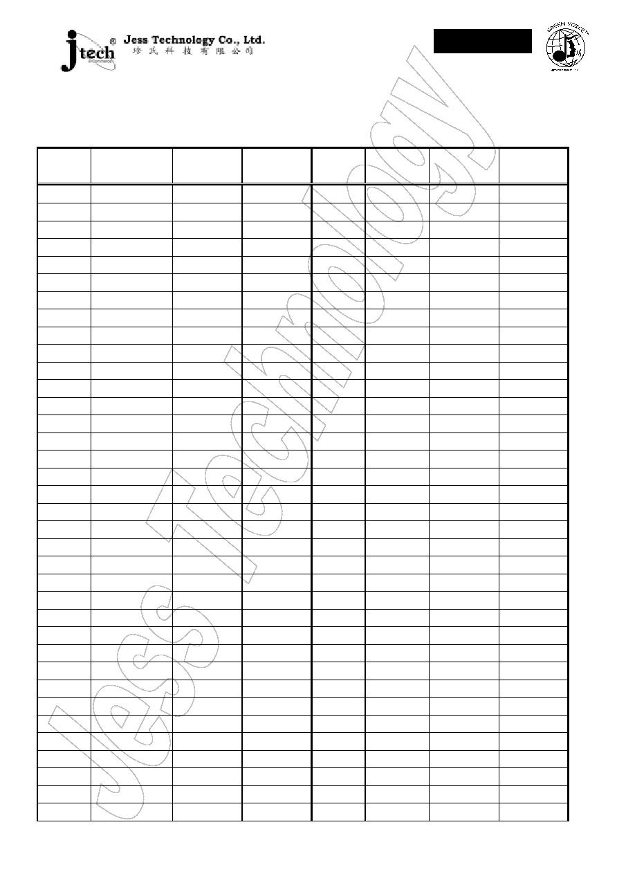
G. Bonding Pad Location
PIN
Number
PIN
Name
X
Coordinate
Y
Coordinate
PIN
Number
PIN
Name
X
Coordinate
Y
Coordinate
1
PRTC[3]
-2190.00
1839.70
65
SEG[13]
2190.00
-1597.80
2
PRTC[2]
-2190.00
1724.70
66
SEG[12]
2190.00
-1482.80
3
PRTC[1]
-2190.00
1609.70
67
SEG[11]
2190.00
-1367.80
4
PRTC[0]
-2190.00
1494.70
68
SEG[10]
2190.00
-1252.80
5
PWM
-2190.00
1379.70
69
SEG[9]
2190.00
-1137.80
6
GND_PWM
-2190.00
1264.70
70
SEG[8]
2190.00
-1022.80
7
COM[8]
-2190.00
1131.40
71
SEG[7]
2190.00
-907.80
8
COM[9]
-2190.00
1016.90
72
SEG[6]
2190.00
-792.80
9
COM[10]
-2190.00
901.90
73
SEG[5]
2190.00
-593.60
10
COM[11]
-2190.00
786.90
74
SEG[4]
2190.00
-478.60
11
COM[12]
-2190.00
671.90
75
SEG[3]
2190.00
-363.60
12
COM[13]
-2190.00
556.90
76
SEG[2]
2190.00
-248.60
13
COM[14]
-2190.00
441.90
77
SEG[1]
2190.00
-133.60
14
COM[15]
-2190.00
326.90
78
SEG[0]
2190.00
-18.60
15
PRT14[7]
-2190.00
211.40
79
COM[7]
2190.00
96.40
16
PRT14[6]
-2190.00
96.40
80
COM[6]
2190.00
211.40
17
PRT14[5]
-2190.00
-18.60
81
COM[5]
2190.00
326.40
18
PRT14[4]
-2190.00
-133.60
82
COM[4]
2190.00
441.40
19
PRT14[3]
-2190.00
-248.60
83
COM[3]
2190.00
556.40
20
PRT14[2]
-2190.00
-363.60
84
COM[2]
2190.00
671.40
21
PRT14[1]
-2190.00
-478.60
85
COM[1]
2190.00
786.40
22
PRT14[0]
-2190.00
-593.60
86
COM[0]
2190.00
901.40
23
SEG[55]
-2190.00
-792.80
87
LV5
2190.00
1023.00
24
SEG[54]
-2190.00
-907.80
88
LV4
2190.00
1138.00
25
SEG[53]
-2190.00
-1022.80
89
LV3
2190.00
1253.00
26
SEG[52]
-2190.00
-1137.80
90
LCDVTB
2190.00
1368.00
27
SEG[51]
-2190.00
-1252.80
91
LC4B
2190.00
1483.00
28
SEG[50]
-2190.00
-1367.80
92
LC4A
2190.00
1598.00
29
SEG[49]
-2190.00
-1482.80
93
LC3B
2190.00
1713.00
30
SEG[48]
-2190.00
-1597.80
94
LC3A
2190.00
1828.00
31
SEG[47]
-2190.00
-1841.60
95
LC2B
1871.05
1885.00
32
SEG[46]
-1829.60
-1885.00
96
LC2A
1756.05
1885.00
33
SEG[45]
-1714.60
-1885.00
97
LC1B
1641.05
1885.00
34
SEG[44]
-1599.60
-1885.00
98
LC1A
1526.05
1885.00
35
SEG[43]
-1484.60
-1885.00
99
LCDGS
1411.05
1885.00
36
SEG[42]
-1369.60
-1885.00
100
LV2
1296.05
1885.00