
HE8P1602
Page 1
Version 1.5
HE8P1602 PRODUCT SPECIFICATION
1.
GENERAL DESCRIPTION .................................................................................................................................................... 3
2.
FEATURES ............................................................................................................................................................................... 3
3.
PIN ASSIGNMENT.................................................................................................................................................................. 3
4.
BLOCK DIAGRAM ................................................................................................................................................................. 4
5.
PIN DESCRIPTION ................................................................................................................................................................. 4
6.
PROGRAM MEMORY (ROM) .............................................................................................................................................. 5
7.
DATA MEMORY (RAM) ........................................................................................................................................................ 5
7.1
RAM BANK LOCATION ................................................................................................................................................ 5
7.2
SYSTEM REGISTER ARRANGEMENT (BANK 0)...................................................................................................... 6
8.
ACCUMULATOR .................................................................................................................................................................... 8
8.1
CARRY FLAG.................................................................................................................................................................. 8
8.2
DECIMAL CARRY FLAG............................................................................................................................................... 8
8.3
ZERO FLAG ..................................................................................................................................................................... 8
9.
WORKING REGISTERS ........................................................................................................................................................ 8
9.1
Y, Z REGISTERS ............................................................................................................................................................. 8
9.2
LOOK-UP TABLE............................................................................................................................................................ 9
9.3
ADDRESSING MODE ..................................................................................................................................................... 9
10.
PROGRAM COUNTER...................................................................................................................................................... 9
10.1
ONE ADDRESS SKIPPING........................................................................................................................................... 10
10.2
MULTI-ADDRESS JUMPING....................................................................................................................................... 10
11.
STACK BUFFER ............................................................................................................................................................... 10
11.1
ACC & WORKING REGISTERS PROTECTION ........................................................................................................ 11
12.
OSCILLATOR ................................................................................................................................................................... 11
12.1
OSCM REGISTER.......................................................................................................................................................... 11
12.2
O
SCILLATOR
O
PTION
........................................................................................................................................................ 12
12.3
INTERNAL LOW CLOCK ............................................................................................................................................ 12

HE8P1602
Page 2
Version 1.5
12.4
HIGH-LOW CLOCK EXCHANGE ............................................................................................................................... 12
12.5
0.5 SECOND RESTART
FUNCTION ........................................................................................................................... 13
13.
GTMR PRESCALER ........................................................................................................................................................ 13
13.1
WARMUP TIME ............................................................................................................................................................ 13
13.2
WATCH DOG (WDOG) TIMER ................................................................................................................................... 14
14.
TIMER/EVENT COUNTER (TC0) ................................................................................................................................. 15
14.1
TC0M MODE REGISTER.............................................................................................................................................. 15
14.2
TC0C COUNTING REGISTER ..................................................................................................................................... 15
15.
INTERRUPT ...................................................................................................................................................................... 16
15.1
INTEN INTERRUPT ENABLE REGISTER ................................................................................................................. 16
15.2
INTRQ INTERRUPT REQUEST REGISTER ............................................................................................................... 16
16.
I/O PORT............................................................................................................................................................................ 17
16.1
PORT MODE (P
N
M) REGISTER .................................................................................................................................. 17
16.2
PORT (P
N
) DATA REGISTER....................................................................................................................................... 18
16.3
PORT 1 WAKEUP (P1W) REGISTER .......................................................................................................................... 18
17.
APPLICATION NOTE...................................................................................................................................................... 19
18.
ABSOLUTE MAXIMUM RATING................................................................................................................................. 20
19.
ELECTRICAL CHARACTERISTIC.............................................................................................................................. 20
20.
INSTRUCTION SET ......................................................................................................................................................... 21
21.
PACKAGE INFORMATION :......................................................................................................................................... 22

HE8P1602
Page 3
Version 1.5
HE8P1602 8-bit micro-controller
1. GENERAL DESCRIPTION
he HE8P1602 is an 8-bit micro-controller utilized with CMOS technology fabrication and featured with low power
consumption and high performance by its unique electronic structure. This chip is designed with the excellent IC structure,
including the program memory up to 1024-word OTP ROM, 48 bytes of the data memory, one 8-bit timer/event counter, watch
dog timer, two interrupt sources (TC0, INT0), 14 I/O pins and 4 levels stack buffer. Besides, the user can choose desired oscillator
configurations for the controller. There are four external oscillator configurations to select for generating system clock, including
high-performing crystal, ceramic resonator, cost-saving RC and internal RC oscillator.
2. FEATURES
Memory configuration
Two interrupt sources :
OTP ROM size : 1024 * 16 bits.
One internal interrupts : TC0
RAM size : 48 * 8 bits.
One external interrupt : INT0
I/O pin configuration (Total 14 pins)
Four levels stack buffer
One input pin with interrupt function
Bi-direction Input/output ports : 13 pins
Five pins with wake-up function
An 8-bit timer/event counter.
A watchdog timer.
Built-in voltage detector to protect the Brown-out Reset
Acceptable oscillator type :
Crystal or ceramic resonator speed up to 20MHz
56 powerful instructions
RC oscillator type speed up to 10MHz
All of instructions are 1 word with 1 or 2 cycles'
execution.
Internal RC oscillator 16KHz
Execution time : 1 cycle uses 4 clocks of oscillator.
All ROM area JMP instruction.
Package :
All ROM area Subroutine CALL instruction.
PDIP : 18
All ROM area lookup table function. (MOVC instruction)
SOP : 18
SSOP : 20
3. PIN ASSIGNMENT
P1.2
1 U 20
P1.1
P1.2
1 U 18 P1.1
P1.3
2
19
P1.0
P1.3
2
17 P1.0
INT0/P0.0
3
18
XIN
INT0/P0.0
3
16 XIN
RST
4
17
XOUT/P1.4
RST
4
15 XOUT/P1.4
VSS
5
16
VDD
VSS
5
14 VDD
VSS
6
15
VDD
P2.0
6
13 P2.7
P2.0
7
14
P2.7
P2.1
7
12 P2.6
P2.1
8
13
P2.6
P2.2
8
11 P2.5
P2.2
9
12
P2.5
P2.3
9
10 P2.4
P2.3
10
11
P2.4
HE8P1602P
HE8P1602X
HE8P1602S
X:SSOP
T
HE8P1602
Page 4
Version 1.5
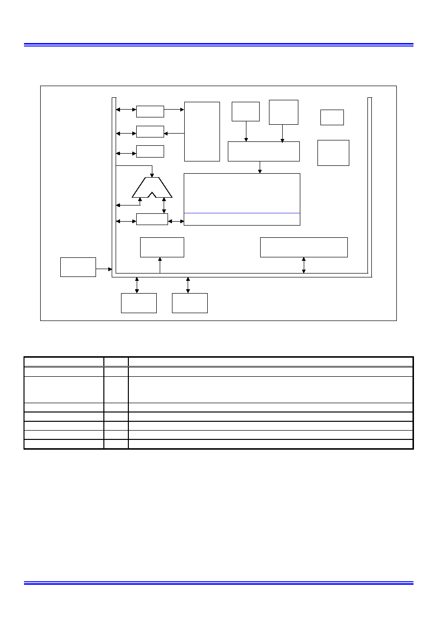
4. BLOCK DIAGRAM
PC
IR
ROM
H-OSC
TIMING GENERATOR
RAM
SYSTEM REGISTER
ALU
ACC
INTERRUPT
CONTROL
TIMER & COUNTER
PORT 0
PORT 2
PORT 1
FLAGS
Internal
RC
LVD
Watch
Dog
PC
IR
ROM
H-OSC
TIMING GENERATOR
RAM
SYSTEM REGISTER
ALU
ACC
INTERRUPT
CONTROL
TIMER & COUNTER
PORT 0
PORT 2
PORT 1
FLAGS
Internal
RC
LVD
Watch
Dog
5. PIN DESCRIPTION
PIN NAME
TYPE
DESCRIPTION
P1.0 ~ P1.4
I/O
Port 1.0 ~ Port 1.4 bi-direction pins with sleep mode wake-up function
RST/VPP
I
System reset inputs pin. Schmitt trigger structure, active "low", normal stay to "high".
During program op-code, this pin be pull to 12.5Vdc to reset internal address counter and to
write data into OTP-ROM.
VDD, VSS
P
Power supply input pins.
P2.0 ~ P2.7
I/O
Port 2.0 ~ Port 2.7 bi-direction pins.
XIN
I
Oscillator input pin.
XOUT/P1.4
I/O
Oscillator output pin. RC Mode as the P1.4 I/O
P0.0/INT0
I
Port 0.0 and INT0 trigger pin with Schmitt trigger structure or wake-up from sleep mode

HE8P1602
Page 5
Version 1.5
6. PROGRAM MEMORY (ROM)
The HE8P1602 provides the program memory up to 1024-word ( 1024 * 16 bits) to be addressed and is able to fetch instructions
through 10-bit wide PC (Program Counter). It also can lookup ROM data by using ROM code registers (Y, Z). All of the program
memory is partitioned into two coding areas, located from 000H to 00FH and from 010H to 3FFH. The former area is assigned for
executing interrupt vector. And the later area is for storing instruction's OP-code and lookup table's data. The last location (3FFH)
of OTP ROM had been reserved, it can not be used by programming.
OTP ROM
000h
Reset vector
001h
002h
003h
004h
Reserved
005h
"
006h
"
007h
"
008h
Interrupt vector
009h
.
00Ah
.
.
.
.
.
010h
General purpose area
.
.
.
.
.
.
.
.
.
.
.
.
3FEh
.
3FFh
Reserved
7. DATA MEMORY (RAM)
The HE8P1602 has built-in 48 bytes memory location to store general purpose data and built-in special purpose memory to work
as system registers. These memory locations are allocated in RAM bank 0, first 48-byte (00H ~ 2FH) shared for general data
memory and last 128 bytes (80H ~ FFH) shared for system registers.
7.1 RAM BANK LOCATION
RAM location
00h
General purpose area
2Fh
End of Ram
80h
System registers
"
"
"
"
FFh
"