 | –≠–ª–µ–∫—Ç—Ä–æ–Ω–Ω—ã–π –∫–æ–º–ø–æ–Ω–µ–Ω—Ç: HF88F04 | –°–∫–∞—á–∞—Ç—å:  PDF PDF  ZIP ZIP |
Suites 2202-7, Tower 6, The Gateway,
9 Canton Road, Tsimshatsui,
Kowloon, Hong Kong
Tel: (852) 2123 3289 Fax: (852) 2123 3393
E-mail: sales@jesstech.com
Home Page: www.jesstech.com
HF88F04
HE80000 SERIES
Command Mode Flash
-1-
02/04/29
Preliminary Target Specification
Product Name
Command Mode Flash Memory
JESS Doc. No.
HF88F04.doc
JESS Product. No.
HF88F04
≠ Table of Contents ≠
1.
General Description
____________________________________________________ 2
2.
Features
______________________________________________________________ 2
3.
Pin Description
________________________________________________________ 3
4.
Pad Diagram
__________________________________________________________ 4
5.
Pad Coordinates
_______________________________________________________ 4
6.
Function Block Diagram
________________________________________________ 5
7.
Parallel Mode
_________________________________________________________ 6
7.1.
Parallel Write Command Mode
_________________________________________ 6
7.2.
Parallel Write Data Mode
______________________________________________ 7
7.3.
Parallel Read Data Mode
______________________________________________ 7
7.4.
Parallel Read Checksum Mode
__________________________________________ 8
8.
Serial Mode
___________________________________________________________ 8
8.1.
Bi-directional Synchronous Serial Data Interface
__________________________ 9
8.2.
Serial Write Command Mode
___________________________________________ 9
8.3.
Serial Write Data Mode
_______________________________________________ 10
8.4.
Serial Read Data Mode
_______________________________________________ 10
8.5.
Serial Read Checksum Mode
__________________________________________ 11
9.
Power consideration
___________________________________________________ 11
10.
Absolute Maximum Rating
____________________________________________ 12
11.
AC Electrical Characteristics
__________________________________________ 12
12.
Electrical Characteristics
_____________________________________________ 12
13.
Application Circuit
__________________________________________________ 12

Suites 2202-7, Tower 6, The Gateway,
9 Canton Road, Tsimshatsui,
Kowloon, Hong Kong
Tel: (852) 2123 3289 Fax: (852) 2123 3393
E-mail: sales@jesstech.com
Home Page: www.jesstech.com
HF88F04
HE80000 SERIES
Command Mode Flash
-2-
02/04/29
1.
General Description
The HF88F04 is a command mode flash device. It features parallel and serial bi-directional dual
access modes. Multiple device array can be accessed with only minimal additional device select
pin. Simple exclusive or checksum provides error detection during data transfer between MCU
and the device. The interface logic and protocol include setting up the starting address for data
transfer, writing data into Flash Memory, as well as read it back for verification, and error checking
by Exclusive OR checksum. It can be used for non-volatile memory extension for all JESS's
MCUs.
Chip Select pins allows array of HF88F04 devices are used simultaneously for both parallel and
serial transfer mode. In the serial mode, the HF88F04 is connected in daisy chain configuration to
minimize the I/O pin required to use multi-chip array, while in parallel mode, the devices share
most of the control pins and data bus except the chip select pins.
2.
Features
!
Dual (parallel and serial) command access modes.
!
Address automatically increment with each Read/Write data access.
!
Page erase mode and erase verify mode.
!
Exclusive or checksum error detection
!
Multiple chip array is allowed with easy addressing logic
!
Read access voltage range 2.2V ~ 3.6V
!
Organization
-
Memory Cell Array: 512K x 8
!
Package ≠ Dice form

Suites 2202-7, Tower 6, The Gateway,
9 Canton Road, Tsimshatsui,
Kowloon, Hong Kong
Tel: (852) 2123 3289 Fax: (852) 2123 3393
E-mail: sales@jesstech.com
Home Page: www.jesstech.com
HF88F04
HE80000 SERIES
Command Mode Flash
-3-
02/04/29
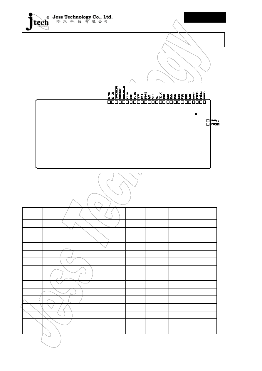
3.
Pin Description
HF88F04
15
13
12
20
5
17
18
14
9
8
7
6
1
4
16
19
3
10
2
11
D7
D5
D4
VDD
R_WN
SDI
SDO
D6
D3
D2
D1
D0
P_SN
D_CN
SCLK
CS1
CS0N
BUSY
VSS
NC
Symbol
Pin
No.
I/O Description
P_Sn
I
Input to select either parallel (when `1') or serial (when `0') interface is
used for transferring data.
VSS
I
Negative power supply of the device
CS0n
I
CS0n is active low chip select input pin. The device is selected when
CS1 is high and CS0n is low simultaneously. Otherwise, it is deselected.
D_Cn
I
Input to select either the FLASH memory or Registers (TPP, TPH, TPL,
Mode or Checksum).
R_Wn
I
Input to select either a Read operation (when `1') or a write operation
(when `0') is to be performed.
Busy
O
Busy indicator output. When high, it indicates the FLASH is occupied
in internal process.
D0 ~ D7
I/O Bi-directional data bus for parallel transfer mode.
SCLK/
Strobe
I
This pin is shared between parallel and serial modes. In serial mode,
this pin is serial clock SCLK for transferring the data from/to SDI/SDO.
In parallel mode, it is the strobe signal used to write the registers and
FLASH as well as read the checksum and contents of FLASH memory.
This pin is equipped with Schmidt type input structure to prevent the
input from chattering due to slow rising clock source transition.
SDI
I
Serial Data Input for writing to either Registers or Flash Memory.
SDO
O
Serial Data Output for reading data from either Checksum Register or
Flash Memory.
CS1
I
CS1 is active high chip select input. The device is selected when CS1 is
high and CS0n is low simultaneously. Otherwise, it is deselected.
VDD
I
Positive power supply of the device
Suites 2202-7, Tower 6, The Gateway,
9 Canton Road, Tsimshatsui,
Kowloon, Hong Kong
Tel: (852) 2123 3289 Fax: (852) 2123 3393
E-mail: sales@jesstech.com
Home Page: www.jesstech.com
HF88F04
HE80000 SERIES
Command Mode Flash
-4-
02/04/29
4.
Pad Diagram
5.
Pad Coordinates
Pin
Number
Pin
Name
X
Coordinate
Y
Coordinate
Pin
Number Name
X
Coordinate
Y
Coordinate
1
P_SN
340.5
1022.7
16
D[1]
1950.51
1022.7
2
GND
225.5
1022.7
17
D[2]
1835.51
1022.7
3
CS0N
110.5
1022.7
18
D[3]
1720.51
1022.7
4
STROBE[2]
-4.5
1022.7
19
D[4]
1605.51
1022.7
5
STROBE[1]
-119.5
1022.7
20
D[5]
1490.51
1022.7
6
STROBE[0]
-234.5
1022.7
21
D[6]
1375.51
1022.7
7
D_CN
-349.5
1022.7
22
D[7]
1260.51
1022.7
8
R_WN
-464.5
1022.7
23
SCLK
1145.51
1022.7
9
PMS[0]
2632.97
332.41
24
SDI
1030.51
1022.7
10
PMS[1]
2632.61
448.7
25
SDO
915.51
1022.7
11
PMS[2]
2525.51
1022.7
26
MX
800.5
1022.7
12
PMS[3]
2410.51
1022.7
27
PPWD
685.5
1022.7
13
PMS[4]
2295.51
1022.7
28
CS1
570.5
1022.7
14
BUSY
2180.51
1022.7
29
VDD
455.5
1022.7
15
D[0]
2065.51
1022.7
Suites 2202-7, Tower 6, The Gateway,
9 Canton Road, Tsimshatsui,
Kowloon, Hong Kong
Tel: (852) 2123 3289 Fax: (852) 2123 3393
E-mail: sales@jesstech.com
Home Page: www.jesstech.com
HF88F04
HE80000 SERIES
Command Mode Flash
-5-
02/04/29
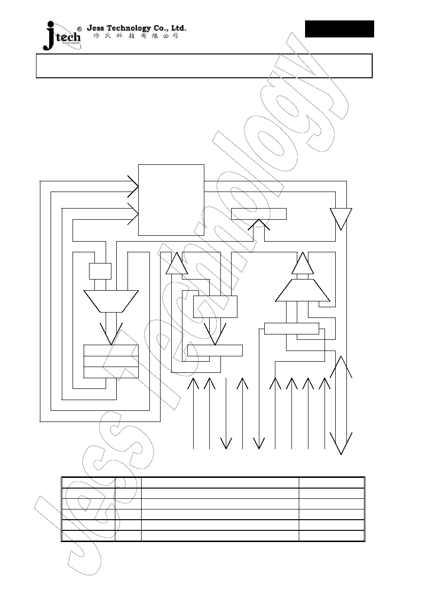
6.
Function Block Diagram
Several registers are used in the interface logic. The functions of the registers are described below
and their initial values are as indicated in the following table.
FDIN[7..0]
TP[21..0]
TPP
TPH
TPL
FDOUT[7..0]
FLASH
Memory
+ 1
MUX
CHKSUM
XOR
MODE
D[7..0]
S2P
MUX
SDI
SDO
R_Wn
SCLK/Strobe
Busy
P_Sn
D_Cn
CS1
CS0n
The Table Pointer register keeps the address of FLASH memory being written to or read from. It
will automatically increment by one at the completion of each read/write access.
Register
Type Description
Initial Value
TPL
W
Address register 0 for A7 ~ A0
"--------"
TPH
W
Address register 1 for A15 ~ A8
"--------"
TPP
W
Address register 2 for A21 ~ A16
"------"
Mode
W
Mode Control Register
"-----000"
Checksum
R
XOR checksum of data
"--------"