 | –≠–ª–µ–∫—Ç—Ä–æ–Ω–Ω—ã–π –∫–æ–º–ø–æ–Ω–µ–Ω—Ç: HF88M02 | –°–∫–∞—á–∞—Ç—å:  PDF PDF  ZIP ZIP |

Suites 2202-7, Tower 6, The Gateway,
9 Canton Road, Tsimshatsui,
Kowloon, Hong Kong
Tel: (852) 2123 3289 Fax: (852) 2123 3393
E-mail: sales@jesstech.com
Home Page: www.jesstech.com
HF88M02
Command Interface 2M-Bit Mask ROM with Expansion I/O
-1-
02/05/31
Product Name
Command Interface 2 M-Bit Mask ROM with Expansion I/O
Jtech Doc. No.
HF88M02
Jtech Product. No.
HF88M02
-
Table of Contents ≠
1
FUNCTION DESCRIPTION ...................................................................................................... 2
2
FEATURES ................................................................................................................................... 2
3
FUNCTIONAL BLOCK DIAGRAM ......................................................................................... 3
4 PIN DESCRIPTION..................................................................................................................... 4
4.1
P
AD
L
OCATION
.................................................................................................................. 5
4.2
P
AD
C
OORDINATION
.......................................................................................................... 6
5
DEVICE OPERATION ................................................................................................................ 7
5.1
R
ETRIEVE DATA IN
D
ATA
F
ILE
........................................................................................... 8
5.2
L
OADING THE
A
DDRESS
C
OUNTER
.................................................................................... 9
5.3
S
EQUENTIAL
R
EAD
M
ODE AND
A
UTO
I
NCREMENT OF
A
DDRESS
C
OUNTER
...................... 9
5.4
O
UTPUT DATA TO
E
XTERNAL
I/O..................................................................................... 10
5.5
R
EADING
I
NPUT PIN STATUS
............................................................................................. 10
5.6
R
ETRIEVING THE
C
ONTENTS OF
E
XPANSION
I/O
REGISTERS
............................................ 10
6
TIMING DIAGRAMS................................................................................................................ 11
D
ATA
F
ILE
R
EAD
C
YCLE
..................................................................................................................... 11
6.2
I
NTERRUPTED BY
I/O
WHEN
L
OADING
A
DDRESS
C
OUNTER
............................................ 11
6.3
S
ETTING AND
R
EADING THE
I/O M
ODE FOR
P0
AND
P1 .................................................. 12
6.4
R
EADING
P0
AND
P1
IN
M
IXED
-I/O M
ODE
..................................................................... 12
6.5
R
EADING THE INPUT PINS
................................................................................................ 12
6.6
O
UTPUT TO
P0
AND
P1 .................................................................................................... 13
7
ABSOLUTE MAXIMUM RATING........................................................................................ 144
8
AC ELECTRICAL CHARACTERISTICS.............................................................................. 14
9
DC ELECTRICAL CHARACTERISTICS.............................................................................. 15
10
APPLICATION CIRCUIT DIAGRAM............................................................................... 15

Suites 2202-7, Tower 6, The Gateway,
9 Canton Road, Tsimshatsui,
Kowloon, Hong Kong
Tel: (852) 2123 3289 Fax: (852) 2123 3393
E-mail: sales@jesstech.com
Home Page: www.jesstech.com
HF88M02
Command Interface 2M-Bit Mask ROM with Expansion I/O
-2-
02/05/31
1
Function Description
The HF88M02is a command interfaced 256K x 8 bit Mask ROM. It features command mode
interface with external CPU or MCU. In other words, it uses only 8-bit data bus and a few
additional control pins to load addresses and provide the ROM access as well as expansion I/O
ports capability. This design not only reduces pin count required to access data in ROM
dramatically but also allows for systems expansion to higher capacity memories while using the
existing board design. The application areas include voice, graphic, data storage in consumer
product.
2
Features
!
Data File Mode with only 11 pin interface
!
Sixteen-bit Expansion I/O pins with three-state mode
!
Voltage range 2.4V ~ 5.5V
!
Organization
-
Memory Cell Array: 256K x 8
!
Sequential Read Operation in Data File Operation Mode
-
Sequential Access : 120ns (min.) at V
DD
= 5.0V
!
Command/Address/Data Multiplexed I/O port
!
Low Operation Current (Typical)
-
10
µ
A Standby mode Current
-
10mA Active Read Current
!
Package bare chip, PLCC32
Suites 2202-7, Tower 6, The Gateway,
9 Canton Road, Tsimshatsui,
Kowloon, Hong Kong
Tel: (852) 2123 3289 Fax: (852) 2123 3393
E-mail: sales@jesstech.com
Home Page: www.jesstech.com
HF88M02
Command Interface 2M-Bit Mask ROM with Expansion I/O
-3-
02/05/31
3
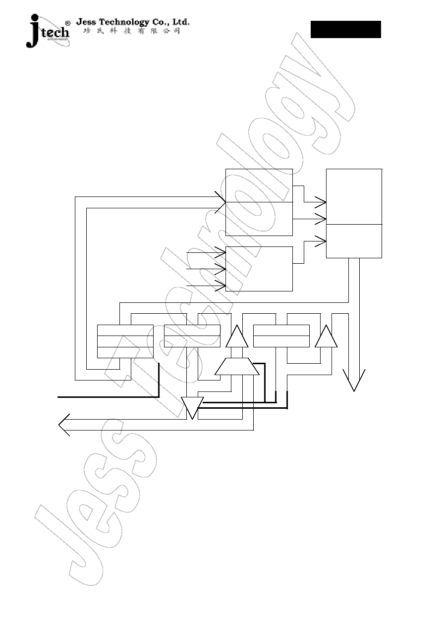
Functional block diagram
[AC18..A0]
X BUFFER &
DECODER
WEn
[P00..P07]
[P10..P17]
AC0
P0
AC2
OEn
MEMORY
CELL
ARRAY
CEn
DIR1
AC1
RS2..RS0
P1
Y BUFFER &
DECODER
[D7.. D0]
DIR0
CONTROL
LOGIC
SENSE
AMP.

Suites 2202-7, Tower 6, The Gateway,
9 Canton Road, Tsimshatsui,
Kowloon, Hong Kong
Tel: (852) 2123 3289 Fax: (852) 2123 3393
E-mail: sales@jesstech.com
Home Page: www.jesstech.com
HF88M02
Command Interface 2M-Bit Mask ROM with Expansion I/O
-4-
02/05/31
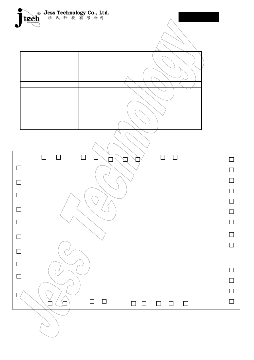
4
Pin Description
Symbol
Pin No. I/O
Description
VDD
32
P Positive power supply input pin.
VSS
16
P Gound pin.
CEn
22
I
The CEn (Chip Enable) input is the device selection and
power control for internal Mask ROM array. Whenever
CEn goes high, the internal Mask ROM will enter standby
(power saving) mode and accesses to internal registers are
inhibited. Otherwise, it is in active mode and the
contents of the ROM and registers can be accessed.
Please note that only accesses to the internal registers are
inhibited, but the status of I/O registers are not affected by
the CEn pin and will remain unchanged. CEn is also
useful to uniquely select a certain device for applications
where multiple-chip array is required.
WEn
1
I
WEn controls writing to internal registers such as the
Output Port Registers, Direction Registers, Address
Counter and Data on D7 ~ D0 are latched on the rising
edge of the WE pulse. The WEn (Write Enable) input is
internally pulled-up to VDD to prevent pin floating. So
this pin should stay at `1' state when inactive to prevent
unintended current consumption.
OEn
24
I
OEn (Output Enable) is the output control which gates
ROM array data, expansion I/O ports, Direction Registers
to the data I/O pins D7 ~ D0. The internal Address
Counter will automatically increment by one with each
rising edge of OEn pin in Sequentially Read mode.
HF88M02-PLCC32
11
2
9
8
7
6
5
4
29
28
24
27
3
30
31
2
23
25
13
14 15
18 19
20
21
22
32
16
1
12
17
26
P01
P02
P03
P04
P05
P06
P07
P1
4
P16
P15
OE
P10
P1
7
RS
1
RS
2
RS
0
P12
P13
D0
D1 D2
D4 D5
D6
D7
CE
VD
D
VS
S
WE
P00
D3
P11
Suites 2202-7, Tower 6, The Gateway,
9 Canton Road, Tsimshatsui,
Kowloon, Hong Kong
Tel: (852) 2123 3289 Fax: (852) 2123 3393
E-mail: sales@jesstech.com
Home Page: www.jesstech.com
HF88M02
Command Interface 2M-Bit Mask ROM with Expansion I/O
-5-
02/05/31
RS2~RS0
I
Register Select pins RS2 ~ RS0 for accessing ROM data,
Address Counter, as well as expansion I/O ports. The RS2
(Register Select) input is internally pulled-down to
Ground. So this pin should stay at `0' state when
inactive to prevent unintended current drain.
P17 ~ P10
I/O Bi-directional I/O port P1.
P07 ~ P00
I/O Bi-directional I/O port P0.
D7 ~ D0
21 ~ 17,
15 ~13
IO The Bi-directional Data I/O pins are used to input Starting
Address, setting the Expansion I/O direction and Output
Registers, and to output ROM array data during read
operations, contents of I/O Registers and status of input
pins. The D7 ~ D7 float to high-impedance when the chip
is deselected (CEn high) or when the outputs are disabled.
4.1
Pad Location
VSS
D6
RS0
P00
D1
D5
CEN
P04
NC
WEN
P05
D3
D0
VDD
D4
P12
P01
P10
P16
P06
P14
OEN
P07
VDD
VSS
P17
P15
NC
P11
P03
RS1
RS2
D2
P13
NC
VDD
P02
D7
NC
NC
VSS