
1
DESCRIPTION
The WT5041 is a high-performance, low-cost, CMOS 8-bit single-chip micro controller with on-chip OP Amp (OPA)
for heart rate detect and 128 segments LCD driver. This chip can be used dedicate for applications where heart rate
and LCD display are required, for example sports bicycle meter, heart rate meter and heart rate watch.
This chip has 8-bit CPU, RAM, ROM, I/Os, one 16-bit timer/counters, dual 8-bit timer interrupt controller, three 8-bit
PWM D/A output, resister to frequency converter (RFC), heart rate detect circuits, and a LCD driver. To be suitable
for portable battery-powered applications, a power saving function is included.
FEATURES
8-bit single chip micro controller with 8Kbytes ROM and 256 Bytes SRAM
Wide voltage operating range from 2.4 V to 5.5 V
Built-in 32.768KHz OSC circuits.
14 interrupt sources, 14 halt mode release sources (warm start), 8 off mode wake up sources (cold start); all sources
have independent latches each and multi-control is available.
I/O port (32 pins)
I/O porto 8 pins (shared with SEG25-SEG32)
I/O port1 1 pin (shared with OP Amp 1 pins)
I/O port1 3 pins (shared with PWM0~2 output)
I/O port1 4 pins (shared with RFC 4 pins)
IlO port2 8 pins (shared with key detect & event counter
I/O port3 6 pins (shared with OP Amp 6 pins)
I/O port3 2 pins (shared with BUZ/BUZB output)
~ Providing standby mode
Key wake up function
Build-in heart rate detect circuits and one 16-bit counter
Build-in RFC circuit and one 16-bit counter for thermistor and humidity sensor use.
Dual 8-bit timer & one 16-bit timedcounters
3 Channel 8-bit PWM output
LCD driver
LCD direct drive (max. 16-digit display at 1/4 duty)
1/4, 1/3, 1/2 duties and 1/2, 1/3 biases can be selected by software programming
1/4, 1/3, 1/2 duties and 1/2, 1/3 biases can be selected by software programming
LCD segments SEG25~32 can be used as 8 I/O pins by software programming
Real-time emulator
Package: Die form
2
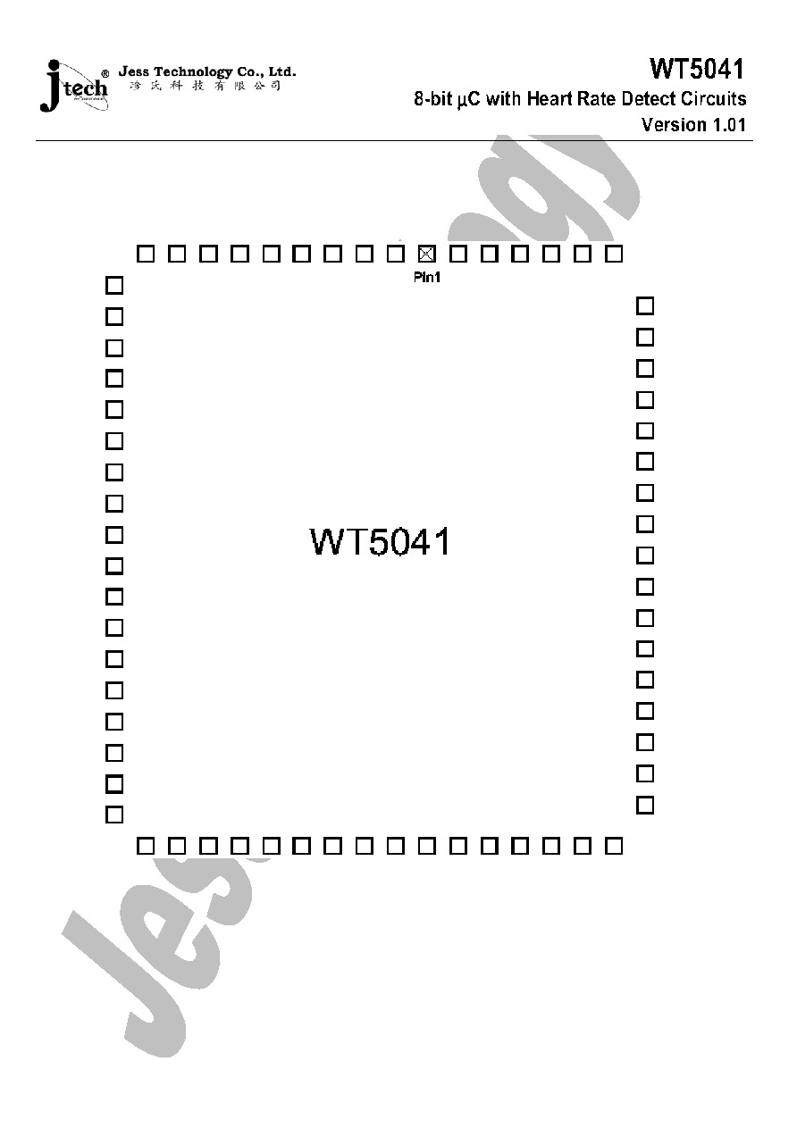
PAD LAYOUT

3
BLOCK DIAGRAM

4
PIN FUNCTION
Name
No.
I/O
Description
COM1
1
O
LCD common1
COM2
2
O
LCD common2
COM3
3
O
LCD common3
COM4
4
O
LCD common4
SEG1
5
O
LCD segment1
SEG2
6
O
LCD segment2
SEG3
7
O
LCD segment3
SEG4
8
O
LCD segment4
SEG5
9
O
LCD segment5
SEG6
10
O
LCD segment6
SEG7
11
O
LCD segment7
SEG8
12
O
LCD segment8
SEG9
13
O
LCD segment9
SEG10
14
O
LCD segment10
SEG11
15
O
LCD segment11
SEG12
16
O
LCD segment12
SEG13
17
O
LCD segment13
SEG14
18
O
LCD segment14
SEG15
19
O
LCD segment15
SEG16
20
O
LCD segment16
SEG17
21
O
LCD segment17
SEG18
22
O
LCD segment18
SEG19
23
O
LCD segment19
SEG20
24
O
LCD segment20
SEG21
25
O
LCD segment21
SEG22
26
O
LCD segment22
SEG23
27
I/O
LCD segment23
SEG24
28
I/O
LCD segment24
P00/SEG25
29
I/O
I/O port 00 or LCD segment 25
P01/SEG26
30
I/O
I/O port 01 or LCD segment 26
P02/SEG27
31
I/O
I/O port 02 or LCD segment 27
P03/SEG28
32
I/O
I/O port 02 or LCD segment 28
P04/SEG29
33
I/O
I/O port 04 or LCD segment 29
P05/SEG30
34
I/O
I/O port 05 or LCD segment 20
P06/SEG31
35
I/O
I/O port 05 or LCD segment 31
P07/SEG32
36
I/O
I/O port 07 or LCD segment 32
P30/IN1
37
I/O
I/O port 30 or OP function Input1
P31/IN2
38
I/O
I/O port 31 or OP function Input2
P32/IN3
39
I/O
I/O port 32 or OP function Input3
P33/O1
40
I/O
I/O port 33 or OP function Output1
P34/O2
41
I/O
I/O port 34 or OP function Output2
P35/O3
42
I/O
I/O port 35 or OP function Output3
P36/BUZ
43
I/O
I/O port 36 or OP function Output3
P37/BUZB
44
I/O
I/O port 37 or BUZZERB function
P20/INT0
45
I/O
I/O port 20 or INT/wake up input 0 pull high.negative edge trigger.

5
P21/INT1
46
I/O
I/O port 21 or INT/wake up input 1 pull high.negative edge trigger.
P22/INT2
47
I/O
I/O port 22 or INT/wake up input 2 pull high.negative edge trigger.
P23/INT3
48
I/O
I/O port 23 or INT/wake up input 3 pull high.negative edge trigger.
P24/INT4
49
I/O
I/O port 24 or INT/wake up input 4 pull high.negative edge trigger.
P25/INT5
50
I/O
I/O port 25 or INT/wake up input 5 pull high.negative edge trigger.
Name
No.
I/O
Description
P26/INT6
51
I/O
I/O port 26 or INT/wake up input 6 pull high.negative edge trigger.
P27/INT6/CNT
52
I/O
I/O port 27 or INT/wake up input 7/counter input
GND
53
P
Ground (0V)
XTAL2
54
I/O
32768 Hz crystal oscillator
XTAL1
55
I
32768 Hz crystal oscillator
P10/PWM0
56
I/O
I/O port 10.or PWM0 output
P11/PWM1
57
I/O
I/O port 11.or PWM1 output
P12/PWM2
58
I/O
I/O port 12.or PWM2 output
P13/VR
59
I/O
I/O port 13. OP reference voltage output
P14/RA
60
I/O
I/O port 14 or RFC R thermistor
P15/RB
61
I/O
I/O port 15 or RFC R humidity sensor
P16/RS
62
I/O
I/O port 16 or RFC R standrad
P17/CA
63
I/O
I/O port 17 or RFC Capacitor
/RESET
64
I
Reset. Internal pull high, active low.
BIAS1
65
O
LCD bias voltage 1
BIAS2
66
O
LCD bias voltage 2
VDD
67
P
Power supply.