1
DESCRIPTION
The WT5053 is a high-performance, low-cost, CMOS 8-bit single-chip microcontroller with 4KBytes on-chip ROM and an 8-
channel 12-bit analog to digital converter. This chip is suitable for variable applications, especially where analog signal
(sensor output) to digital signal conversion is required, including industrial control, consumer, communications, and security
products.
This chip has 8-bit CPU, RAM, ROM, I/Os, dual 16-bit timer/counters, interrupt controller, and an 8-channel 12-bit A/D
converter. To be suitable for portable battery-powered applications, a power saving function is included.
FEATURES
8-bit single chip microcontroller with 4Kbytes ROM and 128bytes SRAM
Wide voltage operating range from 2.4 V to 5.5 V
On-chip RC oscillator runs at 2MHz and crystal oscillator can run up to 8.0 MHz
6 interrupt sources (external: 1; internal:5); all sources have independent latches each
multiple interrupt control is available
I/O port (12 pins)
Port PO 8 pins (shared with analog inputs;
Port P1 4 pins (20mA sink current)
Operating current 2mA/4MHz~5V; providing standby mode (OSC is stopped and current
consumption < 1 uA~5V)
Watchdog timer
Dual PWM
Dual 16-bit timer/counters
A/D converter module
8 analog inputs multiplexed into one A/D converter
Sample and hold
20 [tS conversion time/per channel
12-bit resolution with +2 LSB accuracy
External reference input, AD
VRF
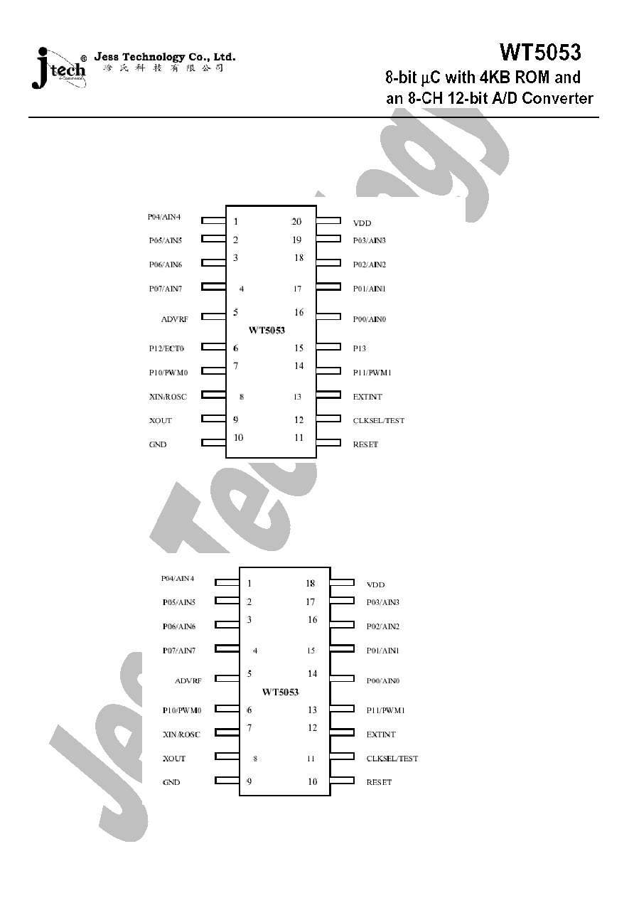
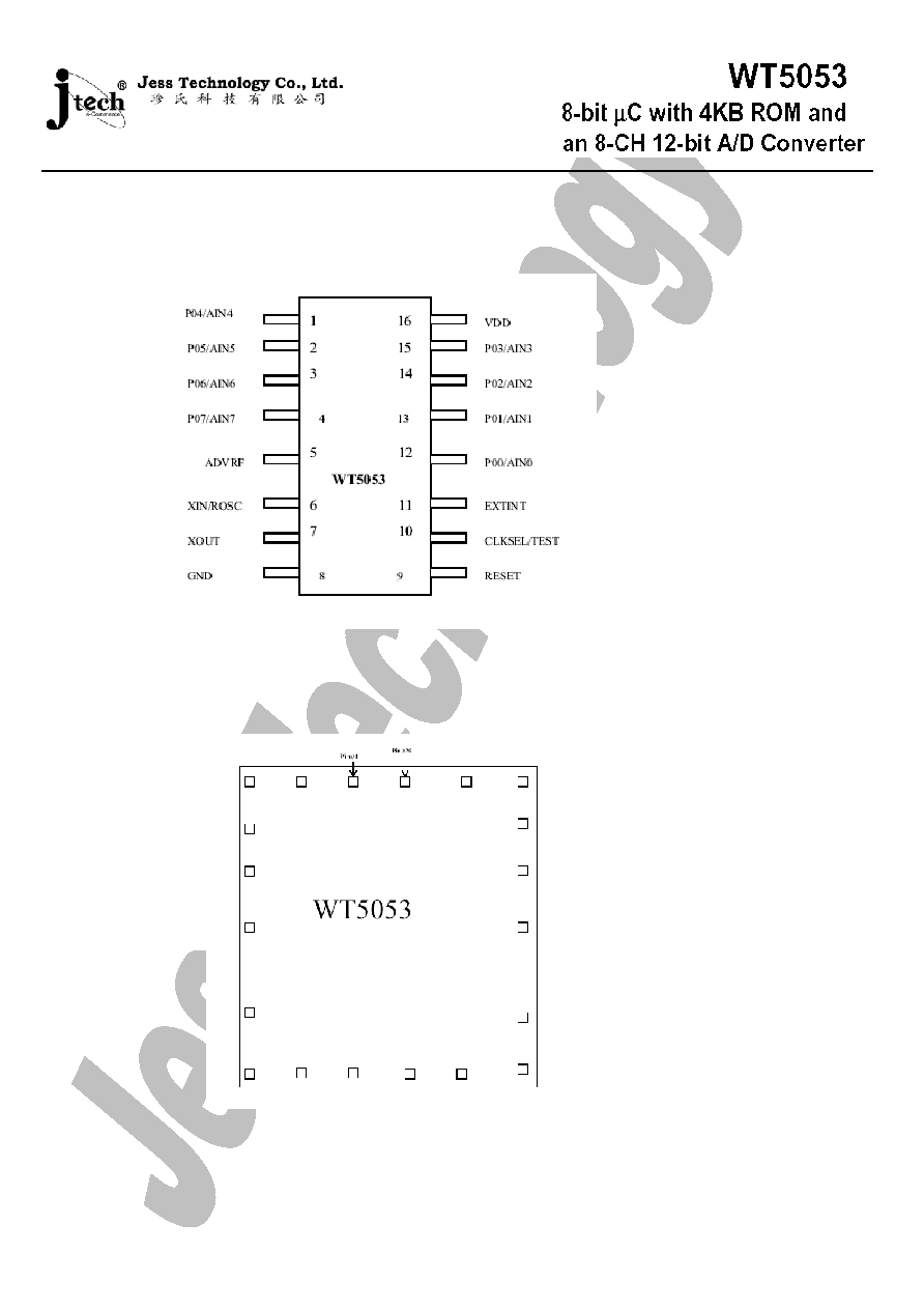
Package: Chip form, or 20/18/16-pin PDIP/SOP
5
PIN FUNCTION
PIN NAME
20-pin (18-pin) [16-pin]
In/Out
FUNCTIONS
P00/AIN0 ~ P03/AIN3
P04/AIN4 ~ P07/AIN7
16 ~19 (14~17) [12~15]
1~4 (1~4) [1~4]
I/O
8-bit I/O port; Internal pull-up;
o/p: sink 20mA(P04~P07); i/p: external pull-low
P10/PWM0
P11/PWM1
P12/ECT0
P13
7 (6) [X]
14 (13) [X]
6 (X) [X]
15 (X) [X]
I/O
(PWM0 output)
(PWM1 output)
(External counter input)
4-bit I/O port; internal pull-up;
o/p: sink 20mA; i/p: external pull-low
XIN/ROSC
8 (7) [6]
Input
Crystal input/ROSC input
XOUT
9 (8) [7]
Output
Crystal output
RESET
11 (10) [9]
Input
System reset signal input; low active
VDD
20 (18) [16]
Input
Power source
GND
10 (9) [8]
Input
Ground
AD
VRF
5 (5) [5]
Input
Reference voltage input to A/D
EXTINT
13 (12) [11]
Input
External interrupt input
CLKSEL/TEST
12 (11) [10]
Input
Clock sources select, connected to VDD for
ROSC or to GND for Crystal (Test Pin)
FUNCTION DESCRIPTION
[ 1 ] I/O PORTS
The WT5053 has 2 ports (12 pins) each as follows:
o P00 - P07 ; 8-bit FO port (shared with analog input AIN0-AIN7)
o P 10 - P 13 ; 4-bit I/O port (shared with PWM0/PWM 1, ECT0)
< 1 > Port P0 (P00 ≠P07)
Port P0 is an 8-bit bi-directional I/O port and its Data Register and Direction Control Register are located in P0DR ($00) and
P0DCR ($26), respectively. All port pins have individually selectable pull-up resistors, and among them, P04-P07 output
buffers are designed to have the capability to sink 20mA and thus can drive LED directly.
Port P0 pins are shared with analog inputs (in this case, P0x must be configured as input). When used as digital I/O pins, then
P0x is configured as output pin if P0DCRx is set to "1"; otherwise, if P0DCRx is cleared to "0", then P0x is configured as an
input pin. For more detail about the P0 port configuration, please refer to Table 1.
Note: When pins of port P0 are used as inputs and externally pulled low, then they will source current if the internal pins
are pulled up.
1.1 Port P0 Data Register (P0DR; $00); RJW; Initial value 00H
B7
B6
B5
B4
B3
B2
B1
B0
P0DR7
P0DR6
P0DR5
P0DR4
P0DR3
P0DR2
P0DR1
P0DR0