 | –≠–ª–µ–∫—Ç—Ä–æ–Ω–Ω—ã–π –∫–æ–º–ø–æ–Ω–µ–Ω—Ç: WT5058 | –°–∫–∞—á–∞—Ç—å:  PDF PDF  ZIP ZIP |

1
DESCRIPTION
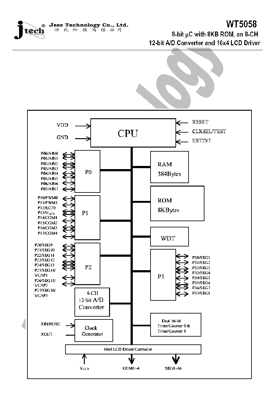
The WT5058 is a high-performance, low-cost, CMOS 8-bit single-chip microcontroller with 8Kbytes on-chip ROM, an 8-
channel 12-bit analog to digital converter and 16x4 LCD driver. This chip is suitable for variable applications, especially
where analog signal (sensor output) to digital signal conversion and LCD display are required, including industrial control,
consumer, communications, and security products.
This chip has 8-bit CPU, RAM, ROM, I/Os, dual 16-bit timer/counters, 16x4 LCD driver and an 8-channel 12-bit A/D
converter. To be suitable powered applications, a power saving function is included.
FEATURES
8-bit single chip microcontroller with 8K bytes ROM and 384bytes SRAM
Wide voltage operating range from 2.4 V to 5.5 V
On-chip RC oscillator runs at 2MHz and crystal oscillator can run up to 6.0 MHz
6 interrupt sources (external:l; internal:5); all sources have independent latches each and multiple interrupt control is
available
I/O port (32 pins)
Port PO 8 pins (shared with analog inputs;
Port P1 8 pins (20 mA sink current)
Port P2 8 pins (shared with SEG9-SEG16)
Port P3 8 pins (shared with SEG1-SEG8)
Interval Timer (Internal time base generator)
Operating current 2mA/4MHz@5V; providing standby mode (OSC is stopped and current consumption
<1uA@5V) and key wake-up mode
Watchdog timer
Dual PWM
Dual 16-bit timer/counters
A/D converter module
8 analog inputs multiplexed into one A/D converter
Sample and hold
20 S conversion time/per channel
12-bit resolution with ±2 LSB accuracy
External reference input, ADv~
LCD driver (automatically display)
LCD direct drive (max. 8-digit display at 1/4 duty)
1/4, 1/3, 1/2 duties and 1/2, 1/3 biases can be selected by programming
Package: Chip form, 28/40-pin PDIP or 28-pin Skinny

2
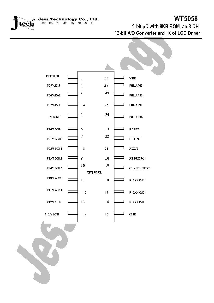
PACKAGE PIN ASSIGNMENT (40-PIN DIP)
3
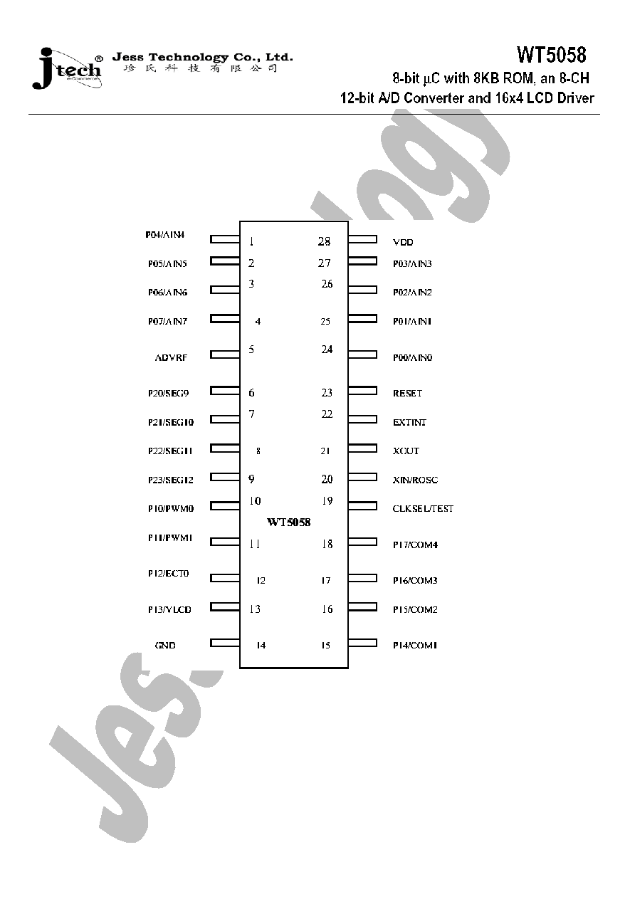
PACKAGE PIN ASSIGNMENT (28-PIN DIP or 28-PIN SKINNY; Option #1)
4
PACKAGE PIN ASSIGNMENT (28-PIN DIP or 28-PIN SKINNY; Option #2)
5
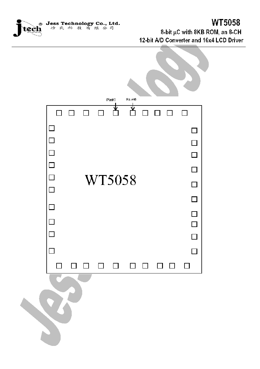
PAD LAYOUT (CHIP FORM)
6
BLOCK DIAGRAM

7
PIN FUNCTION
PIN NAME
40-pin
In/Out
FUNCTIONS
P00/AIN0- P03/AIN3
P04/AIN4-P07/AIN7
36-39
1-4
I/O
8-bit I/O port; internal pull-up;
o/p: sink 20mA(P04~P07); i/p: external pull-low
(shared with analog inputs)
P 10/PWM0
P11/PWM1
P 12/ECT0
P 13/VLCD
P 14/COM 1
P 15/COM2
P 16/COM3
P 17/COM4
16
17
18
19
21
22
23
24
I/O
(shared with PWM output); 8-bit I/O port; internal pull- up; o/p: sink
20mA; i/p: external pull-low
(Extemal counter)
(Bias voltage to LCD)
(LCD common output)
(LCD common output)
(LCD common output)
(LCD common output)
P20/SEG9
P21/SEG10
P22/SEG11
P23/SEG12
P24/SEG13
P25/SEG14/VCAP 1
P26/SEG15/VCAP2
P27/SEG 16/VCAP3
6
7
8
9
10
11
12
13
I/O
8-bit I/O port; internal pull-up; i/p: external pull-low
(shared with LCD segment output)
P20-P23 support key wake-up
P30/SEG1
P31/SEG2
P32/SEG3
P33/SEG4
P34/SEG5
P35/SEG6
P36/SEG7
P37/SEG8
30
31
32
33
34
35
14
15
I/O
8-bit I/O port; internal pull-up; i/p: external pull-low
(shared with LCD segment output)
XIN/ROSC
26
Input
Crystal input/ROSC input
XOUT
27
Output
Crystal output
RESET
29
Input
System reset signal input; low active
VDD
40
Input
Power source
GND
20
Input
Ground
AD
VRF
5
Input
Reference voltage input to A/D
EXTINT
28
Input
External interrupt input
CLKSEL/TEST
25
Input
Clock sources select, connected to VDD for ROSC or to GND for
Crystal (Test Pin)
8
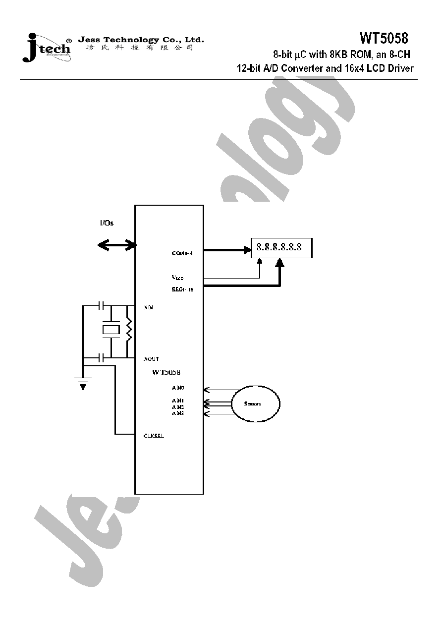
APPLICATION DIAGRAM
9
FUNCTION DESCRIPTION
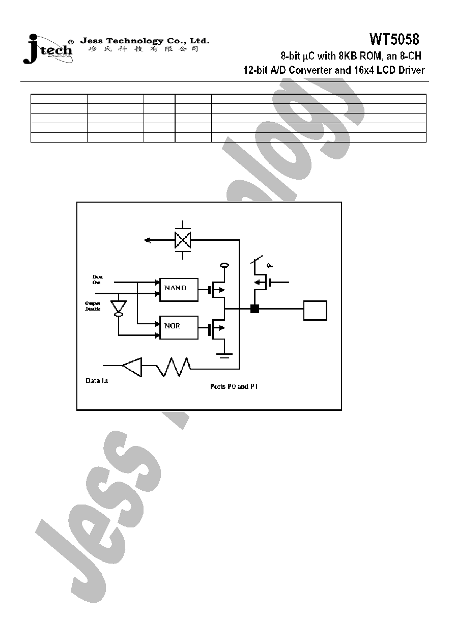
[ 1 ] I/O PORTS
The WT5058 has 4 ports (32 pins) each as follows:
P00 - P07 ; 8-bit I/O port (shared with analog input AIN0-AIN7)
P10 - P17 ; 8-bit I/O port (shared with PWM0/PWM1, COM1-4, ECT0,VLcD)
P20 - P27 ; 8-bit I/O port (shared with SEG9-16)
P30 - P37 ; 8-bit I/O port (shared with SEG1-8)
< 1 > Port PO (P00 -P07)
Port P0 is an 8-bit bi-directional I/O port and its Data Register and Direction Control Register are located in P0DR ($00) and
P0DCR ($26), respectively. All port pins have individually selectable pull-up resistors, and among them, P04~P07 output
buffers are designed to have the capability to sink 20mA and thus can drive LED directly.
Port P0 pins are shared with analog inputs (in this case, P0x must be configured as input). When used as digital I/O pins, then
P0x is configured as output pin if P0DCRx is set to "1"; otherwise, if P0DCRx is cleared to "0", then P0x is configured as an
input pin. For more detail about the P0 port configuration, please refer to Table 1.
Note: When pins of port P0 are used as inputs and externally pulled low, then they will source current If the internal pins
are pulled up.
1.1 Port PO Data Register (PODR; $00); R/W; Initial value 00
H
B7
B6
B5
B4
B3
B2
B1
B0
P0DR7
P0DR6
P0DR5
P0DR4
P0DR3
P0DR2
P0DR1
P0DR0
1.2 Port PO Data Direction Control Register (PODCR; $26); R/W Initial value 00
H
B7
B6
B5
B4
B3
B2
B1
B0
P0DCR7
P0DCR6
P0DCR5
P0DCR4
P0DCR3
P0DCR2
P0DCR1
P0DCR0
Table 1. Port P0 Configuration
10
P0DCR0 ~ 7
P0DR0 ~ 7
I/O
Pull-up
Results
0
0
In
No
Tri-state(Hi-Z)
0
1
In
Yes
P00 ~ P07 with pull-up resistor (MOS)
(NOTE)
1
0
Output
No
Output "0"
1
1
Output
No
Output "1"
< 2 > Port P1 (P10-P17)
Port P1 is an 8-bit bi-directional I/O port and its Data Register and Direction Control Register are located in P1DR ($01) and
P1DCR ($27), respectively. All port pins have individually selectable pull-up resistors and all their output buffers are
designed to have the capability to sink 20mA and thus can drive LED directly.
When used as digital I/O pins, then Plx is configured as output pin ifP1DCRx is set to 'T'; otherwise, if P1DCRx is cleared to
"0", then Pix is configured as input pin. For more detail about the configuration, please refer to Table 2.
Note: When pins of port P1 are used as inputs and externally pulled low, then they will source current if the internal pins
are pulled up.
2.1 Port P 1 Data Register (P 1 DR; $01); R/W; Initial value 00
H

11
B7
B6
B5
B4
B3
B2
B1
B0
P1DR7
P1DR6
P1DR5
P1DR4
P1DR3
P1DR2
P1DR1
P1DR0
2.2 Port P1 Data Direction Control Register(P1DCR; $27); R/W; Initial value 00H
B7
B6
B5
B4
B3
B2
B1
B0
P1DCR7
P1DCR6
P1DCR5
P1DCR4
P1DCR3
P1DCR2
P1DCR1
P1DCR0
Table 2: Port P1 Configuration
P1DCR0 ~ 7
P1DR0 ~ 7
I/O
Pull-up
Results
0
0
In
No
Tri-state(Hi-Z)
0
1
In
Yes
P10 ~ P17 with pull-up resistor (MOS)
(NOTE)
1
0
Output
No
Output "0"
1
1
Output
No
Output "1"
< 3 > Port P2 (P20 - P27)
Port P2 is an 8-bit bi-directional I/O port and all port pins have individually selectable pull-up resistors. The Data Register
and Direction Control Register of port P2 are located in P2DR ($02) and P2DCR ($28), respectively.
When used as digital I/O pins, then P2x is configured as an output pin if P2DCRx is set to "1"; otherwise, if P2DCRx is
cleared to "0", then P2x is configured as input pin. For more detail about the configuration of port P2, please refer to Table 3.
Note: When pins of port P2 are used as inputs and externally pulled low, then they will source current if the internal pins
are pulled up.
3.1 Port P2 Data Register (P2DR; $02) R/W; Initial value 00
H
B7
B6
B5
B4
B3
B2
B1
B0
P2DR7
P2DR6
P2DR5
P2DR4
P2DR3
P2DR2
P2DR1
P2DR0
3.2 Port P2 Data Direction Control Register(P2DCR; $28); R/W; Initial value 0OH
B7
B6
B5
B4
B3
B2
B1
B0
P2DCR7
P2DCR6
P2DCR5
P2DCR4
P2DCR3
P2DCR2
P2DCR1
P2DCR0
Table 3: The Configuration of port P2
P2DCR0 ~ 7
P2DR0 ~ 7
I/O
Pull-up
Results
0
0
In
No
Tri-state(Hi-Z)

12
0
1
In
Yes
P20 ~ P27 with pull-up resistor (MOS)
(NOTE)
1
0
Output
No
Output "0"
1
1
Output
No
Output "1"
< 4 > Port P3 (P30-P37)
Port P3 is an 8-bit bi-directional I/O port and all port pins have individually selectable pull-up resistors. The Data Register and
Direction Control Register of port P3 are located in P3DR ($03) and P3DCR ($29).
13
When used as digital I/O pins, then P3x is configured as output pin if P3DCRx is set to "1"; otherwise, if P3DCRx is cleared
to "0", then P3x is configured as input pin.
For more detail about the configuration of port P3, please refer to Table 4.
Note: When pins of port P3 are used as inputs and externally pulled low, then they will source current if the internal pins
are pulled up.
4.1 Port P3 Data Register (P3DR; $03); R/W; Initial value 00
H
B7
B6
B5
B4
B3
B2
B1
B0
P3DR7
P3DR6
P3DR5
P3DR4
P3DR3
P3DR2
P3DR1
P3DR0
4.2 Port P3 Data Direction Control Register (P3DCR; $29); R/W; Initial value 00
H
B7
B6
B5
B4
B3
B2
B1
B0
P3DCR7
P3DCR6
P3DCR5
P3DCR4
P3DCR3
P3DCR2
P3DCR1
P3DCR0
Table 4: The Configuration of Port P4
P3DCR0 ~ 7
P3DR0 ~ 7
I/O
Pull-up
Results
0
0
In
No
Tri-state(Hi-Z)
0
1
In
Yes
P30 ~ P37 with pull-up resistor (MOS)
(NOTE)
1
0
Output
No
Output "0"
1
1
Output
No
Output "1"
< 5 > PORTSEL ($11); R/W; Initial 00
H
B7
B6
B5
B4
B3
B2
B1
B0
CAPSEL
P3SCHN
P3SCLN
P2SCHN
P2SCLN
P1LCD
P1PWM1
P1PWM0
B7: CAPSEL; "1": external capacitors are connected to pins VCAP1, VCAP2, and VCAP3;
"0": I/O (P25~27) or SEG14~16 is selected
B6: P3SCHN; P3 segments or I/Os select (high nibble); 0: I/Os, 1: segments
B5: P3SCLN; P3 segments or I/Os select (low nibble); 0: I/Os, 1: segments
B4: P2SCHN; P2 segments or I/Os select (high nibble); 0: I/Os, 1: segments
B3: P2SCLN; P2 segments or I/Os select (low nibble); 0: I/Os, 1: segments
B2: P1LCD; LCD commons/ V
LCD
or I/Os select; 0: I/Os, 1: LCD commons/V
LCD
)
B1: P1PWM1; PWM1 or FO select; 0: FO, 1: PWM1 output
14
B0: P1PWM0; PWM0 or I/O select; 0: I/O, 1: PWM0 output
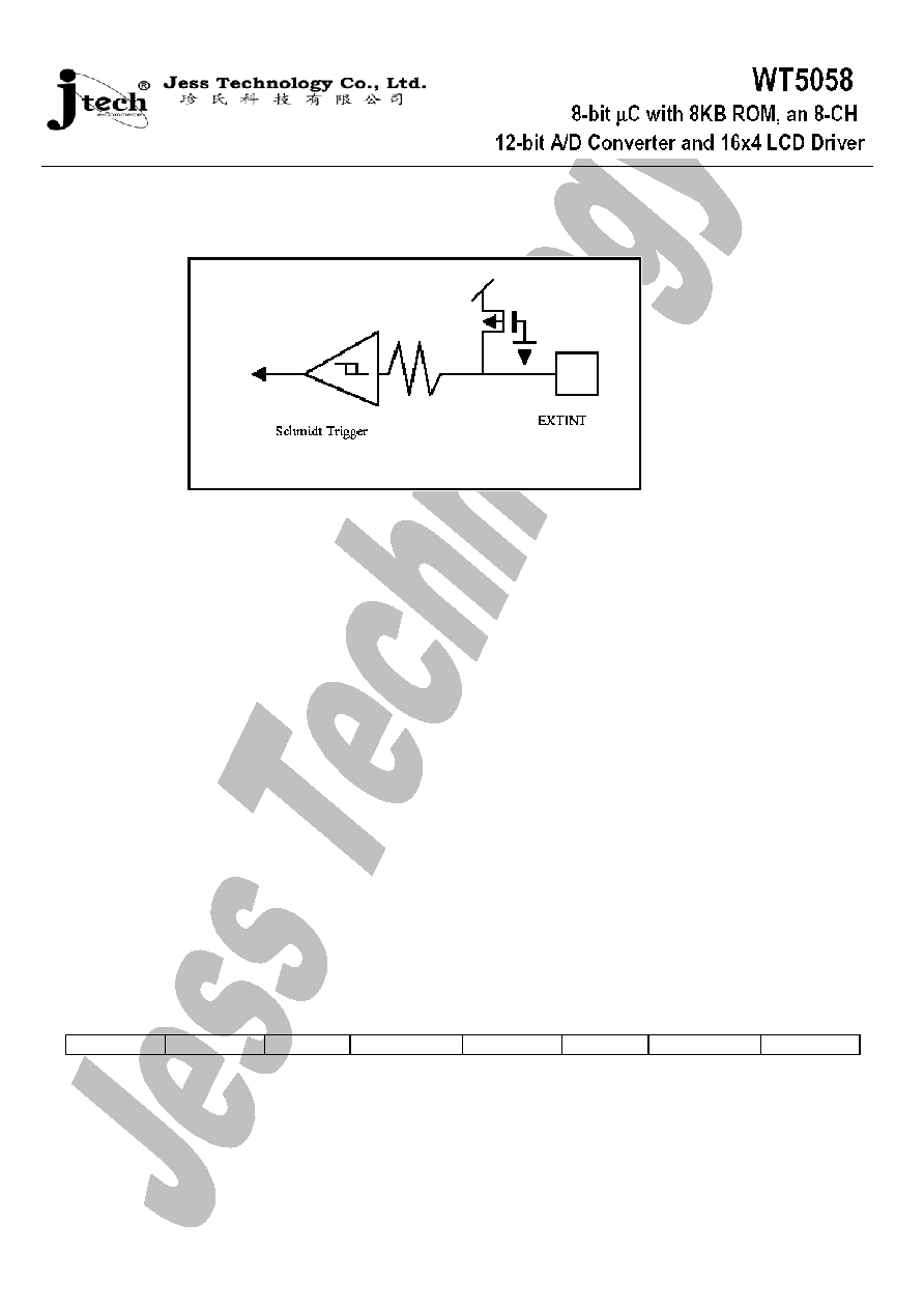
< 6 > EXTINT Input Pads
< 7 > NMI Source
INT 1 from T/C 1
< 8 > INT Sources
INT0 from T/CO
INT 1 from T/C 1
FQL INT
FQH INT
A/D conversion completion interrupt
EXTINT (rising edge)
[ 2 ] CLOCK SOURCE
CPU clock from RC oscillator: CLKSEL pin is connected to VDD
CPU clock from Crystal oscillator: CLKSEL pin is connected to GND
[ 3 ] TIMER/COUNTERS
CRYC register ($05); Oscillator control
B3-B0: R/W
B7
B6
B5
B4
B3
B2
B1
B0
--
--
--
RES/NORES
WUT1
WUT0
CRYST/PSM
ENAB
B0: ENAB; 0: enable (default), 1: disable
Note: b0 is set to 1 in normal operation, and can be set to 0 to stop the crystal (sleep mode)
B1: CRYST/PSM; 0: crystal starts (default), 1: power saving mode
Note: While crystal is being started (strong current mode), b1 is set to 0; once it starts, b1 can be set to 1 in order to switch the
crystal from "strong current mode" to "weak current mode" for power saving
15
B3: B2: WUT1: WUT0 (set the warm-up time at release of the hold operating mode)
00: 218/fc........... 65.5 ms (when fc=4MHz)
01: 214/fc............4.1 ms (when fc=4MHz)
10: reserved
00: 26/fc............16s(when fc=4MHz
B4: RES/NORES; 0: go through reset process, 1' without going through reset process, 1: without going through reset process
3.1 Timer/counters interrupt sources
INTC Register ($06); Interrupt control command register; R/W
Read: read interrupt flag
B7
B6
B5
B4
B3
B2
B1
B0
*
ADCI
FQHINT
EXTINT
T/C1NMI
T/C1INT
T/C0INT
FQLINT
Write: Interrupt enable/disable control
B7
B6
B5
B4
B3
B2
B1
B0
FUNCTION
*
*
*
*
*
*
*
*
Low frequency interrupt enable
*
*
*
*
*
*
*
*
Low frequency interrupt disable & clear
*
*
*
*
*
*
*
*
T/CO INT0 interrupt enable
*
*
*
*
*
*
*
*
T/CO INT0 interrupt disable & clear
*
*
*
*
*
*
*
*
T/C1 INT1 interrupt enable
*
*
*
*
*
*
*
*
T/C1 INT1 interrupt disable & clear
*
*
*
*
*
*
*
*
T/C 1 NMI interrupt enable
*
*
*
*
*
*
*
*
T/C1 NMI interrupt disable & clear
*
*
*
*
*
*
*
*
External interrupt (EXTINT)enable
*
*
*
*
*
*
*
*
External interrupt disable & clear
*
*
*
*
*
*
*
*
High frequency interrupt enable
*
*
*
*
*
*
*
*
High frequency interrupt disable & clear
*
*
*
*
*
*
*
*
A/D converter interrupt enable (hold & conversion start)
*
*
*
*
*
*
*
*
A/D converter interrupt disable & clear (sampling start)
3.2 TIMER/COUNTERS
WT5058 has two 16-bit timer/counters, namely T/CO and T/C 1, one low-frequency timer, and one high-frequency timer.
Both T/CO and T/C1 can be used as either a timer or a counter, and T/C 1 has auto-reload capability.
IN COUNTER MODE
16
If T/CO (T/C1) is used as an internal counter, by loading zero into register T/COH (T/C1H) and T/COL (T/C1L), the user can
reset the timer. When the specified timer is activated, the count value can be read from registers T/COH (T/C1H) & T/COL
(T/C1L) by reading registers T/COH (T/C1H) and then registers T/COL (T/C1L) will be latched automatically. While
writing registers T/COH (T/C1H) and T/COL (T/C1L), the register T/COL (T/C1L) must be written first and then followed by
writing T/COH (T/C1H). To guarantee correct counting, it is not allowed to write ONLY either T/C0H(T/C1H) or
T/C0L(T/C1L).
Registers for loading T/C0 & 1 16 bit data
LDT/C0($0A); Write
Load (&latch) T/C0 16-bit data
LDT/C1($0D); Write
Load (&latch) T/C1 16-bit data
T/C0 1 16-bit data locations
High Byte Data (D15 ~ D8)
Low Byte Data (D7 ~ D0)
T/C0
T/C0H ($0B); B7 ~ B0
T/C0H ($0C); B7 ~ B0
T/C1
T/C1H ($0E); B7 ~ B0
T/C1H ($0F); B7 ~ B0
TMC Register ($07); Timer control register, Write
B7
B6
B5
B4
B3
B2
B1
B0
T1AUTO
T1TCS2
T1TCS1
T1TCS0
--
T0TCS2
T0TCS10
T0TCS0
B3: reserved
B7: T/C1 Auto-reload selection (can be stop on-the-fly)
"0": disable; "1": enable
B2 ~ B0: T/C0 timer sources and timer/counter mode selection
T/C0 Clock Source Table
T0TCS2
T0TCS1
T0TCS0
Mode
Selected Source
0
0
0
Timer
CPU Clock (T)
0
0
1
Timer
T/4
0
1
0
Timer
T/8
0
1
1
Timer
T/16
1
0
0
Timer
T/32
1
0
1
Timer
T/64
1
1
0
Timer
T/128
1
1
1
Timer
External counter (ETC0)
B6 ~ B4: T/C1 timer sources and timer/counter mode selection
T/C1 Clock Source Table
17
T1TCS2
T1TCS1
T1TCS0
Mode
Selected Source
0
0
0
Timer
CPU Clock (T)
0
0
1
Timer
T/4
0
1
0
Timer
T/8
0
1
1
Timer
T/16
1
0
0
Timer
T/32
1
0
1
Timer
T/64
1
1
0
Timer
T/128
1
1
1
Timer
Clock source from T/C0 output
IN TIMER MODE
In regular timer mode, T/CO and T/C1 can be re-loaded and always counts down from the value set by the user. If the
specified bit is enabled in INTC register ($06) and the timer counts down from the value set by the user toward 0000H, then
once it hits 0000H and becomes underflow, an interrupt signal will be generated. The value set by the user will be re-loaded to
the timer automatically, and, again, the timer counts down from the value set by the user toward 0000
H
.
T/C1 IN PWM MODE
When the PWM mode is selected, T/C1 incorporated with the output compare registers OCR10 and OCR11 performs a dual 8,
9 or 10-bit, free-running, glitch-free and phase correct PWM with outputs on the P 10/PWM0 and P 11/PWM1 pins. The
PWM output frequency is depends on the resolutions, i.e., 8, 9, or 10-bit, and the OSC frequency, F
OSC
. Referring to Table 5
for more detail
In this mode T/C 1 acts as an up/down counter, counting up from 0000H to MAX and counts down again to zero before the
cycle is repeated. When the counter value matches the contents of the 10 least significant bits (for 10-bit PWM case) of
OCR10 or OCR11, the P10 (PWM0) / P11 (PWM1) pins are set or cleared according to the setting of the CPA0 or CPB0 bits
in the T/C1 control register TCCR10.
Write procedure for PWM operation should be OCR10L ($2B) first, followed by OCR10H ($2A), and then finally
TCCR10 ($10).
TCCR10 ($10); R/W; Initial value 00
H
.
B7
B6
B5
B4
B3
B2
B1
B0
--
CAP0
--
CPB0
--
--
PWMS1
PWMS0
PWMS 1
PWMS0
Description
0
0
PWM function is disable (default)
18
0
1
T/C 1 is an 8-bit PWM
1
0
T/C1 is a 9-bit PWM
1
1
T/C1 is a 10-bit PWM
CPA0/CPB0
Results on PWM0/PWM1
Up counting and output is cleared when compare match.
Down counting and output is set when compare match
Down counting and output is cleared when compare match.
Up counting and output is set when compare match
Table 5: The relationship between the PWM output frequency and its resolution
PWM Resolution
Timer MAX value
Frequency
8-bit
$00FF
Fosc/512
9-bit
$01FF
Fosc/1024
10-bit
$03FF
Fosc/2048
OCR 10H ($2A) / OCR10L ($2B); T/C 1 output compare register; R/W; Initial value 00
H
B7(MSB)
B6
B5
B4
B3
B2
B1
B0
B7
B6
B5
B4
B3
B2
B1
B0(LSB)
OCR11H ($2C)/OCR11L ($2D); T/C 1 output compare register; R/W; Initial value 00
H
B7(MSB)
B6
B5
B4
B3
B2
B1
B0
B7
B6
B5
B4
B3
B2
B1
B0(LSB)
To avoid the false counting of the PWM pulse in the event of abnormal OCR10/OCR11 write (glitch case), the
OCR10/OCRllcontents while being written, are copied to a temporary location and are latched when T/C1 reaches the value
MAX.
Note: The value in OCR10/OCRll can NOT be 0000H or MAX; The minimal value is 0001 H and the maximal
value is MAX-1.
WDTMR register ($12)
Watchdog timer must reset within TWDT seconds; otherwise the system will be reset.
B7
B6
B5
B4
B3
B2
B1
B0
FQHS2
FQHS1
FQHS0
--
WDTEN
WDTS2
WDTS1
WDTS0
B2:B0: Watchdog timer or FQL output frequencies select (f
WDT
)
OCR11H
OCR11L
OCR10H
OCR10L
19
WDTS2
WDTS1
WDTS0
Output Frequency (f
WDT
) ~OSC=4MHz
0
0
0
OSC1/2
17
(0.25Hz)
0
0
1
OSC1/2
16
(0.5Hz)
0
1
0
OSC1/2
15
(1.0Hz)
0
1
1
OSC1/2
14
(2.0Hz)
1
0
0
OSC1/2
13
(4.0Hz)
1
0
1
OSC1/2
12
(8.0Hz
1
1
0
O8C1/2
11
(16.0Hz)
1
1
1
OSC1/2
10
(32.0Hz)
Where OSC 1=OSC/2
7
, so when OSC=4MHz then OSC l=32KHz
B3: WDTEN: Watchdog timer/FQL select; 1: watchdog enable & FQL disable,
0:watchdog disable & FQL enable
B7: B5: FQHS2 ~ FQHS0; FQH output frequencies select
FQHS2
FQHS1
FQHS0
Output Frequency(@OSC=4MHz)
0
0
0
OSC1 (32kHz)
0
0
1
OSC1/2(16kHz)
0
1
0
OSC1/2
2
(8kHz)
0
1
1
OSC1/2
3
(4kHz)
1
0
0
OSC1/2
4
(2kHz)
1
0
1
OSC1/2
5
(1kHz)
1
1
0
OSC1/2
6
(512Hz)
1
1
1
OSC1/2
7
(256Hz)
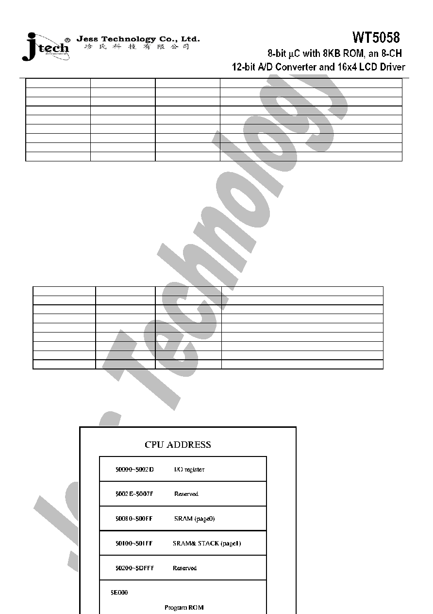
[ 4 ] MEMORY MAP
The following figure shows the location of memory mapping.

20
[ 5 ] CLOCK MODES
For portable battery-powered applications, stand-by mode is required for saving power. In this chip, by writing the SLPST
register ($09), user can stop the CPU clock such that CPU goes to stand-by mode.
The wake-up sources can be enable by setting the SLWC register ($08) (there are two sources in this chip, namely port P20-
P23 and FQL wake-ups). After receiving a wake-up signal, the CPU is reset.
SLWC register ($08); Sleep/wake-up control register; R/W
B7
B6
B5
B4
B3
B2
B1
B0
*
*
*
*
*
*
P2SC
FQLTBI
21
b1: P2SC: P20-P23 port keyboard state change
0: wake-up disable; 1: wake-up enable
b0: FQLTBI: FQL time base interrupt
0: wake-up disable; 1: wake-up enable
SLPST register ($09), Write
Write: Sleep start
To get into sleep mode, the program should be written as below(two consecutive instructions)
STA 08
H
STA 09
H
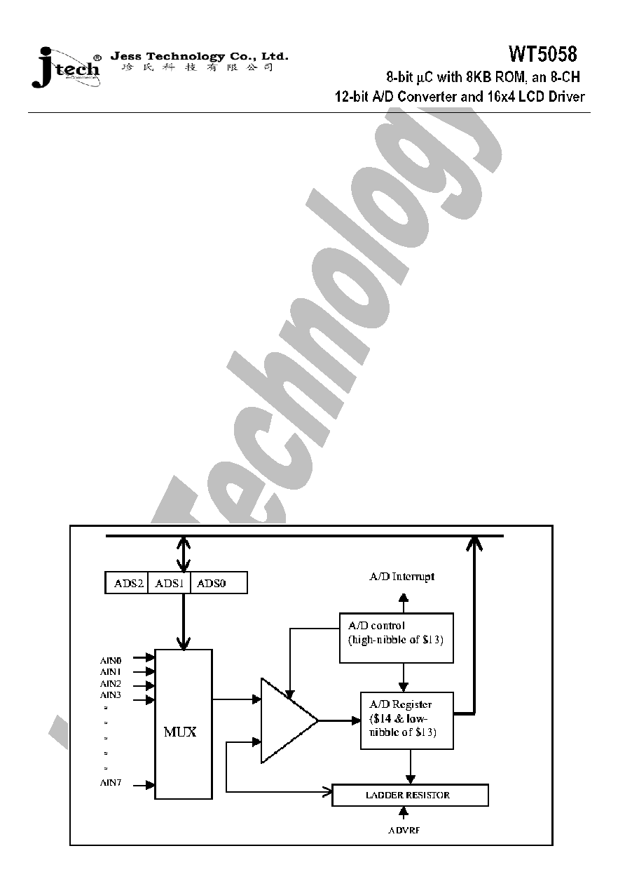
[ 6 ] A/DCONVERTER
A 12-bit successive approximation method used in this A/D converter, as shown in the following figure. By
multiplexing method, this A/D converter can manage up to eight analog inputs. A/D conversion is started by a write
operation to the analog input selection bit in the A/D control register and by selecting the analog voltage input pins.
When the conversion is completed, the A/D interrupt request bit in the interrupt request register is set. The result of
A/D conversion is stored in the A/D register. During A/D conversion stage, the A/D register must not be read,
otherwise the incorrect value may be obtained.
22
ADCR ($13): A/D control register;
b7: A/D On/Off control;
b7=0, A/D Off (default); b7=l, A/D On (write)
b3 :b0: High-nibble of A/D data
B7
B6
B5
B4
B3
B2
B1
B0
ADON
CKS1
CKS0
--
B3
B2/ADS2
B1/ADS1
B0/ADS0
CKS1
CKS0
Input Clock Selection
0
0
0
/4(when CPU clock is 1 MHz, this option is recommended)
0
1
0
/8 (when CPU clock is 2MHz, this option is recommended)
1
0
0
/16 (when CPU clock is 4 MHz, this option is recommended)
1
1
0
/32 (when CPU clock is 8MHz, this option is recommended)
*
0
represents CPU/System clock
ADS2
ADS1
ADS0
Input Selection
0
0
0
AIN0
0
0
1
AIN1
0
1
0
AIN2
0
1
1
AIN3
1
0
0
AIN4
1
0
1
AIN5
1
1
0
AIN6
1
1
1
AIN7
ADR ($14) :A/D register; Low Byte of A/D data (D7-D0; note: Dll-D8 in register ADCR ($13))
[ 7 ] LCD DRIVER/CONTROLLER
The WT5058 contains 64-segment LCD driver/controllers and it has circuit that directly drives the Liquid Crystal Display
(LCD) and its control circuit.
The WT5058 has the following connecting pins with
(1) Segment output; 16 pins (SEG1-SEG16)
(2) Common output; 4 pins (COM 1-COM4)
In addition, VCAP 1, VCAP2, VCAP3, and VLCD are bias voltage input pins to drive the LCD In power saving mode,
VCAP1, VCAP2 and VCAP3 should be connected with 0.01uF capacitors
The devices that can be directly driven is selected for LCD drivers of following drive methods
(1) 1/4 duty (1/3 bias) LCD; Max. 64 segments (8 segments X 8 digits)
(2) 1/3 duty (1/3 bias) LCD; Max. 48 segments (8 segments X 6 digits)
23
(3) 1/3 duty (1/2 bias) LCD; Max. 48 segments (8 segments X 6 digits)
(4) 1/2 duty (1/2 bias) LCD; Max. 32 segments (8 segments X 4 digits)
7.1 Control of LCD Driver
LCDC ($15); bl~b0, Write
B7
B6
B5
B4
B3
B2
B1
B0
*
*
*
LCDPS
LFS1
LFS0
DTY1
DTY0
DTY1
DTY0
Duty & Bias Selection
0
0
1/4 duty(l/3 bias)
0
1
1/3 duty (1/3 bias)
1
0
1/3 duty (1/2 bias)
1
1
1/2 duty(l/2 bias)
Note: Initial value: bl=0; b0=0
LFS1
LFS0
Select guide (frequency=64Hz)
When OSC 4MHz, this option is recommended
When OSC 8MHz, this option is recommended
When OSC 2MHz, this option is recommended
When OSC 1MHz, this option is recommended
LCDPS: "0": Normal mode
"1": Power saving mode
Note: Initially this system is in normal mode, once the LCD is lit then, after around 1 second, this system can be switched to
power saving mode for power saving. But, please be careful that the LCD can ONLY be turned on by using normal mode
(can't use power saving mode) when it being turned off and would like to turn it on again.
7.2 Frame Frequency
Base Freq. @64Hz
1/4 Duty
1/3 Duty
1/2 Duty
Frame Freq.
f= 256 Hz
f= 192 Hz
f= 128 Hz
7.3 LCD Drive Voltage
The LCD is on only when the difference in potential between the segment output and common output is + V
ON
or- V
ON
, and
turn off at all other cases, where V
ON
is the voltage value on V
LCD
pin. If CPU and LCD drive voltage are different, V
LCD
pin is
connected to VDD through a 100K ohm variable resister, R; otherwise, if CPU and LCD drive voltage are the same, V
LCD
pin
is connected to VDD directly. If V
R
is the voltage drop on R, then V
ON
=VDD-V
R
7.4 LCD Display Operation

24
The LCD driver generates the segment signals and common signals in accordance with display data and drive method. Thus,
display patterns can be changed easily by overwriting the contents of the display data area with a program.
DISPLAY DATA AREA
Write the following assigned area
SEG1-SEG8
SEG9-SEG16
COM1
DDA11 ($16)
DDA12 ($17)
COM2
DDA21 ($1A)
DDA22 ($1B)
COM3
DDA31 ($1E)
DDA32 ($1F)
COM4
DDA41 ($22)
DDA42 ($23)
1/4 DUTY
COM4
COM3
COM2
COM1
1/3 DUTY
****
COM3
COM2
COM1
1/2 DUTY
****
****
COM2
COM1
[ 8 ] I/O REGISTER SUMMARY
NAME
ADDR
R/W
D7
D6
D5
D4
D3
D2
D1
D0
P0DR
$00
R/W
P0DR7
P0DR6
P0DR5
P0DR4
P0DR3
P0DR2
P0DR1
P0DR0
P1DR
$01
R/W
P1DR7
P1DR6
P1DR5
P1DR4
P1DR3
P1DR2
P1DR1
P1DR0
P2DR
$02
R/W
P2DR7
P2DR6
P2DR5
P2DR4
P2DR3
P2DR2
P2DR1
P2DR0
P3DR
$03
R/W
P3DR7
P3DR6
P3DR5
P3DR4
P3DR3
P3DR2
P3DR1
P3DR0
Reserved
$04
--
--
--
--
--
--
--
--
--
CRYC
$05
R/W
--
--
--
RES/NO
RES
WUT1
WUT0
CRYST/
PSM
ENAB
INTC
$06
R/W
--
ADCI
FQHINT EXTINT T/C1N
MI
T/C1IN
T
T/C0IN
T
FQLINT
TMC
$07
W
T1AUT
O
T1TCS2
T1TCS1
T1TCS0
--
T0TCS2
T0TCS1
T0TCS0
SLWC
$08
R/W
--
--
--
--
--
--
P2SC
FQLTBI
SLPST
$09
W
--
--
--
--
--
--
--
--
LDT/C0
$0A
W
--
--
--
--
--
--
--
--
T/C0H
$0B
R/W
B7
B6
B5
B4
B3
B2
B1
B0
T/C0L
$0C
R/W
B7
B6
B5
B4
B3
B2
B1
B0
LDT/C1
$0D
W
--
--
--
--
--
--
--
--
T/C1H
$0E
R/W
B7
B6
B5
B4
B3
B2
B1
B0
T/C1L
$0F
R/W
B7
B6
B5
B4
B3
B2
B1
B0
TCCR10
$10
R/W
--
CPA0
--
CPB0
--
--
PWMS1
PWMS0
PORTSEL
$11
R/W
CAPSE
L
P3SCH
N
P3SCLN P2SCH
N
P2SCLN P1LCD
P1PWM
1
P1PWM
0
WDTMR
$12
W
FQHS2
FQHS1
FQHS0
--
WDTEN WDTS2
WDTS1
WDTS0
ADCR
$13
R/W
ADON
CKS1
CKS0
--
B3
B2/ADS
2
B1/ADS
1
B0/ADS
0
ADR
$14
R
B7
B6
B5
B4
B3
B2
B1
B0
LCDC
$15
W
--
--
--
LCDPS
LFS1
LFS0
DTY1
DTY0
25
DDA11
$16
W
B7
B6
B5
B4
B3
B2
B1
B0
DDA12
$17
W
B7
B6
B5
B4
B3
B2
B1
B0
Reserved
$18~19
W
--
--
--
--
--
--
--
--
DDA21
$1A
W
B7
B6
B5
B4
B3
B2
B1
B0
DDA22
$1B
W
B7
B6
B5
B4
B3
B2
B1
B0
Reserved
$1C~1D
W
--
--
--
--
--
--
--
--
DDA31
$1E
W
B7
B6
B5
B4
B3
B2
B1
B0
DDA32
$1F
W
B7
B6
B5
B4
B3
B2
B1
B0
Reserved
$20~21
W
--
--
--
--
--
--
--
--
DDA41
$22
W
B7
B6
B5
B4
B3
B2
B1
B0
DDA42
$23
W
B7
B6
B5
B4
B3
B2
B1
B0
Reserved
$24~25
P0DCR
$26
R/W
P0DCR7 P0DCR6 P0DCR5 P0DCR4 P0DCR3 P0DCR2 P0DCR1 P0DCR0
P1DCR
$27
R/W
P1DCR7 P1DCR6 P1DCR5 P1DCR4 P1DCR3 P1DCR2 P1DCR1 P1DCR0
P2DCR
$28
R/W
P2DCR7 P2DCR6 P2DCR5 P2DCR4 P2DCR3 P2DCR2 P2DCR1 P2DCR0
P3DCR
$29
R/W
P3DCR7 P3DCR6 P3DCR5 P3DCR4 P3DCR3 P3DCR2 P3DCR1 P3DCR0
OCR10H
$2A
R/W
B7
B6
B5
B4
B3
B2
B1
B0
OCR10L
$2B
R/W
B7
B6
B5
B4
B3
B2
B1
B0
OCR11H
$2C
R/W
B7
B6
B5
B4
B3
B2
B1
B0
OCR11L
$2D
R/W
B7
B6
B5
B4
B3
B2
B1
B0
[ 9 ] ELECTRICAL CHARACTERISTICS
ABSOLUTE MAXIMUM RATINGS (VSS=0V)
PARAMETER
SYMBOL
RATING
UNIT
DC Supply Voltage
VDD
< +
V
Input Voltage Range
Vin
-0.5 ~ VDD +0.5
V
Operating Temperature
Topr
0 ~ +70
Storage Temperature
Tstg
-50 ~ +150
ELECTRICAL CHARACTERISTICS (VSS = 0V, Topr = 0 to 70)
PARAMETER
SYMBOL
Min.
Typ.
Max.
Unit
CONDITIONS
Operating Voltage
VDD
2.4
--
5.5
V
Operating Current
I
OP
2
mA
OSC 4MHz @ 5.0V
Standby Current
I
STB
1.0
A
VDD=5.0V
OSC Frequency
F
OSC
6.0
MHz
VDD=5.0V
Input High Level
V
IH
4.0
2.5
V
VDD=5.0V
VDD=3.0V
Input Low Level
V
IL
0.8
0.5
V
VDD=5.0V
VDD=3.0V
P04 ~ P07 & Port1
Output High I (I/O)
I
OH
10
mA
VDD=5.0V
Voh=4.0V
P04 ~ P07 & Port1
Output Sink I (I/O)
I
OL
20
mA
VDD=5.0V
Vol=0.8V
Port 2& Port3
Output High I (I/O)
I
OH
4
mA
VDD=5.0V
Voh=4.0V
26
Port 2 & Port3
Output Sink I (I/O)
I
OL
4
mA
VDD=5.0V
Vol=0.8V
CPU Clock
F
CPU
0.03
6.0
MHz
F
CPU
= F
OSC
@5.0V
A/D CONVERSION CHARACTERISTICS (Topr = 0 to 70 )
PARAMETER
SYMBOL
CONDITIONS
Min.
Typ.
Max.
UNIT
Analog Reference Voltage
AD
VRF
3.0
--
AV
DD
V
Valid Voltage Range
V
RING
AD
VRF
=5V
0.5
4.0
V
Valid Voltage Range
V
RING
AD
VRF
=3V
0.5
2.0
V
Analog Input Voltage
AV
IN
AV
SS
--
AV
DD
V
Analog Supply Current
I
REF
--
0.5
1
mA
Input Impedance
Z
230
K
Differential nonlinear error
1
E
NL
±
1
LSB
Differential nonlinear error
2
E
INL
±
2
LSB
Offset error
3
E
OS
±
2
LSB
Absolute Error
4
E
ABS
VDD=5V, V
SS
=0V
AD
VRF
=5V, AV
SS
=0V
--
--
±
3
LSB
Conversion Time
T
CV
--
--
30
S
1. The differential nonlinear error (E
NL
) is the step width difference of the actual and the ideal transfer curves.
2. The integral nonlinear error (E
NL
) is the peak difference between the centers of the actual and the ideal transfer curves.
3. The offset error (E
OS
) is the absolute difference of the straight lines, which fit the actual and the ideal transfer curves.
4. The absolute error (E
ABS
) is the maximum difference between the center of the steps of the actual and the ideal transfer
curves for a non-calibrated ADC.