 | –≠–ª–µ–∫—Ç—Ä–æ–Ω–Ω—ã–π –∫–æ–º–ø–æ–Ω–µ–Ω—Ç: WT50F6 | –°–∫–∞—á–∞—Ç—å:  PDF PDF  ZIP ZIP |

WT50F6
8-bit
µC with 8KB ISP Flash Memory, 8-CH
12-bit A/D Converter and 16x4 LCD Driver
Preliminary
1 June/12/2001 Ver.1.10
DESCRIPTION
The WT50F6 is a high-performance, low-cost, CMOS 8-bit single-chip micro
controller with 8Kbytes in-system-programmable flash memory, an 8-channel 12-bit
rail-rail A/D converter and 16x4 LCD driver. This chip is suitable for variable
applications, especially where analog signal (sensor output) to digital signal
conversion, LCD display and short development cycle are required, including
industrial control, consumer, communications, and security products.
This chip has 8-bit CPU, RAM, flash memory, I/Os, dual 16-bit timer/counters;
interrupt controller, 16x4 LCD driver and an 8-channel 12-bit A/D converter. To be
suitable for portable battery-powered applications, a power saving function is
included.
FEATURES
8-bit single chip micro controller with 8K bytes flash memory and 384bytes
SRAM
Wide voltage operating range from 2.7 V to 5.5 V
On-chip RC oscillator runs at 8MHz and crystal oscillator can run up to 8.0 MHz
8 interrupt sources (external:2; internal:6) ; all sources have independent latches
each and multiple interrupt control is available
I/O port (32 pins)
Port P0 8 pins (shared with analog inputs)
Port P1 8 pins (P10~P13 25 mA source; P10~P17 25mA sink current)
Port P2 8 pins (shared with SEG9~SEG16)
Port P3 8 pins (shared with SEG1~SEG8)
Port P4 3 pins P42(output only ) share with CLKSEL
P41 share with EXTINT
P40 share with ADvrf
Interval Timer (Internal time base generator)
Operating current 2mA/4MHz@5V; providing standby mode (OSC is
stopped and current consumption < 1 uA@5V) and external pin wake-up mode
Watchdog timer

WT50F6
8-bit
µC with 8KB ISP Flash Memory, 8-CH
12-bit A/D Converter and 16x4 LCD Driver
Preliminary
2 June/12/2001 Ver.1.10
Dual PWM
Dual 16-bit timer/counters
UART and serial I/O interface
A/D converter module
8 analog inputs multiplexed into one A/D converter
Sample and hold
20
µS conversion time/per channel
12-bit resolution rail to rail with
±2 LSB accuracy
Selectable reference voltage from external input AD
VRF
or internal VDD
LCD driver
LCD direct drive (max. 64dots LCD display at 1/4 duty)
Selectable LCD bias voltage from external input VLCD or internal VDD
1/4, 1/3, 1/2 duties and 1/2, 1/3 biases can be selected by programming
Programming for flash memory
Programming lock for software security; read/write protection (signature compare)
In-system-programming via two-wire serial control protocol
Package: Die/48-pin LQFP/40-pin PDIP/28-pin PDIP/28-pin SOP(300mil)
WT50F6
8-bit
µC with 8KB ISP Flash Memory, 8-CH
12-bit A/D Converter and 16x4 LCD Driver
Preliminary
3 June/12/2001 Ver.1.10
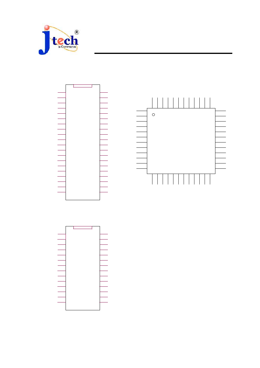
PACKAGE PIN ASSIGNMENT
P04/AIN4
P05/AIN5
P07/AIN7
P40/ADVRF
P20/SEG9
P21/SEG10
P22/RX/SCL/SEG11
P23/TX/SDA/SEG12
P24/SEG13
P25/SEG14
P26/SEG15
P27/SEG16
P36/SEG7
P37/SEG8
P10/PWM0
P11/PWM1
P12/ECT0
P13/VLCD
GND
VDD
P03/AIN3
P02/AIN2
P01/AIN1
P00/AIN0
P35/SEG6
P34/SEG5
P33/SEG4
P32/SEG3
P31/SEG2
P30/SEG1
P41/EXTINT
XIN/ROSC
P42/CLKSEL/TEST
P17/COM4
P16/COM3
P15/COM2
P14/COM1
WT50F6
XOUT
P06/AIN6
/RESET
40 PIN DIP
1
P01/AIN1
P30/SEG1
P16/COM3
VCAP1
P21/SEG10
P20/SEG9
P40/ADVRF
P42/CLKSEL/TEST
P14/COM1
P26/SEG15
VDD
P13/VLCD
P24/SEG13
WT50F6
XOUT
P11/PWM1
P04/AIN4
P37/SEG8
P06/AIN6
NC
1
P32/SEG3
NC
P34/SEG5
NC
P00/AIN0
/RESET
VCAP2
P07/AIN7
P02/AIN2
P15/COM2
P27/SEG16
P03/AIN3
P17/COM4
GND
P25/SEG14
P12/ECT0
P41/EXTIN
XIN/ROSC
P10/PWM0
48 PIN LQFP
P05/AIN5
P36/SEG7
P22/RX/SCL/SEG11
P31/SEG2
NC
P23/TX/SDA/SEG12
P33/SEG4
NC
P35/SEG6
VCAP3
P04/AIN4
P05/AIN5
P07/AIN7
P40/ADVRF
P20/SEG9
P21/SEG10
P22/RX/SCL/SEG11
P23/TX/SDA/SEG12
P24/SEG13
P10/PWM0
P11/PWM1
P12/ECT0
P13/VLCD
GND
VDD
P03/AIN3
P02/AIN2
P01/AIN1
P00/AIN0
P41/EXTINT
XIN/ROSC
P42/CLKSEL/TEST
P16/COM3
P15/COM2
P14/COM1
WT50F6
XOUT
P06/AIN6
/RESET
28 PIN
DIP/SOP(300mil)
1
WT50F6
8-bit
µC with 8KB ISP Flash Memory, 8-CH
12-bit A/D Converter and 16x4 LCD Driver
Preliminary
4 June/12/2001 Ver.1.10
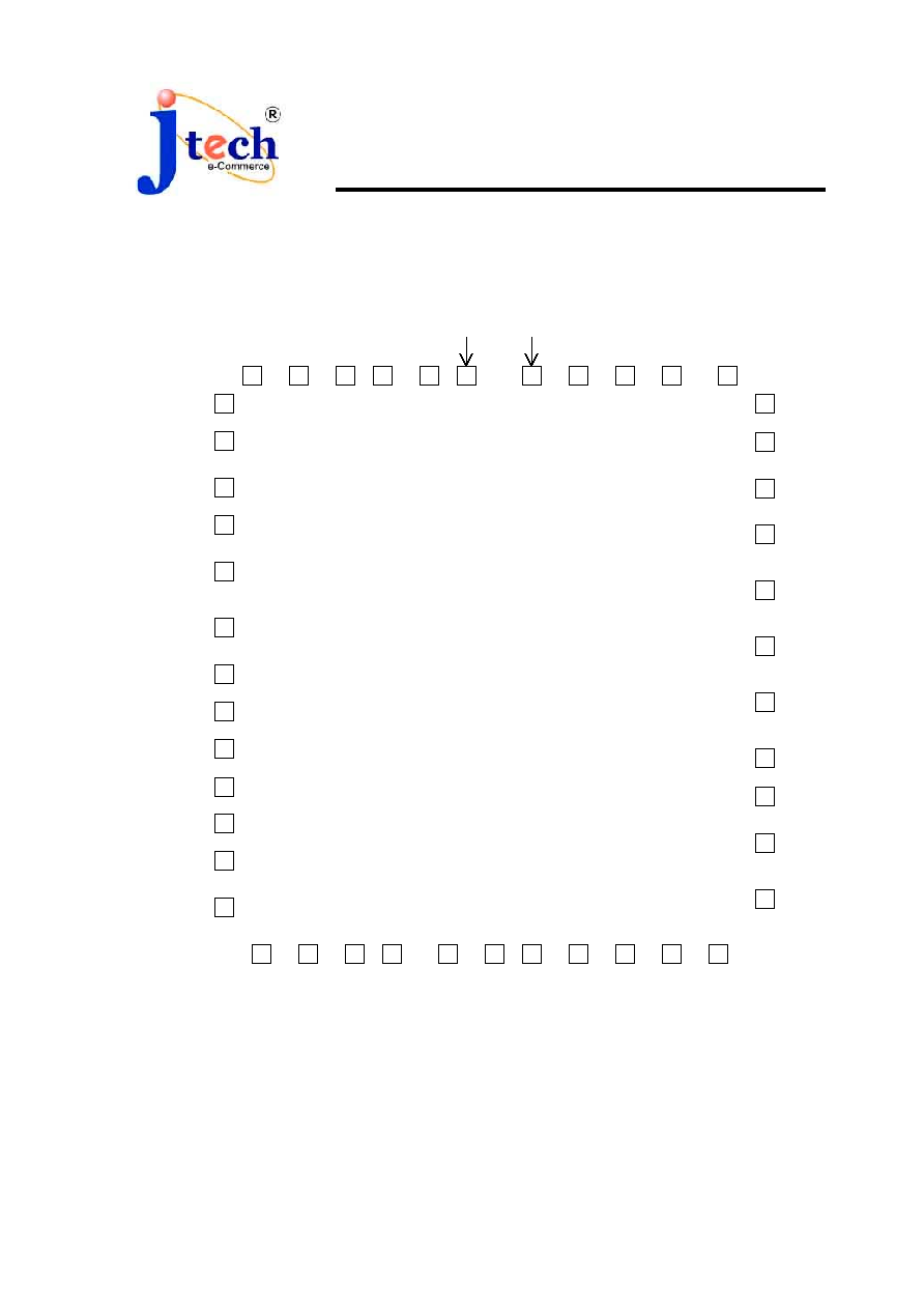
PAD LAYOUT (DIE FORM)
Pin#1
WT50F6
Pin #43
WT50F6
8-bit
µC with 8KB ISP Flash Memory, 8-CH
12-bit A/D Converter and 16x4 LCD Driver
Preliminary
5 June/12/2001 Ver.1.10
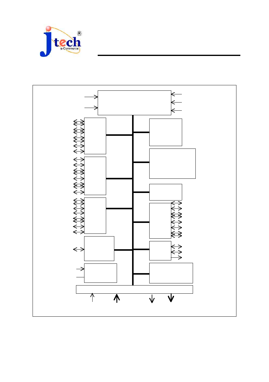
BLOCK DIAGRAM
CPU
RAM
384Byte
Flash Memory
8KBytes
WDT
Dual 16-bit
Timer/Counter 0 &
Timer/Counter 1
P0
P1
P2
Clock
Generator
P00/AIN0
P01/AIN1
P02/AIN2
P03/AIN3
P04/AIN4
P05/AIN5
P06 /AIN6
P07/AIN7
P10/PWM0
P11/PWM1
P12/ECT0
P13/V
LCD
P14/COM1
P15/COM2
P16/COM3
P17/COM4
P20/SEG9
P21/SEG10
P22/RX/SCL/SEG11
P23/TX/SDA/SEG12
P24/SEG13
P25/SEG14
P26/SEG15
P27/ SEG16
VDD
GND
RESET
P42/CLKSEL/TEST
P41/EXTINT
XIN/ROSC
XOUT
8-CH
12-bit
A/D
Converter
P3
P30/SEG1
P31/SEG2
P32/SEG3
P33/SEG4
P34/SEG5
P35/SEG6
P36/SEG7
P37/SEG8
16x4 LCD Driver/Controller
V
LCD
VCAP1/VCAP2/VCAP3 COM1~4 SEG1~16
P4
P40/ADvrf
P41/EXTINT
P42/CLKSEL
P40/ADvrf