1
GENERAL DESCRIPTION
The WT6510 is single chip Micro-controller for Universal Serial Bus (USB) keyboard applications, it with build in pull up
resistors and interrupt capability (8 with high drive capability up to 14mA) implement an USB Keyboard (low speed at
1.5Mhz) with integrated PS/2 port for Pointing Device.
FEATURES
8-bit 6502 CPU with 3MHz operating frequency
6MHz crystal oscillator
256 bytes SRAM
8K bytes MASK ROM
32-36 programmable I/O(Package Dependant) pins with interrupt capability in input mode.
Embedded USB function with three endpoints (one control Enpoint0, two Interrupt IN endpoint)
Watch-dog timer
One 8-bit programmable timer
Low VDD reset
Power on reset
USB Interface (USB Spec. Version 1.1 compliance)
CMOS technology for low power consumption
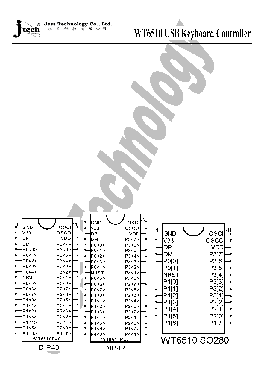
Pin Out

2
PIN DESCRIPTION
Pin No.
40
42
Die
Pin
Name
I/O
Description
1
1
1
GND
P
Ground.
2
2
2
V33
P
3.3V Power output
3
3
3
DP
I/O
USB D+ signal.
4
4
4
DM
I/O
USB D- signal
5
5
5
P00
I/O
General Purpose I/O with programmable pull up resistor and programmable Interrupt
Capability at input falling edge
6
6
6
P01
I/O
General Purpose I/O with programmable pull up resistor and programmable Interrupt
Capability at Input falling edge
7
7
7
P02
I/O
General Purpose I/O with programmable Interrupt Capability at Input falling edge
8
8
8
P03
I/O
General Purpose I/O with programmable Interrupt Capability at Input falling edge
9
9
9
P04
I/O
General Purpose I/O with programmable Interrupt Capability at Input falling edge
10
10
10
NRST
Power on Reset input
11
11
11
P05
I/O
General Purpose I/O with programmable Interrupt Capability at Input falling edge
12
12
12
P06
I/O
General Purpose I/O with programmable Interrupt Capability at Input falling edge
13
13
13
P07
I/O
General Purpose I/O with programmable Interrupt Capability at Input falling edge
14
14
14
P10
I/O
General Purpose FO with programmable Interrupt Capability at Input falling edge
15
15
15
P11
I/O
General Purpose I/O with programmable Interrupt Capability at Input falling edge
16
16
16
P12
I/O
General Purpose I/O with programmable Interrupt Capability at Input falling edge
17
17
17
P13
I/O
General Purpose I/O with programmable Interrupt Capability at Input falling edge
18
18
18
P14
I/O
General Purpose I/O with programmable Interrupt Capability at Input falling edge
19
19
19
P15
I/O
General Purpose I/O with programmable Interrupt Capability at Input falling edge
20
20
20
P16
I/O
General Purpose I/O with programmable Interrupt Capability at Input falling edge
21
21
P40
I/O
General Purpose I/O with programmable Interrupt Capability at Input falling edge
22
22
P41
I/O
General Purpose I/O with programmable Interrupt Capability at Input falling edge
23
P42
I/O
General Purpose I/O with programmable Interrupt Capability at Input falling edge
24
P43
I/O
General Purpose I/O with programmable Interrupt Capability at Input falling edge
21
23
25
P17
I/O
General Purpose I/O with programmable Interrupt Capability at Input falling edge
22
24
26
P20
I/O
General Purpose I/O with programmable Interrupt Capability at Input falling edge
23
25
27
P21
I/O
General Purpose I/O with programmable Interrupt Capability at Input falling edge
24
26
28
P22
I/O
General Purpose I/O with programmable Interrupt Capability at Input falling edge
25
27
29
P23
I/O
General Purpose I/O with programmable Interrupt Capability at Input falling edge
26
28
30
P24
I/O
General Purpose I/O with programmable Interrupt Capability at Input falling edge
27
29
31
P25
I/O
General Purpose I/O with programmable Interrupt Capability at Input falling edge
28
30
32
P26
I/O
General Purpose I/O with programmable Interrupt Capability at Input falling edge
29
31
33
P27
I/O
General Purpose I/O with programmable Interrupt Capability at Input falling edge
30
32
34
P30
I/O
General Purpose I/O with programmable Interrupt Capability at Input falling edge
High current drive with typical current sink capability of 14mA
31
33
35
P31
I/O
General Purpose I/O with programmable Interrupt Capability at Input falling edge
High current drive with typical current sink capability of 14mA
32
34
36
P32
I/O
General Purpose I/O with programmable Interrupt Capability at Input falling edge
High current drive with typical current sink capability of 14mA
33
35
37
P33
I/O
General Purpose I/O with programmable Interrupt Capability at Input falling edge
High current drive with typical current sink capability of 14mA
34
36
38
P34
I/O
General Purpose I/O with programmable Interrupt Capability at Input falling edge
High current drive with typical current sink capability of 14mA
35
37
39
P35
I/O
General Purpose I/O with programmable Interrupt Capability at Input falling edge
High current drive with typical current sink capability of 14mA
36
38
40
P36
I/O
General Purpose I/O with programmable Interrupt Capability at Input falling edge
High current drive with typical current sink capability of 14mA
37
39
41
P37
I/O
General Purpose I/O with programmable Interrupt Capability at Input falling edge
High current drive with typical current sink capability of 14mA
38
40
42
VDD
P
+5V power supply.
39
41
43
OSCO
O
6MHz oscillator output.
40
42
44
OSCI
I
6MHz oscillator input.

3
WT6510 Register mapping
Name
Addr R/W Initial
Bit7
Bit6
Bit5
Bit4
Bit3
Bit2
Bit1
Bit0
P0_CTRL
00h
W
00h
P07OE
P06OE
P05OE
P04OE
P03OE
P02OE
P01OE
P00OE
R
00h
P07
P06
P05
P04
P03
P02
P01
P00
P0_DATA
01h
W
00h
P07
P06
P05
P04
P03
P02
P01
P00
P1_CTRL
02h
W
00h
P17OE
P16OE
P15OE
P14OE
P13OE
P12OE
P11OE
P10OE
R
00h
P17
P16
P15
P14
P13
P12
P11
P10
P1_DATA
03h
W
00h
P17
P16
P15
P14
P13
P12
P11
P10
P2_CTRL
04h
W
00h
P27OE
P26OE
P25OE
P24OE
P23OE
P22OE
P21OE
P20OE
R
00h
P27
P26
P25
P24
P23
P22
P21
P20
P2_DATA
05h
W
00h
P27
P26
P25
P24
P23
P22
P21
P20
P3_CTRL
06h
W
00h
P37OE
P36OE
P35OE
P34OE
P33OE
P32OE
P31OE
P30OE
R
00h
P37
P36
P35
P34
P33
P32
P31
P30
P3_DATA
07h
W
00h
P37
P36
P35
P34
P33
P32
P31
P30
P4_CTRL
08h
W
00h
--
--
--
--
P43OE
P42OE
P41OE
P40OE
R
00h
--
--
--
--
P43
P42
P41
P40
P4_DATA
09h
W
00h
--
--
--
--
P43
P42
P41
P40
TIMER
10h
W
00h
PS1
PS0
TIM5
TIM4
TIM3
TIM2
TIM1
TIM0
INT_FLAG 11h
R
00h
--
--
--
--
--
IF_IOINT IF_USB
IF_TMR
INT_EN
11h
W
00h
IE_P4INT CR_IOINT IE_P3INT IE_P2INT IEP1INT IE_P0INT IE_USB
IE_TMR
WDT
12h
W
00h
--
--
--
--
--
--
--
--
DISWDT
17h
W
00h
--
--
--
--
--
--
--
DISWDT
PWRMGE 13h
W
00h
--
--
--
--
--
--
RESUME SUSPEND
USB_ADR 20h
W
00h
EN_USB
UADR6
UADR5
UADR4
UADR3
UADR2
UADR1
UADR0
USB_ICR
21h
W
00h
--
IE_RSMI EN_EP2INEN_EP1INEN_EP0IN EN_RST EN_OUT EN_SET
USB_EVENT
21h
R
00h
ACTIVE IF_RSMI
EP2IN
EP1IN
EP0IN
RESET
OUT
SETUP
USB_FIFO0 22h
R/W XXh
F0_D7
F0_D6
F0_D5
F0_D4
F0_D3
F0_D2
F0_D1
F0_D0
USB_CNT 23h
R
--
UNDERN TX_OVF RXEMP
UCNT3
UCNT2
UCNT1
UCNT0
USB_CLR 23h
W
00h
CLR_ACT CLR_INT CLR_UC0 CLR_UC0 CLR_DC1 CLR_DC1 CLR_UC2 CLR_UC2
USB_CR0
24h
W
00h
--
--
--
OUT_STL EN_OUT
EP0_IN_STL EP0_VALID
EP0_PAK
USB_ST0
24h
R
00h
DATA0/1
OUT_STL OUT_OK
EP0_STALL
EP0_FAIL EP0_OK
USB_FIFO1 25h
W
XXh
F1_D7
F1_D6
F1_D5
F1_D4
F1_D3
F1_D2
F1_D1
F1_D0
USB_CR1
26h
W
00h
--
--
--
--
EN_EP1 IN1_STL EP1_VAL EP1_PAK
USB_ST1
26h
R
00h
--
--
--
--
--
EP1_STALL
EP1_FAIL EP1_OK
USB_FIFO2 27
W
XXh
F2_D7
F2_D6
F2_D5
F2_D4
F2_D3
F2_D2
F2_D1
F2_D0
USB_CR2
28h
W
00h
--
--
--
--
EN_EP2 IN2_STL EP2_VAL EP2_PAK
USB_ST2
28h
R
00h
--
--
--
--
--
EP2_STALL
EP2_FAIL EP2_OK

4
FUNCTIONAL DESCRIPTION
CPU
8-bit 6502 compatible CPU operates at 3MHz. Address bus is 16-bit and data bus is 8-bit. The non-maskable interrupt (/NMI)
of 6502 is modified to be maskable and is defined as INT0 (IF_IOINT) with higher priority. The interrupt request (/IRQ) of
6502 is defined as INT1 (IF_TMR & IF_USB) with lower priority.
Default stack pointer is $01FFh.
Please refer the 6502 reference menu for more detail.
RAM
256 bytes RAM. Address is located From $0080h to $00FFh; $0180h to $01FFh
MASK ROM
8K Bytes MASK ROM
The following addresses are reserved for special purpose:
$FFFAh (Iow byte) and $FFFBh (high byte): INT0 interrupt vector.
$FFFCh (Iow byte) and $FFFDh (high byte): program reset interrupt vector
$FFFEh (Iow byte) and $FFFFh (high byte): INT1 interrupt vector.
Oscillator
6MHz crystal oscillator. Feedback resistor is built in.
It can be turned off by setting a control bit and wake up by I/O port or resume USB Host.
3.3V Regulator
A built-in 3.3V regulator supply power for USB transceiver.
External capacitor is required. Can supply over 35mA.
5
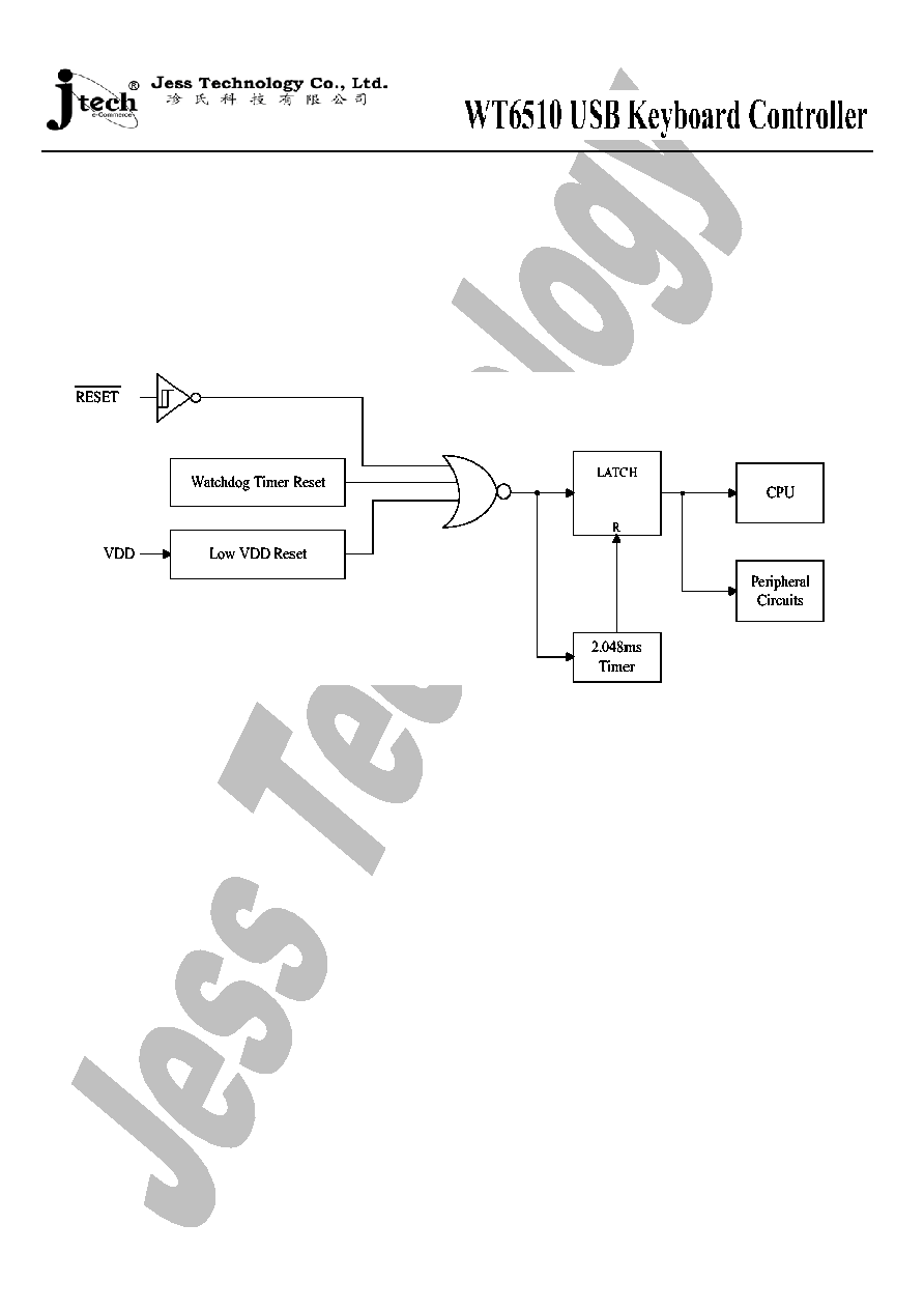
System Reset
There are four reset sources of this controller. Fig.1 shows the block diagram of reset logic.
Fig. 1 Reset Signals
External Reset
A low level on the/ RESET(NRST) pin will generate reset.
Low VDD Voltage Reset
When VDD is below 3.7V (typical), an internal reset signal will last 2.048ms after the voltage is higher than 3.7V (typical)
Watchdog Timer Reset
If a time-out happens when watchdog timer is enabled, a reset pulse is generated. Please refer watchdog timer section for
more information.
General Purpose I/O Ports
Ports 0 to 2 provide 24 general purpose I/O pins that can be read or written. Each port (8 bits) can be configured as inputs
with internal pull-ups, or traditional CMOS outputs. Ports 0 to 2 are considered low current drive with typical current sink
capability of 10mA. The internal pull-up resistors are typically 25 Kohms.

6
Port 3 has eight general purpose I/O pins. Port 3 (8-bits) can be configured as inputs with internal pull-ups, or traditional
CMOS outputs. Port 3 offers high current drive with a typical current sink capability of 20mA. The internal pull-up resistors
are typically 25 Kohms. After reset, all of the GPIO pins are set to input with the internal pull-up enabled.
Every GPIO port can be programmed as inputs with internal pull-ups, and traditional CMOS outputs. In addition, an input pin
causes an interrupt (if it is interrupt enabled) with negative polarity ( a falling edge ).
** P00, P01 might initialize as input without pull-up resistor. Only when the P0_CTRL=0 and P0_DATA=1, these pin(s)
might set as input and with internal pull-up resistor.
P0_CTRL: Port0 Direction Register
Name
Addr
R/W
Initial
Bit7
Bit6
Bit5
Bit4
Bit3
Bit2
Bit1
Bit0
P0_CTRL
00H
W
00H
P07OE
P06OE
P05OE
P04OE
P03OE
P02OE
P01OE
P00OE
P0_CTRL: Indicate Port0 direction.
P0nOE: =1: means output enable.
P0_DATA: Port0 Data Register
Name
Addr
R/W
Initial
Bit7
Bit6
Bit5
Bit4
Bit3
Bit2
Bit1
Bit0
R
P0_DATA
01H
W
00H
P07
P06
P05
P04
P03
P02
P01
P00
P0_DATA register shows the data read or write to Port0 [7:0]
P0n: =1: data read or write to Port0 [n] is 1
=0: data read or write to Port0 [n] is 0
P1_CTRL: Port1 Direction Register
Name
Addr
R/W
Initial
Bit7
Bit6
Bit5
Bit4
Bit3
Bit2
Bit1
Bit0
P1_CTRL
02H
W
00H
P17OE
P16OE
P15OE
P14OE
P13OE
P12OE
P11OE
P10OE
P1_CTRL: Indicate Port1 direction.
P1nOE: =1: means output enable.
P1_DATA: Port1 Data Register
Name
Addr
R/W
Initial
Bit7
Bit6
Bit5
Bit4
Bit3
Bit2
Bit1
Bit0
R
00H
P17
P16
P05
P14
P13
P12
P11
P10
P1_DATA
03H
W
00H
P17
P16
P15
P14
P13
P12
P11
P10
P1_DATA register shows the data read to write to Port1 [7:0]
P1n: =1: data read or write to Port [n] is 1
=0: data read or write to Port [n] is 0
P2_CTRL: Port2 Direction Register
Name
Addr
R/W
Initial
Bit7
Bit6
Bit5
Bit4
Bit3
Bit2
Bit1
Bit0
P2_CTRL
04H
W
00H
P27OE
P26OE
P25OE
P24OE
P23OE
P22OE
P21OE
P20OE
P2_CTRL: Indicate Port2 direction.
P2nOE: =1 means output enable.
7
P2_DATA: Port2 Direction Register
Name
Addr
R/W
Initial
Bit7
Bit6
Bit5
Bit4
Bit3
Bit2
Bit1
Bit0
R
00H
P27
P26
P25
P24
P23
P22
P21
P20
P2_DATA
05H
W
00H
P27
P26
P25
P24
P23
P22
P21
P20
P2_DATA register shows the data read to write to Port2 [7:0]
P2n: =1: data read or write to Port2 [n] is 1
=0: data read or write to Port2 [n] is 0
P3_CTRL: Port3 Direction Register
Name
Addr
R/W
Initial
Bit7
Bit6
Bit5
Bit4
Bit3
Bit2
Bit1
Bit0
P3_CTRL
06H
W
00H
P37OE
P36OE
P35OE
P34OE
P33OE
P32OE
P31OE
P30OE
P3_CTRL: Indicate Port3 direction.
P3nOE: =1 means output enable.
P3_DATA: Port3 Direction Register
Name
Addr
R/W
Initial
Bit7
Bit6
Bit5
Bit4
Bit3
Bit2
Bit1
Bit0
R
00H
P37
P36
P35
P34
P33
P32
P31
P30
P3_DATA
07H
W
00H
P37
P36
P35
P34
P33
P32
P31
P30
P3_DATA register shows the data read to write to Port3 [7:0]
P3n: =1: data read or write to Port 3 [n] is 1
=0: data read or write to Port 3 [n] is 0
P4_CTRL: Port4 Direction Register
Name
Addr
R/W
Initial
Bit7
Bit6
Bit5
Bit4
Bit3
Bit2
Bit1
Bit0
P4_CTRL
08H
W
00H
--
--
--
--
P43OE
P42OE
P41OE
P40OE
P4_CTRL: Indicate Port4 direction.
P4nOE: =1 means output enable.
P4_DATA: Port4 Direction Register
Name
Addr
R/W
Initial
Bit7
Bit6
Bit5
Bit4
Bit3
Bit2
Bit1
Bit0
R
00H
--
--
--
--
P43
P42
P41
P40
P4_DATA
09H
W
00H
--
--
--
--
P43
P42
P41
P40
P4_DATA register shows the data read to write to Port4 [7:0]
P4n: =1: data read or write to Port 4 [n] is 1
=0: data read or write to Port 4 [n] is 0
Timer
It is a 6-bit down counter with 2-bit prescaler. The time base is selected by PS1 and PS0 bits. Timer starts counting when
writing data to TIMER register. When the counter counts to zero, the counter stops and set interrupt flag IF_TMR. If user
wants to start the timer again to TIMER register.
Name
Addr
R/W
Initial
Bit7
Bit6
Bit5
Bit4
Bit3
Bit2
Bit1
Bit0
TIMER
10H
W
00H
PS1
PS0
TIM5
TIM4
TIM3
TIM2
TIM1
TIM0
Bit Name
Bit Description
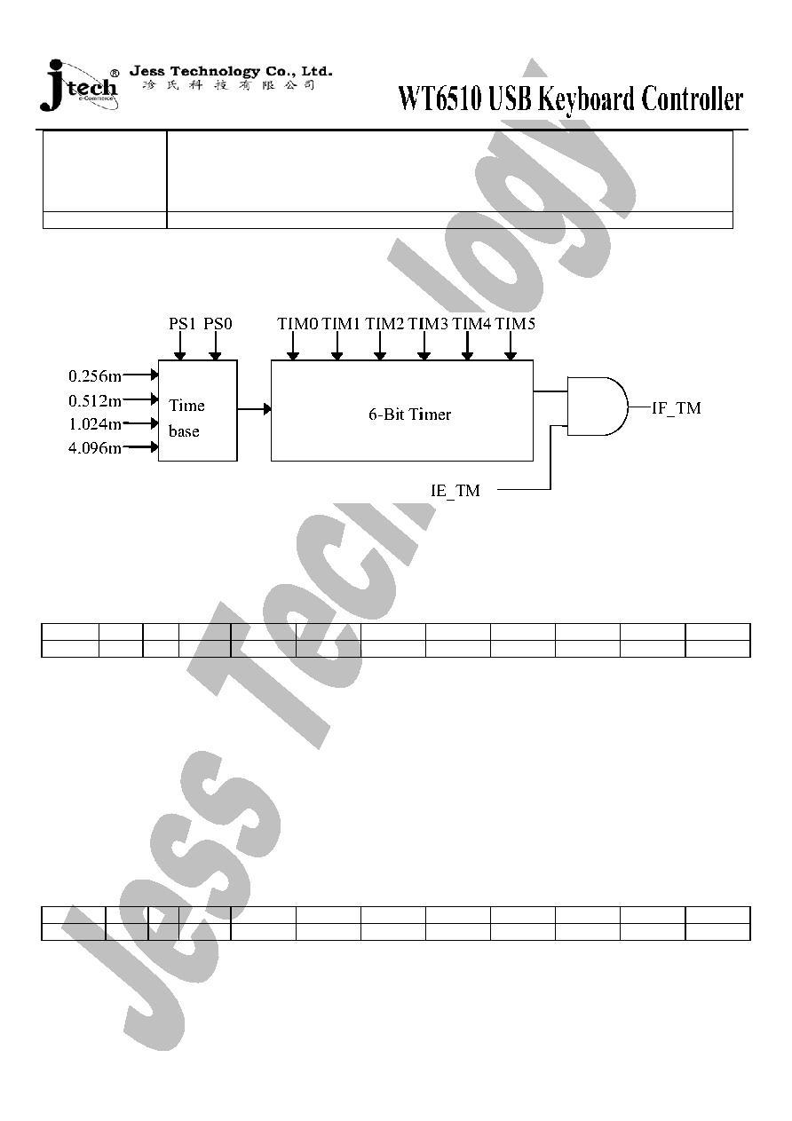
8
PS1, PS0
Prescaler of timer.
"00": time base = 0.256ms
"01": time base = 0.512ms
"10": time base = 1.024ms
"11": time base = 4.096ms
TIM5 ~ TIM0
Timer period = time base x (6-bit data)
Interrupt control
NMI: I/O port wake up. Falling edge trigger.
IRQ: USB Event, Timer
INT-EN: Enable interrupt source Register
Name
Addr
R/W Initial
Bit7
Bit6
Bit5
Bit4
Bit3
Bit2
Bit1
Bit0
INT-EN 11H
W
00H
IE_P4INT CR_IOINT IE_P3INT IE_P2INT IE_P1INT IE_P0INT IE_USB
IE_TMR
INT-EN: Enable interrupt source register
IE_TMR: =1: Enable timer interrupt source.
=0: Disable timer interrupt source.
IE_USB: =1: Enable USB event interrupt source, please refer to USB_ISR register
=0: Disable USB event interrupt source.
IE_PnINT: =1: Enable Port(n) I/O port interrupt source.
=0: Disable port(n) I/O port interrupt source.
CR_IOINT: =1: Clear I/O interrupt event.
PS: Clear timer interrupt flag by re-write a new data to timer register.
Clear USB interrupt flag by write CLR_INT of Reg23H.
INT FLAG: Interrupt Flag register
Name
Addr R/W Initial
Bit7
Bit6
Bit5
Bit4
Bit3
Bit2
Bit1
Bit0
INT_FLAG
11H
R
00H
--
--
--
--
--
IF_IOINT
IF_USB
IF_TMR
INT_FLAG Register Indicates which interrupt event occurs.
IF_TMR: =1: Timer interrupt occur.
IF_USB: =1: USB event occur. ( refer to USB_ISR)
IF_IOINT: =1: Any I/O pins detect interrupt occurs.

9
Watchdog Timer
Watchdog timer will generate a reset pulse if CPU does not write WDT register within 259.072ms or 518.144ms. This
function can be disable by cleared ENWDT bit.
Name
Addr R/W Initial
Bit7
Bit6
Bit5
Bit4
Bit3
Bit2
Bit1
Bit0
DISWDT
17H
W
X0H
--
--
--
--
--
--
--
DISWDT
Bit Name
Bit Value = "1"
Bit value = "0"
DISWDT
Disable Watch Dog Timer
Enable Watch Dog Timer
USB Interface
The USB interface contains three endpoints : Control endpoint 0, Interrupt IN endpoint 1 and endpoint2. Endpoint 0 has IN
FIFO (transmit) and OUT FIFO (receive). Endpoint 1 and Endpoint2 have IN FIFO only. All FIFOs are 8 bytes.
PWRMGE: USB Power-management Register
Name
Addr R/W Initial
Bit7
Bit6
Bit5
Bit4
Bit3
Bit2
Bit1
Bit0
PWRMGE 13H
W
00H
--
--
--
--
--
--
RESUME
SUSPEND
Resume: =1: Send resume signal on the USB bus toward to Host as remote wake-up
Suspend: =1: Force the USB device into the suspend ( power down ) mode.
10
USB_ADR: USB device address and Enable
Name
Addr R/W Initial
Bit7
Bit6
Bit5
Bit4
Bit3
Bit2
Bit1
Bit0
USB_ADR 20H
W
00h
EN_USB UADR6 UADR5 UADR4 UADR3
UADR2
UADR1
UADR0
USB ADR: Enable the USB function and write the device address (Host set.).
EN_USB: =1: Enable USB Function(turn on pull-up resistor in DM pin)
UADR[6:0]: The USB Device address set by Host
USB_ICR: Enable USB event interrupt source Register.
Name
Addr R/W Initial
Bit7
Bit6
Bit5
Bit4
Bit3
Bit2
Bit1
Bit0
USB_ICR 21h
W
00h
--
E_RESUM EN_EP2IN EN_EP1IN EN_EP0IN EN_RST
EN_OUT
EN_SET
USB_ICR: Enable USB event interrupt source register
E_RESUM: =1: Enable Resume_IN event interupt.
EN_EP2IN: =1: Enable EndPoint2 IN_Token transaction event interrupt
EN_EP1IN: =1: Enable EndPoint1 IN_Token transaction event interrupt
EN_EP0IN: =1: Enable EndPoint0 IN_Token transaction event interrupt
EN_RST: =1: Enable USB_Reset transaction event interrupt.
EN_OUT: =1: Enable EndPoint0 OUT_Token transaction event interrupt.
EN_SET: =1: Enable EndPoint0 Setup_Token transaction event interrupt.
USB_EVENT: USB event register
Name
Addr R/W Initial
Bit7
Bit6
Bit5
Bit4
Bit3
Bit2
Bit1
Bit0
USB_EVENT 21h
R
00h
ACTIVE IF_RSM
EP2IN
EPIIN
EPOIN
RESET
OUT
SETUP
USB EVENT: Indicate USB event occur.
Active: =1 USB bus keep alive. ( non_idle )
IF_RSMI: =1 Resume signal in (received)
EP0/I/21N: =1 EndPoint0/l/2 IN_Token transaction occur(O.K., fail or Stall. Refence USB_ST0/I/2).
Reset: =1 USB reset event occur.
OUT: =1 EndPoint0 OUT_Token transaction occur(O.K, or Stall. Refence USB_ST0)
SETUP: -1 EndPoint0 Setup_Token transaction occur(O.K, only).
USB_FIFO0: EndPoint0 FIFO
Name
Addr
R/W Initial
Bit7
Bit6
Bit5
Bit4
Bit3
Bit2
Bit1
Bit0
USB_FIFO0
22H
R/W
XXH
F0_D7
F0_D6
F0_D5
F0_D4
F0_D3
F0_D2
F0_D1
F0_D0
USB_FIFO0: Read/Write data / to EndPoint0 FIFO
F0_Dn: Data Read/Write / to Endpoint0 FIFO
USB_CNT: USB FIFO Counter and Status Register
Name
Addr
R/W Initial
Bit7
Bit6
Bit5
Bit4
Bit3
Bit2
Bit1
Bit0
USB_CNT
23H
R
--
UNDERN TX_OVF RXEMP UCNT3 UCNT2
UCNT1
UCNT0
USB_CNT: USB FIFO Counter and Status Register
UNDERN: =1 Host Counter under-run.
TX_OVF: =1 FIFO0 over-flow
RXEM: =1 Indicate the Host counter is empty
UCNT [3-0]: Endpoint0 FIFO Host counter.

11
USB_CLR: USB Clear Register
Name
Addr
R/W Initial
Bit7
Bit6
Bit5
Bit4
Bit3
Bit2
Bit1
Bit0
USB_CLR
23H
W
00H
CLR_ACT CLR_INT CLR_UC0 CLR_DC0 CLR_UC1 CLR_DC1 CLR_UC2 CLR_DC2
CLR_ACT: =1 Clear the active bit.
CLR_INT: =1 Clear the USB interrupt event(all flags).
CLR_UC0/1/2: =1 Clear the EndPoint0/1/2 Host counter.
CLR_UD0/1/2: =1 Clear the Endpoint0/1//2 Device counter.
USB_CR0:
Name
Addr
R/W Initial
Bit7
Bit6
Bit5
Bit4
Bit3
Bit2
Bit1
Bit0
USB_CR0
24H
W
00H
--
--
--
OUT_STL
EN_OUT
EP0_IN_STL EP0_VALID
EP0_PAK
USB_CR0:
OUT_STL: =1 Send Stall token at the next Out transaction
EN_OUT: =1 Enable Endpoint0 OUT pipe.
EP0_IN_STL: =1 FIFO0 data valid to send at the next Endpoint0 IN transaction.
EP0_PAK: =1 Indicate the Data packet will send at the next Endpoint0 IN transaction.
USB_ST0: Endpoint0 Status register
Name
Addr
R/W Initial
Bit7
Bit6 Bit5
Bit4
Bit3
Bit2
Bit1
Bit0
USB_ST0
24H
R
00H
DATA0/1
OUT_STL
OUT_OK
EP0_Stall
EP0_Fail
EP0_OK
DATA0/1: =1 Indicate the previous Setup/Out token Data packet.
OUT_STL: =1 Indicate the previous Out transaction Stall.
OUT_OK: =1 Indicate the previous Out transaction complete.
EP0_Stall: =1 Indicate the previous Endpoint0 IN transaction Stall.
EP0_Fail: =1 Indicate the previous Edpoint0 IN transaction fail. (lose hand-shack)
EP0_OK: =1 Indicate the previous Endpoint0 IN transaction complete.
USB_FIFO1: EndPoint1 FIFO.
Name
Addr
R/W Initial
Bit7
Bit6
Bit5
Bit4
Bit3
Bit2
Bit1
Bit0
USB_FIFO1
25H
W
XXH
F1_D7
F1_D6
F1_D5
F1_D4
F1_D3
F1_D2
F1_D1
F1_D0
USB_FIFO1: Write data to EndPoint1 FIFO.
F1_Dn: Data Read/Write/ to EndPoint1 FIFO.
USB_CR1: EndPont1 Control Register
Name
Addr
R/W Initial
Bit7
Bit6
Bit5
Bit4
Bit3
Bit2
Bit1
Bit0
USB_CR1
26H
W
00H
--
--
--
--
EN_EP1
IN1_STL
EP1_VAL EP1_PAK
EP1_STL: =1 Send Stall token at the next EndPoint1 IN transaction.
EP1_VAL: =1 FIFO1 data valid to send at the next EndPoint1 IN transaction.
EP1/2_PAK: =1 Indicate the Data packet will send at the next EndPoint1/2 IN transaction.
USB_ST1: EndPoint1 Status Register
Name
Addr
R/W Initial
Bit7
Bit6
Bit5
Bit4
Bit3
Bit2
Bit1
Bit0
USB_ST1
26H
R
00H
--
--
--
--
--
EP1_Stall
EP1_Fail
EP1_OK
EP1_Stall: =1 Indicate the previous EndPoint1 IN transaction Stall.
EP1_Fail: =1 Indicate the previous EndPoint1 IN transaction fail. (lose hand-shack)

12
EP1_OK: =1 Indicate the previous EndPoint1 In transaction complete.
USB_FIFO2: EndPoint2 FIFO.
Name
Addr
R/W Initial
Bit7
Bit6
Bit5
Bit4
Bit3
Bit2
Bit1
Bit0
USB_FIFO2
27H
W
XXH
F2_D7
F2_D6
F2_D5
F2_D4
F2_D3
F2_D2
F2_D1
F2_D0
F2_Dn: Data read/Write data from/to Endpoint2 FIFO
USB_CR2: EndPont1 Control Register
Name
Addr
R/W Initial
Bit7
Bit6
Bit5
Bit4
Bit3
Bit2
Bit1
Bit0
USB_CR2
28H
W
00H
--
--
--
--
EN_EP2
IN2_STL
EP2_VAL EP2_PAK
EP2_STL: =1 Send Stall token at the next EndPoint2 IN transaction.
EP2_VAL: =1 FIFO2 data valid to send at the next EndPoint2 IN transaction.
EP2_PAK: =1 Indicate the Data packet will send at the next EndPoint2 IN transaction.
USB_ST2: EndPoint1 Status Register
Name
Addr
R/W Initial
Bit7
Bit6
Bit5
Bit4
Bit3
Bit2
Bit1
Bit0
USB_ST2
28H
R
00H
--
--
--
--
--
EP2_Stall
EP2_Fail
EP2_OK
EP2_Stall: =1 Indicate the previous EndPoint2 IN transaction Stall.
EP2_Fail: =1 Indicate the previous EndPoint2 IN transaction fail. (lose hand-shack)
EP2_OK: =1 Indicate the previous EndPoint2 In transaction complete.
ELECTRICAL CHARACTERISTICS
Absolute Maximum Ratings
Parameter
Min.
Max.
Unites
DC Supply Voltage (VDD)
-0.3
7.0
V
Input and output voltage with respect to Ground
-0.3
VDD+0.3
V
Storage temperature
-25
125
Ambient temperature with power applied
0
85
* Note: Stresses above those listed may cause permanent damage to the devices
D.C Characteristics (VDD=5.0V�5%, Ta=0-70)
Symbol
Parameter
Condition
Min.
Typ.
Max.
Units
V
DD
Supply Voltage
4.0
5
5.5
V
V
IH
Input High Voltage
0.7V
DD
--
V
DD
+0.3
V
V
IL
Input Low Voltage
-0.3
--
0.3V
DD
V
V
OH
Output High Voltage
I
OH
= -8mA
4
V
DD
V
V
OL
Output Low Voltage
I
OL
= 8mA
0
0.4
V
Isink2
Sink Current for Port3
14
20
mA
I
IL
Input Leakage Current
0V < V
IN
<V
DD
-1
--
1
A
R
PH
Pull High Resistance
25
Kohm
I
DD.OPT
Operating Current
F
OSC
=6MHz, No load
10
mA
I
DD.SBY
Standby current
Oscillator disabled. No Load
300
A
V33
3.3V regulator output
3.2
3.3
3.4
V
V
RESET
Reset Voltage
3.6
3.7
3.8
V