2
PIN DESCRIPTION
Pin No.
40
42
Die
Pin
Name
I/O
Description
1
1
1
GND
P
Ground.
2
2
2
V33
P
3.3V Power output
3
3
3
DP
I/O
USB D+ signal.
4
4
4
DM
I/O
USB D- signal
5
5
5
P00
I/O
General Purpose I/O with programmable pull up resistor and programmable Interrupt
Capability at input falling edge
6
6
6
P01
I/O
General Purpose I/O with programmable pull up resistor and programmable Interrupt
Capability at Input falling edge
7
7
7
P02
I/O
General Purpose I/O with programmable Interrupt Capability at Input falling edge
8
8
8
P03
I/O
General Purpose I/O with programmable Interrupt Capability at Input falling edge
9
9
9
P04
I/O
General Purpose I/O with programmable Interrupt Capability at Input falling edge
10
10
10
NRST
Power on Reset input
11
11
11
P05
I/O
General Purpose I/O with programmable Interrupt Capability at Input falling edge
12
12
12
P06
I/O
General Purpose I/O with programmable Interrupt Capability at Input falling edge
13
13
13
P07
I/O
General Purpose I/O with programmable Interrupt Capability at Input falling edge
14
14
14
P10
I/O
General Purpose FO with programmable Interrupt Capability at Input falling edge
15
15
15
P11
I/O
General Purpose I/O with programmable Interrupt Capability at Input falling edge
16
16
16
P12
I/O
General Purpose I/O with programmable Interrupt Capability at Input falling edge
17
17
17
P13
I/O
General Purpose I/O with programmable Interrupt Capability at Input falling edge
18
18
18
P14
I/O
General Purpose I/O with programmable Interrupt Capability at Input falling edge
19
19
19
P15
I/O
General Purpose I/O with programmable Interrupt Capability at Input falling edge
20
20
20
P16
I/O
General Purpose I/O with programmable Interrupt Capability at Input falling edge
21
21
P40
I/O
General Purpose I/O with programmable Interrupt Capability at Input falling edge
22
22
P41
I/O
General Purpose I/O with programmable Interrupt Capability at Input falling edge
23
P42
I/O
General Purpose I/O with programmable Interrupt Capability at Input falling edge
24
P43
I/O
General Purpose I/O with programmable Interrupt Capability at Input falling edge
21
23
25
P17
I/O
General Purpose I/O with programmable Interrupt Capability at Input falling edge
22
24
26
P20
I/O
General Purpose I/O with programmable Interrupt Capability at Input falling edge
23
25
27
P21
I/O
General Purpose I/O with programmable Interrupt Capability at Input falling edge
24
26
28
P22
I/O
General Purpose I/O with programmable Interrupt Capability at Input falling edge
25
27
29
P23
I/O
General Purpose I/O with programmable Interrupt Capability at Input falling edge
26
28
30
P24
I/O
General Purpose I/O with programmable Interrupt Capability at Input falling edge
27
29
31
P25
I/O
General Purpose I/O with programmable Interrupt Capability at Input falling edge
28
30
32
P26
I/O
General Purpose I/O with programmable Interrupt Capability at Input falling edge
29
31
33
P27
I/O
General Purpose I/O with programmable Interrupt Capability at Input falling edge
30
32
34
P30
I/O
General Purpose I/O with programmable Interrupt Capability at Input falling edge
High current drive with typical current sink capability of 14mA
31
33
35
P31
I/O
General Purpose I/O with programmable Interrupt Capability at Input falling edge
High current drive with typical current sink capability of 14mA
32
34
36
P32
I/O
General Purpose I/O with programmable Interrupt Capability at Input falling edge
High current drive with typical current sink capability of 14mA
33
35
37
P33
I/O
General Purpose I/O with programmable Interrupt Capability at Input falling edge
High current drive with typical current sink capability of 14mA
34
36
38
P34
I/O
General Purpose I/O with programmable Interrupt Capability at Input falling edge
High current drive with typical current sink capability of 14mA
35
37
39
P35
I/O
General Purpose I/O with programmable Interrupt Capability at Input falling edge
High current drive with typical current sink capability of 14mA
36
38
40
P36
I/O
General Purpose I/O with programmable Interrupt Capability at Input falling edge
High current drive with typical current sink capability of 14mA
37
39
41
P37
I/O
General Purpose I/O with programmable Interrupt Capability at Input falling edge
High current drive with typical current sink capability of 14mA
38
40
42
VDD
P
+5V power supply.
39
41
43
OSCO
O
6MHz oscillator output.
40
42
44
OSCI
I
6MHz oscillator input.
3
WT65F1 Register mapping
Name
Addr R/W Initial
Bit7
Bit6
Bit5
Bit4
Bit3
Bit2
Bit1
Bit0
P0_CTRL
00h
W
00h
P07OE
P06OE
P05OE
P04OE
P03OE
P02OE
P01OE
P00OE
R
00h
P07
P06
P05
P04
P03
P02
P01
P00
P0_DATA
01h
W
00h
P07
P06
P05
P04
P03
P02
P01
P00
P1_CTRL
02h
W
00h
P17OE
P16OE
P15OE
P14OE
P13OE
P12OE
P11OE
P10OE
R
00h
P17
P16
P15
P14
P13
P12
P11
P10
P1_DATA
03h
W
00h
P17
P16
P15
P14
P13
P12
P11
P10
P2_CTRL
04h
W
00h
P27OE
P26OE
P25OE
P24OE
P23OE
P22OE
P21OE
P20OE
R
00h
P27
P26
P25
P24
P23
P22
P21
P20
P2_DATA
05h
W
00h
P27
P26
P25
P24
P23
P22
P21
P20
P3_CTRL
06h
W
00h
P37OE
P36OE
P35OE
P34OE
P33OE
P32OE
P31OE
P30OE
R
00h
P37
P36
P35
P34
P33
P32
P31
P30
P3_DATA
07h
W
00h
P37
P36
P35
P34
P33
P32
P31
P30
P4_CTRL
08h
W
00h
--
--
--
--
P43OE
P42OE
P41OE
P40OE
R
00h
--
--
--
--
P43
P42
P41
P40
P4_DATA
09h
W
00h
--
--
--
--
P43
P42
P41
P40
TIMER
10h
W
00h
PS1
PS0
TIM5
TIM4
TIM3
TIM2
TIM1
TIM0
INT_FLAG 11h
R
00h
--
--
--
--
--
IF_IOINT IF_USB
IF_TMR
INT_EN
11h
W
00h
IE_P4INT CR_IOINT IE_P3INT IE_P2INT IEP1INT IE_P0INT IE_USB
IE_TMR
WDT
12h
W
00h
--
--
--
--
--
--
--
--
DISWDT
17h
W
00h
--
--
--
--
--
--
--
DISWDT
PWRMGE 13h
W
00h
--
--
--
--
--
--
RESUME SUSPEND
USB_ADR 20h
W
00h
EN_USB
UADR6
UADR5
UADR4
UADR3
UADR2
UADR1
UADR0
USB_ICR
21h
W
00h
--
IE_RSMI EN_EP2INEN_EP1INEN_EP0IN EN_RST EN_OUT EN_SET
USB_EVENT
21h
R
00h
ACTIVE IF_RSMI
EP2IN
EP1IN
EP0IN
RESET
OUT
SETUP
USB_FIFO0 22h
R/W XXh
F0_D7
F0_D6
F0_D5
F0_D4
F0_D3
F0_D2
F0_D1
F0_D0
USB_CNT 23h
R
--
UNDERN TX_OVF RXEMP
UCNT3
UCNT2
UCNT1
UCNT0
USB_CLR 23h
W
00h
CLR_ACT CLR_INT CLR_UC0 CLR_UC0 CLR_DC1 CLR_DC1 CLR_UC2 CLR_UC2
USB_CR0
24h
W
00h
--
--
--
OUT_STL EN_OUT
EP0_IN_STL EP0_VALID
EP0_PAK
USB_ST0
24h
R
00h
DATA0/1
OUT_STL OUT_OK
EP0_STALL
EP0_FAIL EP0_OK
USB_FIFO1 25h
W
XXh
F1_D7
F1_D6
F1_D5
F1_D4
F1_D3
F1_D2
F1_D1
F1_D0
USB_CR1
26h
W
00h
--
--
--
--
EN_EP1 IN1_STL EP1_VAL EP1_PAK
USB_ST1
26h
R
00h
--
--
--
--
--
EP1_STALL
EP1_FAIL EP1_OK
USB_FIFO2 27
W
XXh
F2_D7
F2_D6
F2_D5
F2_D4
F2_D3
F2_D2
F2_D1
F2_D0
USB_CR2
28h
W
00h
--
--
--
--
EN_EP2 IN2_STL EP2_VAL EP2_PAK
USB_ST2
28h
R
00h
--
--
--
--
--
EP2_STALL
EP2_FAIL EP2_OK
FUNCTIONAL DESCRIPTION
CPU
8-bit 6502 compatible CPU operates at 3MHz. Address bus is 16-bit and data bus is 8-bit. The non-maskable interrupt (/NMI)
of 6502 is modified to be maskable and is defined as INT0 (IF_IOINT) with higher priority. The interrupt request (/IRQ) of
6502 is defined as INT1 (IF_TMR & IF_USB) with lower priority.
Default stack pointer is $01FFh.
Please refer the 6502 reference menu for more detail.
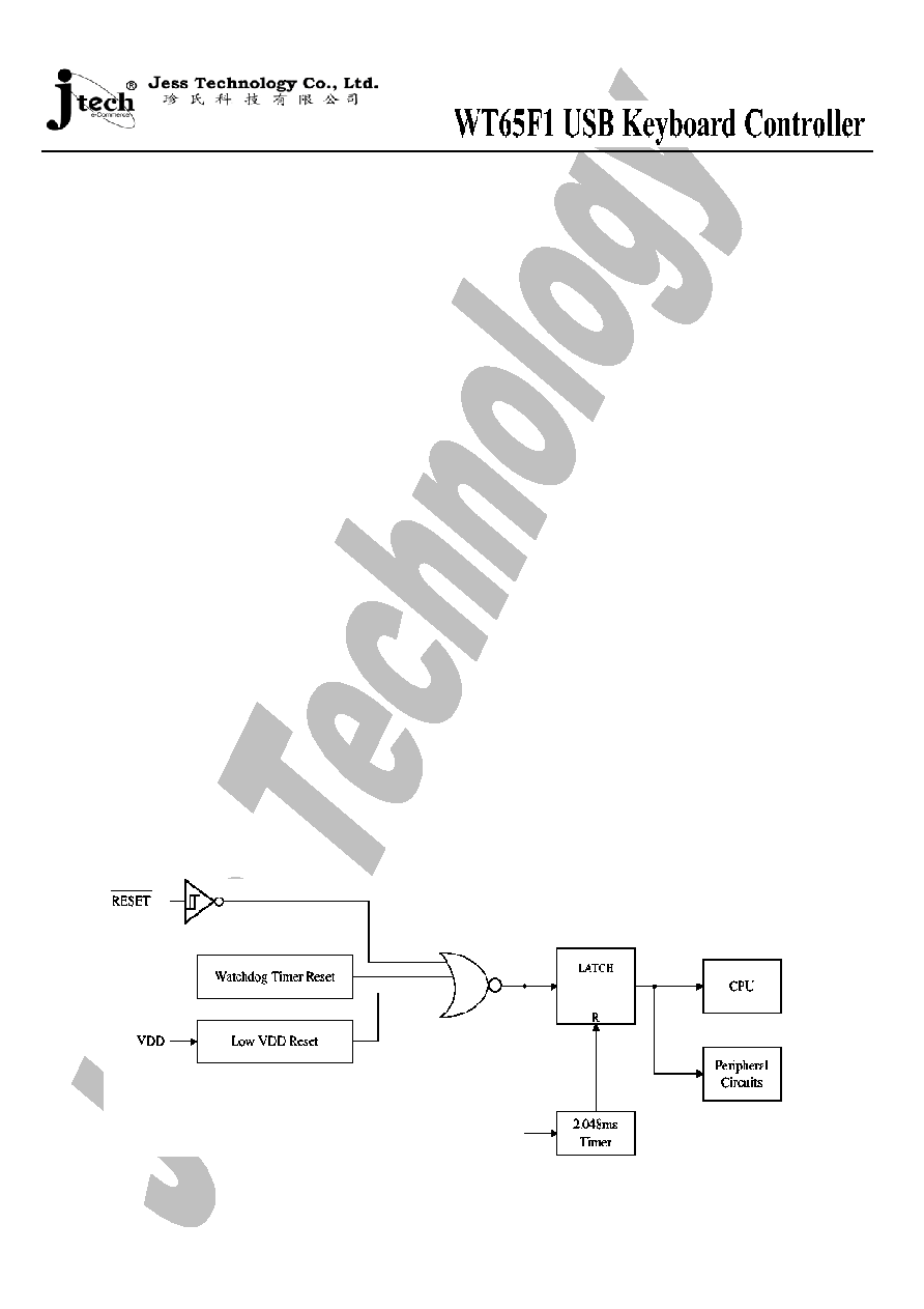
5
External Reset
A low level on the/RESET (NRST) pin will generate reset.
Low VDD Voltage Reset
When VDD is below 3.7V (typical), an internal reset signal is generated. The reset signal will last 2.048 ms after the voltage
is higher than 3.7V (typical)
Watchdog Timer Reset
If a time-out happens when watchdog timer is enabled, a reset pulse is generated. Please refer watchdog timer section for
more information.
General Purpose I/O Ports
Ports 0 to 2 provide 24 general purpose I/O pins that can be read or written. Each port (8 bits) can be configured as inputs
with internal pull-ups, or traditional CMOS outputs. Ports 0 to 2 are considered low current drive with typical current sink
capability of 10mA. The internal pull-up resistors are typically 25 Kohms.
Port 3 has eight general purpose I/O pins. Port 3 (8-bits) can be configured as inputs with internal pull-ups, or traditional
CMOS outputs. Port 3 offers high current drive with a typical current sink capability of 20 mA. The internal pull-up resistors
are typically 25 Kohms. After reset, all of the GPIO pins are set to input with the internal pull-up enabled.
Every GPIO port can be programmed as inputs with internal pull-ups, and traditional CMOS outputs. In addition, an input pin
causes an interrupt (if it is interrupt enabled) with negative polarity (a falling edge).
** P00, P01 might initialize as input without pull-u resistor. Only when the P0_CTRL = 0 and P0_DATA = 1, these pin (s)
might set as input and with internal pull-up resistor.
P0_CTRL: Port0 Direction Register
Name
Addr
R/W
Initial
Bit7
Bit6
Bit5
Bit4
Bit3
Bit2
Bit1
Bit0
P0_CTRL
00H
W
00H
P07OE
P06OE
P05OE
P04OE
P03OE
P02OE
P01OE
P00OE
P0_CTRL: Indicate Port0 direction.
P0nOE: =1: means output enable.
P0_DATA: Port0 Data Register
Name
Addr
R/W
Initial
Bit7
Bit6
Bit5
Bit4
Bit3
Bit2
Bit1
Bit0
R
P0_DATA
01H
W
00H
P07
P06
P05
P04
P03
P02
P01
P00
P0_DATA register shows the data read or write to Port0 [7:0]
P0n: =1: data read or write to Port0 [n] is 1