/home/web/doc/html/kec/190834
2005. 12. 15
1/7
SEMICONDUCTOR
TECHNICAL DATA
KHB5D0N50P/F
N CHANNEL MOS FIELD
EFFECT TRANSISTOR
Revision No : 2
General Description
This planar stripe MOSFET has better characteristics, such as fast
switching time, low on resistance, low gate charge and excellent
avalanche characteristics. It is mainly suitable for electronic ballast and
switching mode power supplies.
FEATURES
V
DSS
= 500V, I
D
= 5.0A
Drain-Source ON Resistance :
R
DS(ON)
=1.5
@V
GS
= 10V
Qg(typ.) = 28nC
MAXIMUM RATING (Tc=25 )
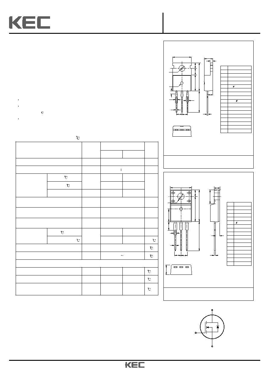
DIM
MILLIMETERS
TO-220AB
1.46
A
B
C
D
E
F
G
H
J
K
M
N
O
0.8 0.1
+
_
2.8 0.1
+
_
2.54 0.2
+
_
1.27 0.1
+
_
1.4 0.1
+
_
13.08 0.3
+
_
3.6 0.2
+
_
+
_
9.9 0.2
+
_
9.2 0.2
+
_
4.5 0.2
+
_
2.4 0.2
15.95 MAX
1.3+0.1/-0.05
0.5+0.1/-0.05
3.7
1.5
A
F
B
J
G
K
M
L
L
E
I
I
O
C
H
N
N
Q
D
Q
P
P
1. GATE
2. DRAIN
3. SOURCE
1
2
3
* : Drain current limited by maximum junction temperature.
G
D
S
DIM MILLIMETERS
TO-220IS
A
A
B
B
C
C
D
D
E
E
F
F
G
G
H
H
1.47 MAX
13.0 MAX
J
J
K
K
L
L
M
M
M
N
N
O
O
P
Q
Q
1
2
3
1. GATE
2. DRAIN
3. SOURCE
3.18 0.1
+
_
0.8 0.1
+
_
3.3 0.1
+
_
0.5 0.1
+
_
10.16 0.2
+
_
15.87 0.2
+
_
12.57 0.2
+
_
2.54 0.2
+
_
2.54 0.2
+
_
2.76 0.2
+
_
6.68 0.2
+
_
4.7 0.2
+
_
3.23 0.1
+
_
6.5
P
CHARACTERISTIC
SYMBOL
RATING
UNIT
KHB5D0N50P KHB5D0N50F
Drain-Source Voltage
V
DSS
500
V
Gate-Source Voltage
V
GSS
30
V
Drain Current
@T
C
=25
I
D
5.0
5.0*
A
@T
C
=100
2.9
2.9*
Pulsed (Note1)
I
DP
20
20*
Single Pulsed Avalanche Energy
(Note 2)
E
AS
390
mJ
Repetitive Avalanche Energy
(Note 1)
E
AR
9.2
mJ
Peak Diode Recovery dv/dt
(Note 3)
dv/dt
3.5
V/ns
Drain Power
Dissipation
Tc=25
P
D
73
38
W
Derate above 25
0.74
0.3
W/
Maximum Junction Temperature
T
j
150
Storage Temperature Range
T
stg
-55 150
Thermal Characteristics
Thermal Resistance, Junction-to-Case
R
thJC
1.71
3.31
/W
Thermal Resistance, Case-to-Sink
R
thCS
0.5
-
/W
Thermal Resistance, Junction-to-
Ambient
R
thJA
62.5
62.5
/W
2005. 12. 15
2/7
KHB5D0N50P/F
Revision No : 2
ELECTRICAL CHARACTERISTICS (Tc=25 )
CHARACTERISTIC
SYMBOL
TEST CONDITION
MIN.
TYP.
MAX.
UNIT
Static
Drain-Source Breakdown Voltage
BV
DSS
I
D
=250 A, V
GS
=0V
500
-
-
V
Breakdown Voltage Temperature Coefficient
BV
DSS
/ T
j
I
D
=250 A, Referenced to 25
-
0.6
-
V/
Drain Cut-off Current
I
DSS
V
DS
=500V, V
GS
=0V,
-
-
1
A
Gate Threshold Voltage
V
th
V
DS
=V
GS
, I
D
=250 A
2.0
-
4.0
V
Gate Leakage Current
I
GSS
V
GS
= 30V, V
DS
=0V
-
-
100
nA
Drain-Source ON Resistance
R
DS(ON)
V
GS
=10V, I
D
=2.5A
-
1.19
1.5
Dynamic
Total Gate Charge
Q
g
V
DS
=400V, I
D
=5A
V
GS
=10V (Note4,5)
-
28
37
nC
Gate-Source Charge
Q
gs
-
4
-
Gate-Drain Charge
Q
gd
-
12
-
Turn-on Delay time
t
d(on)
V
DD
=250V
R
L
=50
R
G
=25
(Note4,5)
-
-
40
ns
Turn-on Rise time
t
r
-
-
50
Turn-off Delay time
t
d(off)
-
-
200
Turn-off Fall time
t
f
-
-
50
Input Capacitance
C
iss
V
DS
=25V, V
GS
=0V, f=1.0MHz
-
-
1100
pF
Reverse Transfer Capacitance
C
rss
-
-
32
Output Capacitance
C
oss
-
-
115
Source-Drain Diode Ratings
Continuous Source Current
I
S
V
GS
<V
th
-
-
5
A
Pulsed Source Current
I
SP
-
-
20
Diode Forward Voltage
V
SD
I
S
=5A, V
GS
=0V
-
-
1.5
V
Reverse Recovery Time
t
rr
I
S
=5A, V
GS
=0V,
dIs/dt=100A/ s
-
330
-
ns
Reverse Recovery Charge
Q
rr
-
1.5
-
C
Note 1) Repetivity rating : Pulse width limited by junction temperature.
Note 2) L=21.5mH, I
S
=5A, V
DD
=50V, R
G
=25 , Starting T
j
=25 .
Note 3) I
S
5A, dI/dt 100A/ s, V
DD
BV
DSS
, Starting T
j
=25 .
Note 4) Pulse Test : Pulse width 300 s, Duty Cycle 2%.
Note 5) Essentially independent of operating temperature.
2005. 12. 15
3/7
KHB5D0N50P/F
Revision No : 2
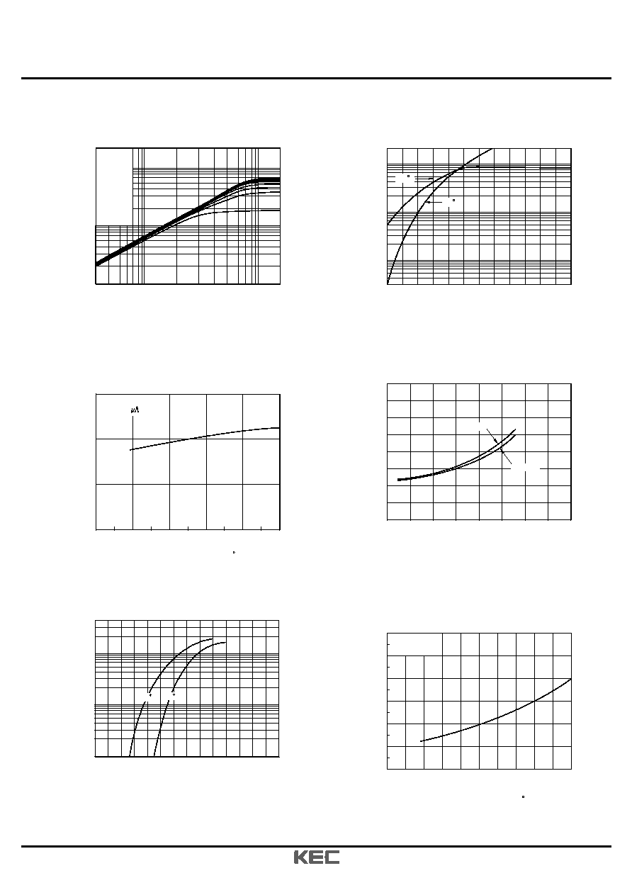
Gate - Source Voltage V
GS
(V)
I
D
- V
DS
Drain - Source Voltage V
DS
(V)
Drain Current I
D
(A)
10
0
10
1
10
-1
10
0
10
1
10
0
10
-1
10
1
6
8
4
10
5
7
9
I
D
- V
GS
R
DS(ON)
- I
D
Drain Current I
D
(A)
Drain Current I
D
(A)
On - Resistance R
DS(ON)
(
)
I
S
- V
SD
0.2
0.4
0.8
1.0
1.2
1.6
1.4
0.6
Reverse Drain Current I
S
(A)
0
1
3
2
4
0
10
4
16
12
6
2
14
8
Source - Drain Voltage V
SD
(V)
V
GS
= 20V
V
GS
= 10V
10
0
10
-1
10
1
V
GS
TOP : 15.0 V
10.0 V
9.0 V
8.0 V
7.0 V
6.0 V
5.5 V
5.0 V
Bottom: 4.5 V
Normalized Threshold Voltage V
th
V
th
- Tj
R
DS(ON)
- Tj
-100
-50
0.0
0.5
1.5
1.0
0
50
100
150
Junction Temperture Tj ( )
0
50
-100
-50
100
150
Normalized On Resistance
Junction Temperature Tj ( )
C
0.0
0.5
3.0
2.5
1.0
1.5
2.0
C
V
GS
= 10V
I
D
= 2.5A
V
GS
= 0V
I
DS
= 250
25
C
150
C
150 C
25 C
2005. 12. 15
4/7
KHB5D0N50P/F
Revision No : 2
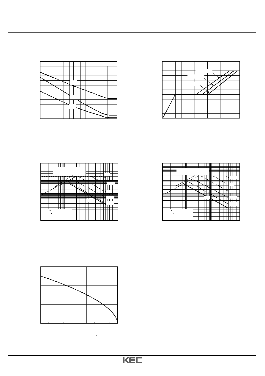
Gate - Charge Qg (nC)
C - V
DS
Drain - Source Voltage V
DS
(V)
0
12
10
6
2
4
8
10
5
30
25
20
15
0
Qg- V
GS
Capacitance (pF)
Gate - Source Voltage V
GS
(V)
0
500
1000
750
250
1250
1500
10
0
10
1
Frequency = 1MHz
I
D
= 5A
V
DS
= 250V
V
DS
= 400V
V
DS
= 100V
Coss
Ciss
Crss
Drain Current I
D
(A)
Drain - Source Voltage V
DS
(V)
Safe Operation Area
10
1
10
1
10
-1
10
-2
10
0
10
0
10
2
10
2
10
3
Drain Current I
D
(A)
Drain - Source Voltage V
DS
(V)
Safe Operation Area
10
1
10
1
10
-1
10
0
10
0
10
2
10
-2
10
2
DC
100 ms
10
�
s
10 ms
1
�
s
10
�
s
0
3
6
1
2
4
5
75
150
125
50
100
25
Drain Current I
D
(A)
(KHB5D0N50P)
(KHB5D0N50F)
C
Junction Temperature Tj ( )
I
D
- T
j
DC
10
�
s
1ms
100ms
10ms
100
�
s
Tc= 25
T
j
= 150
Single nonrepetitive pulse
C
C
Operation in this
area is limited by R
DS(ON)
Operation in this
area is limited by R
DS(ON)
Tc= 25
T
j
= 150
Single nonrepetitive pulse
C
C
2005. 12. 15
5/7
KHB5D0N50P/F
Revision No : 2
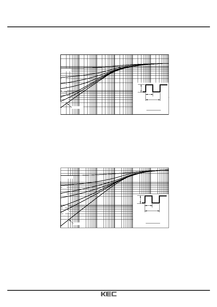
{KHB5D0N50P}
{KHB5D0N50F}
Square Wave Pulse Duration (sec)
Square Wave Pulse Duration (sec)
R
th
Normalized Transient Thermal Resistance
Normalized Transient Thermal Resistance
R
th
10
-5
10
-3
10
-2
10
-1
10
0
10
1
10
-4
10
-2
10
-1
10
0
- Duty Factor, D= t
1
/t
2
T
j(max)
- T
c
- R
thJC
=
P
D
t
1
t
2
P
DM
10
-5
10
-3
10
-2
10
-1
10
0
10
1
10
-4
10
-2
10
-1
10
0
- Duty Factor, D= t
1
/t
2
T
j(max)
- T
c
- R
thJC
=
P
D
t
1
t
2
P
DM
Duty=0.5
Single Pulse
0.05
0.02
0.01
0.2
0.1
Duty=0.5
Single Pulse
0.05
0.02
0.01
0.2
0.1