Kentron Technologies, Inc.
155 West Street
Wilmington, MA 01887
Phone: (978) 988-9100
Fax (978) 988-5550
www.kentrontech.com
32MX 72 UNBUFFERED FEMMA SDRAM SODIMM
SDRAM FEMMA SODIMM MODULE
256 MByte (32M x 72) SDRAM
Unbuffered ECC 144 Pin SODIMM
General Description:
This memory module is a high density 256 Megabyte Unbuffered synchronous dynamic RAM
module organized as 32M x 72 in a 144-pin ECC Small Outline Dual In-Line Memory Module
(SODIMM) package. The module utilizes eighteen (18) 4Mx4X8 128Mbit SDRAM devices in a
TSOP II 400 mil package. A zero delay buffer drives the input clock to all SDRAM devices.
A 256 Byte Serial EEPROM contains the module configuration information. The EEPROM can
be configured to a customer's specifications.
These modules offer substantial advances in SDRAM operating performance, including the
ability to synchronously burst data at a high rate with automatic column-address generation,
interleave between internal banks in order to hide precharge time, and the capability to
randomly change column address on each clock cycle during burst.
Features:
High density: 256 MB (32M x 72)
Cycle time: 10 ns (100 MHz)
7.5 ns (133 MHz)
JEDEC Standard 144 Pin Unbuffered SDRAM SODIMM Pinout
PC133 and PC100 Compliant
Single power supply of 3.3V � 10%
Serial Presence Detect
LVTTL Compatible I/O and Clock
Unbuffered Control and Address Lines
ECC operation
On-board PLL Clock Driver (2 msec settling time)
4K Refresh in 64ms (15.6 usec per row)
Auto Precharge and Auto Refresh Modes handled by SDRAM Devices
Programmable Burst Type, Burst Length and CAS Latency of SDRAM Devices
Internal Pipeline Operation
Fully Synchronous � all signals registered on positive edge of system clock
Package Height: 1.25 inches (+/- 10mils)
Patented
Kentron Technologies, Inc. (978) 988-9100 Page 2
Rev. 12/01
32M X 72 UNBUFFERED FEMMA SDRAM SODIMM
Operating Features:
The FEMMA SDRAM SODIMM utilizes a clock input for the synchronization. Each operation of
the SDRAM is determined by commands and all operations are referenced to a positive clock
edge. CAS Latency defines the delay from when a Read Command is registered on a rising
clock edge to when the data from the Read Command becomes available at the outputs. The
CAS latency is expressed in terms of clock cycles. This specific DIMM supports 3 and 2 clock
cycles.
The burst mode is a very high-speed access mode utilizing an internal column address
generator. Once a column address for the first access is set, following addresses are
automatically generated by the internal column address counter.
All control and address signals are supplied from the chipset through an unbuffered path to the
SDRAMs. CK0 supplied by the motherboard feeds into a Phase Lock Loop (PLL) on the module
to drive all sixteen SDRAMs.

Kentron Technologies, Inc. (978) 988-9100 Page 3
Rev. 12/01
32M X 72 UNBUFFERED FEMMA SDRAM SODIMM
Absolute Maximum Ratings*:
Item
Symbol
Rating
Unit
Supply voltage (V
CC
Relative to V
SS
)
V
CC
-1.0 to +4.6
V
Input/Output Voltage
V
I/O
-1.0 to +4.6
V
Operating temperature
T
opr
0 to +70
�C
Storage temperature
T
stg
-55 to +125
�C
Short circuit output current
I
out
�50
mA
* Permanent device damage may occur if absolute maximum ratings are exceeded. Functional operation
should be restricted to the conditions as detailed in the sections of this data sheet. Exposure to absolute
maximum rating conditions for extended periods may affect device reliability.
Recommended Operating Conditions:
(Voltage referenced to V
CC
. T
A
= 0 to 70 �C)
Item
Symbol
Min.
Typ.
Max.
Unit
Supply voltage
V
DD
3.1
3.3
3.5
V
Input high voltage
V
IH
2.0
-
V
DD
+0.3
V
Input low voltage
V
IL
-0.3
-
0.8
V
Operating Temperature
T
A
0
+25
+70
�C
Capacitance:
(TA=25�C, Vcc=3.3V�0.3V)
Parameter
Symbol
Max.
Unit
Input capacitance (Address, /WE, CKE0,1 , /CAS)
Input capacitance ( /CS0~/CS1)
C
IN
C
IN
88
29
pF
pF
Input capacitance (/DQMBs)
C
IN
15
pF
Input capacitance (CK0)
C
IN
5
pF
Input capacitance (/RAS)
C
IN
88
pF
Input/Output capacitance (DQ0~DQ63, CB0~CB7)
C
I/O
18
pF
Kentron Technologies, Inc. (978) 988-9100 Page 4
Rev. 12/01
32M X 72 UNBUFFERED FEMMA SDRAM SODIMM
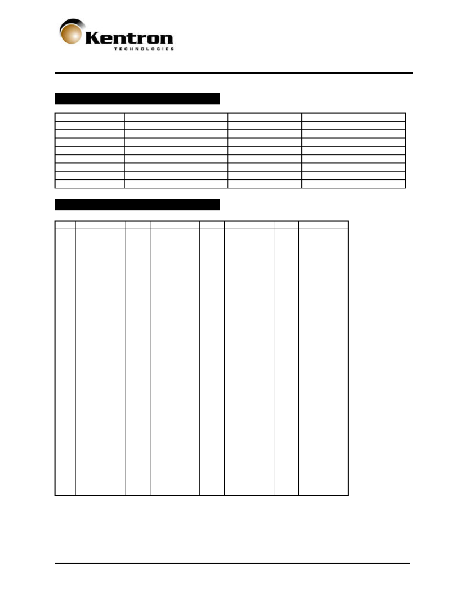
Pin Names:
CK0-CK2
Clock Inputs
DQ0-DQ63
Data Inputs/Outputs
CKE0-CKE1
Clock Enables
CB0-CB7
ECC Data Input/Output
/RAS
Row Address Strobe
/DQMB0-/DQMB7
Data Mask Enables
/CAS
Column Address Strobe
V
DD
Power supply
/WE
Write Enable
V
SS
Ground
/S0-/S1
Chip Select
SCL
Serial Clock
A0-A11
Address Inputs
SDA
Serial Data Input/Output
BA0, BA1
SDRAM Bank Select
SA0-SA2
Decode Input
NC or DU
No Connect
WP
Write Protect for SPD
SDRAM Pinout:
No.
Designation
No.
Designation
No.
Designation
No.
Designation
1
Vss
37
DQ8
73
NU
109
A9
2
Vss
38
DQ40
74
CK1
110
BA1
3
DQ0
39
DQ9
75
Vss
111
A10/AP
4
DQ32
40
DQ41
76
Vss
112
A11
5
DQ1
41
DQ10
77
CB2
113
V
DD
6
DQ33
42
DQ42
78
CB6
114
V
DD
7
DQ2
43
DQ11
79
CB3
115
DQMB2
8
DQ34
44
DQ43
80
CB7
116
DQMB6
9
DQ3
45
V
DD
81
V
DD
117
DQMB3
10
DQ35
46
V
DD
82
V
DD
118
DQMB7
11
V
DD
47
DQ12
83
DQ16
119
Vss
12
V
DD
48
DQ44
84
DQ48
120
Vss
13
DQ4
49
DQ13
85
DQ17
121
DQ24
14
DQ36
50
DQ45
86
DQ49
122
DQ56
15
DQ5
51
DQ14
87
DQ18
123
DQ25
16
DQ37
52
DQ46
88
DQ50
124
DQ57
17
DQ6
53
DQ15
89
DQ19
125
DQ26
18
DQ38
54
DQ47
90
DQ51
126
DQ58
19
DQ7
55
Vss
91
Vss
127
DQ27
20
DQ39
56
Vss
92
Vss
128
DQ59
21
Vss
57
CB0
93
DQ20
129
V
DD
22
Vss
58
CB4
94
DQ52
130
V
DD
23
DQMB0
59
CB1
95
DQ21
131
DQ28
24
DQMB4
60
CB5
96
DQ53
132
DQ60
25
DQMB1
61
CK0
97
DQ22
133
DQ29
26
DQMB5
62
CKE0
98
DQ54
134
DQ61
27
V
DD
63
V
DD
99
DQ23
135
DQ30
28
V
DD
64
V
DD
100
DQ55
136
DQ62
29
A0
65
RAS
101
V
DD
137
DQ31
30
A3
66
CAS
102
V
DD
138
DQ63
31
A1
67
WE
103
A6
139
Vss
32
A4
68
CKE1
104
A7
140
Vss
33
A2
69
S0
105
A8
141
SDA
34
A5
70
NC (A12)
106
BA0
142
SCL
35
Vss
71
S1
107
Vss
143
V
DD
36
Vss
72
NC (A13)
108
Vss
144
V
DD

Kentron Technologies, Inc. (978) 988-9100 Page 5
Rev. 12/01
32M X 72 UNBUFFERED FEMMA SDRAM SODIMM
DC Characteristics:
(
V
DD
= 3.3V�.3V, V
SS
=0V, T
A
=0 to + 70�C)
Parameter
1
Symbol
133MHz
Max.
100MHz
Max.
Unit
Operating current
(No Burst, T
CK
=min. T
RC
=min. Single Bank)
I
CC1
1480
1200
mA
Precharge Standby Current
(CKE=V
IL
, T
CK
= min. All banks idle)
(CKE=V
IH
, T
CK
= min. All banks idle)
I
CC2
16
256
16
256
mA
Active Standby Current
(CKE=V
IL
, T
CK
= min. One bank active)
(CKE=V
IH
, T
CK
= min. One bank active)
I
CC3
90
560
90
560
mA
Burst Mode Current (t
CK
=min.)
I
CC4
1700
1400
mA
Refresh Current (per DIMM bank)
(t
CK
=min., t
RC
=min., t
RRD
=min., Auto Refresh)
I
CC5
2000
2000
mA
Self Refresh Current (all DIMM banks, CKE=V
IL
)
Low Power
2
I
CC6
56
30
56
30
mA
1
Typical Actual values run lower that Max Spec'Ed Values.
2
Based on Low Power SDRAM