
KING BILLION ELECTRONICS CO., LTD
HE83139
HE80000 SERIES
1
V1.0
A. HE83139 Introduction
HE83139 is a member of 8-bit Micro-controller series developed by King Billion Electronics Ltd. This
IC provides 512 pixels LCD display and built-in OP comparator can be used with light, voice,
temperature and humility sensor or used to detect the battery low. The 7-bit current-type D/A converter
and PWM drive output provide the complete speech output mechanism.
The 64K bytes ROM size can be used to store 15 seconds speech data. It can be applicable to the LCD
game, medium level educational toy, lower second voice recording system or used with external
command mode SRAM or Flash RAM for higher second voice recording etc.
The instruction sets of HE80000 series are quite easy to learn and simple to use. Only about thirty
instructions with four-type addressing mode are provided. Most of instructions take only 3 oscillator
clocks (machine cycles). The performance of HE83750S is enough for most of battery operation
system.
B. HE83139 Features
Operation Voltage:
2.4V ~ 5.5V
System Clock
4MHz ~ 8MHz
Clock Source:
Internal/External Fast clock, Internal/External slow clock
Dual Clock System
Normal (Fast) clock
32.768KHz ~ 8MHz
Slow
clock
32.768
KHz
Operation Mode DUALFASTSLOWIDLESLEEP Mode.
Internal
ROM: 64K
Bytes.
Internal
RAM: 2K
Bytes.
Watch dog timer.
16 Bi-directional I/O ports.
512 pixels LCD driver with A, B type choice
LCD Bias : 1/5
LCD Charge Pump: 1 or 1.5 times of VDD
One 7-bits current-type DAC output.
One built-in OP comparator.
PWM device.
Built-in DTMF Generator.
Speech recognition function
Two external interrupts and three internal timer interrupts.
Two 16-bit timers.
Instruction set 32 instructions, 4 addressing mode.
10-bit DATA POINTER for RAM and 16-bit
TABLE POINTER for ROM.
KING BILLION ELECTRONICS CO., LTD
HE83139
HE80000 SERIES
2
V1.0
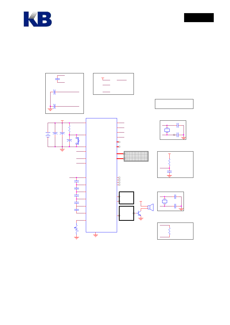
C. Application Circuit
VDD
VDD
VDD
VDD
SXO
LC2
LC1
LV1
LC2
FXI
SXI
LV3
LV3
LV3
SXI
FXO
FXI
SXO
LC1
LC2
SXO
SXO
LC1
FXI
LV1
LV1
FXO
SXI
C5
0.1uF
VDD
FXO
FXI
SXI
SXO
LC1
LC2
LV1
LV3 < 9 Volt
LVG
TS
TP
_
P
VO
PWMP
PWMN
COM[15:0]
SEG[31:0]
PRTD[7:0]
PRT17[7:0]
RSTP_N
GND
OPIN
OPIP
OPO
LR4
LR3
LR2
LR1
LR0
DAO
SW1
RESET
BATTERY1
3V
C1
0.1uF
C6
0.1uF
C2
0.1uF
2MHZ
C3
0.1uF
C4
0.1uF
32.768K
C3
0.1uF
20P
R1
50K
20P
C2
100uF
C7 0.1uF
Q1
NPN
20P
C1
0.1uF
R > 8.2 KOhm
20P
SP1
SPEAKER
VR1
?K Ohm
C9 0.1uF
C: Please Ref. AN016
R: Please ref. AN016
Twice Charge Pump is selected
LCD Max. Voltage=LV3=3/2*VDD
No Capacitor
1/5 BAIS
CONFIGURATION
Buzzer
or
Speaker
Circuit
External Slow Clock:
RC osc.
External Fast Clock:
Crystal osc.
Passive
Bias &
Filter
Circuit
External Slow Clock:
Crystal osc.
External Fast Clock:
RC osc.
Floating
Please Refer
AN022 for Speech
Output Circuit
No External Parts is
necessary if user adopt
Internal Fast RC Clock
LCD PANEL
Twice Charge Pump is selected
LCD Max. Voltage=LV3=VDD