 | –≠–ª–µ–∫—Ç—Ä–æ–Ω–Ω—ã–π –∫–æ–º–ø–æ–Ω–µ–Ω—Ç: HF88M32 | –°–∫–∞—á–∞—Ç—å:  PDF PDF  ZIP ZIP |

King Billion Electronics Co., Ltd
HF88M32
April 28, 2003
1
V1.0
This specification is subject to change without notice. Please contact sales person for the latest
version before use.
Preliminary Product Specification
Product Name
Command Interface 8M-Bit Mask ROM with Expansion I/O
KB Doc. No.
HF88M32
KB Product. No.
HF88M32
- Table of Contents ≠
1. General Description _____________________________________________________2
2. Features ______________________________________________________________2
3. Functional block diagram ________________________________________________3
4. Pin Description_________________________________________________________3
5. Device Operation _______________________________________________________4
5.1.
Retrieve data in Data File _________________________________________________ 6
5.2.
Loading the Address Counter______________________________________________ 6
5.3.
Sequential Read Mode and Auto Increment of Address Counter _________________ 7
5.4.
Output data to External I/O _______________________________________________ 7
5.5.
Reading Input pin status__________________________________________________ 7
5.6.
Retrieving the Contents of Expansion I/O registers ____________________________ 8
6. Timing Diagrams _______________________________________________________8
6.1.
Data File Read Cycle _____________________________________________________ 8
6.2.
Interrupted by I/O when Loading Address Counter ___________________________ 9
6.3.
Setting and Reading the I/O Mode for P0 and P1 _____________________________ 9
6.4.
Reading P0 and P1 in Mixed-I/O Mode______________________________________ 9
6.5.
Reading the input pins __________________________________________________ 10
6.6.
Output to P0 and P1 ____________________________________________________ 10
7. Absolute Maximum Rating ______________________________________________ 11
8. AC Electrical Characteristics ____________________________________________ 11
9. DC Electrical Characteristics ____________________________________________12
10.
Application Circuit Diagram ___________________________________________12

King Billion Electronics Co., Ltd
HF88M32
April 28, 2003
2
V1.0
This specification is subject to change without notice. Please contact sales person for the latest
version before use.
1. General Description
The HF88M32 is a command interfaced 4M x 8 bit Mask ROM. It features command mode
interface with external CPU or MCU. In other words, it uses only 8-bit data bus and a few
additional control pins to load addresses and provide the ROM access as well as expansion
I/O ports capability. This design not only reduces pin count required to access data in ROM
dramatically but also allows for systems expansion to higher capacity memories while using
the existing board design. The application areas include voice, graphic, data storage in
consumer product.
2. Features
Data File Mode with only 11 pin interface
Sixteen-bit Expansion I/O pins with three-state mode
Voltage range: 2.4 ~ 3.6V
Organization
- Memory Cell Array: 4M x 8
Sequential Read Operation in Data File Operation Mode
- Sequential Access : 100 ns (min.) at V
DD
= 3.3V
Command/Address/Data Multiplexed I/O port
Low Operation Current (Typical)
- 10
µA standby mode current.
- 30 mA active read current at 100 ns cycle time.
Package: bare chip
King Billion Electronics Co., Ltd
HF88M32
April 28, 2003
3
V1.0
This specification is subject to change without notice. Please contact sales person for the latest
version before use.
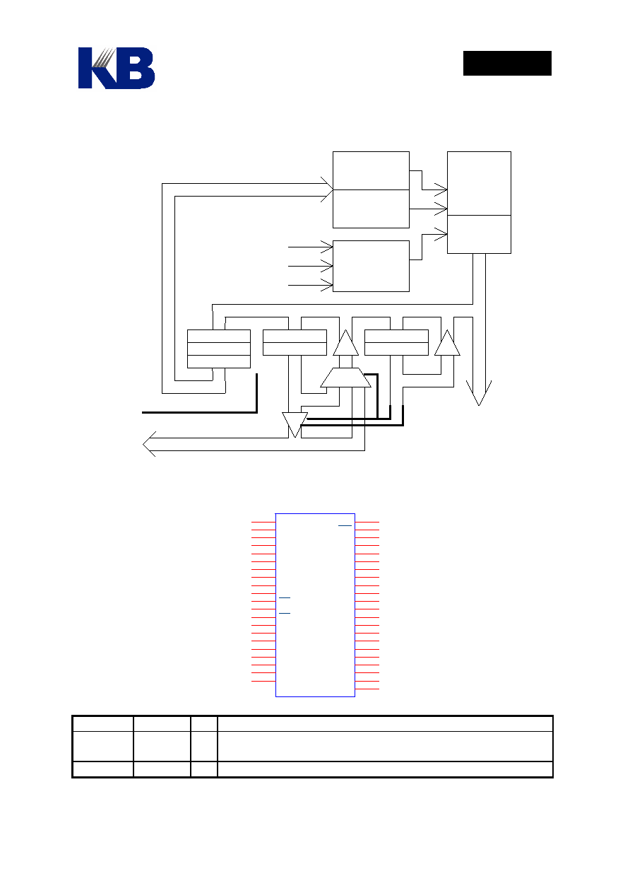
3. Functional block diagram
MEMORY
CELL
ARRAY
SENSE
AMP.
OEn
X BUFFER &
DECODER
[D7.. D0]
CONTROL
LOGIC
Y BUFFER &
DECODER
CEn
[P00..P07]
[P10..P17]
[A21..A0]
AC0
AC1
AC2
P0
DIR0
P1
DIR1
WEn
RS2..RS0
4. Pin Description
HF88M32
10
9
8
7
6
5
4
3
41
40
39
38
37
36
35
34
33
11
13
32
14
16
18
20
23
25
27
29
22
12
2
1
42
15
17
19
21
24
26
28
30
31
43
P00
P01
P02
P03
P04
P05
P06
P07
P10
P11
P12
P13
P14
P15
P16
P17
RS0
CE
OE
NC
D0
D1
D2
D3
D4
D5
D6
D7
VCC
GND
RS1
RS2
WE
NC
NC
NC
NC
NC
NC
NC
NC
GND
NC
Symbol Pin
No. I/O
Description
RS0~RS2 33, 2, 1
I Register Select pins RS2 ~ RS0 for accessing ROM data,
Address Counter, as well as expansion I/O ports.
P07 ~ P00 3 ~ 10
I/O Bi-directional I/O port P0.

King Billion Electronics Co., Ltd
HF88M32
April 28, 2003
4
V1.0
This specification is subject to change without notice. Please contact sales person for the latest
version before use.
Symbol Pin
No. I/O
Description
CEn
11
I The CEn (Chip Enable) input is the device selection and power
control for internal Mask ROM array. Whenever CEn goes high,
the internal Mask ROM will enter standby (power saving) mode
and accesses to internal registers are inhibited. Otherwise, it is
in active mode and the contents of the ROM and registers can
be accessed. Please note that only accesses to the internal
registers are inhibited, but the status of I/O registers are not
affected by the CEn pin and will remain unchanged. CEn is also
useful to uniquely select a certain device for applications where
multiple-chip array is required.
GND
12, 31
P Negative power supply input pin.
OEn
13
I OEn (Output Enable) is the output control which gates ROM
array data, expansion I/O ports, Direction Registers to the data
I/O pins D7 ~ D0. The internal Address Counter will
automatically increment by one with each rising edge of OEn
pin in Sequentially Read mode.
VCC
22
P Postive power supply input pin.
D7 ~ D0
14, 16,
18, 20,
23, 25,
27, 29
I/O The Bi-directional Data I/O pins are used to set starting
addresses, set the Extension I/O Direction and Output Registers,
and to output ROM array data during read operations, contents
of I/O Registers and status of input pins. The D7 ~ D7 float to
high-impedance when the chip is deselected (CEn high) or
when the outputs are disabled.
P17 ~ P10 34 ~ 41 I/O Bi-directional I/O port P1.
WEn
42
I WEn controls writing to internal registers such as the Output
Port Registers, Direction Registers, Address Counter and Data
on D7 ~ D0 are latched on the rising edge of the WE pulse.
5. Device Operation
The device provides the capability of accessing the contents of ROM array by external MCU
not through standard address and data bus configuration but through minimal number of 8-bit
data bus and control pins. Only 11 pins D7 ~ D0, CEn, OEn, WEn are required to use the
device as a Data File device. By fixing the RS2 to `0', only CEn, WEn, OEn and D0 ~ D7 are
required to access the ROM array data.
The CEn pin is device selection pin to uniquely select one device when more than one device
are used in parallel and control the access to Mask ROM contents and internal registers.
Whenever CEn goes high, the internal Mask ROM will enter standby (power saving) mode
and accesses to internal registers are inhibited. Otherwise, it is in active mode. Therefore,
when accessing contents of ROM is not intended, CEn should stay at `1' to conserve the
power.

King Billion Electronics Co., Ltd
HF88M32
April 28, 2003
5
V1.0
This specification is subject to change without notice. Please contact sales person for the latest
version before use.
In addition to Data File mode, the device also provides the expansion I/O capability. Two
ports of I/O pins (8 bit each) are provided. The I/O ports can be configured to function as
output pin or high-impedance input pins. Only 14 pins, CEn, WEn, OEn, RS2, RS1 and D0 ~
D7 are required to provide the Data File function and full access to two I/O ports.
There are seven internal registers used to provide the functionality of Data file as well as
Expansion I/O capability. These registers are selected by RS2 ~ RS0. All registers are 8-bit
wide except AC2. AC2 ~ AC0 are write-only and constitute the complete 22-bit Address
Counter used as pointer to the data. While the P0, P1, DIR0 and DIR1 can be read as well as
written. Their initial values are as indicated in the following table. When RS2 = `0', the RS1
~ RS0 are ignored, the Address Counter can be loaded or contents of Data File can be read.
This is to reduce the required pin needed for external MCU to interface with the Device and
also simplify the procedure for loading the address counter.
The P0, P1, DIR0, and DIR1 are used for expansion I/O registers. The P0 and P1 are output
registers of Expansion I/O and DIR0 and DIR1 are the Direction Registers that determine the
I/O mode of P0 and P1. Each pin can be configured as output or input mode individually by
setting or resetting the corresponding pin of the DIR registers. Initially, both P0 and P1 are
default to input mode at `Hi' state.
DIR00
RS = 100 & OEn = '0'
RS = 101 & OEn = '0'
RS = 111 & OEn = '0'
RS = 110 & OEn = '0'
P00
D0
P10
1
0
Q
D
Q
D
P00
DIR00
1
0
Q
D
DIR10
Q
P10
D