
King Billion Electronics Co., Ltd
SF23C3200
April 28, 2003
1
V1.0
This specification is subject to change without notice. Please contact sales person for the latest
version before use.
Preliminary Product Specification
Product Name
32 Mb Mask Programmable ROM
KB Doc. No.
SF23C3200
KB Product. No.
SF23C3200
- Table of Contents -
1. General Description _____________________________________________________1
2. Features ______________________________________________________________1
3. Functional block diagram ________________________________________________2
4. Pin Description_________________________________________________________2
5. Absolute Maximum Rating _______________________________________________3
6. AC Electrical Characteristics _____________________________________________3
7. DC Electrical Characteristics _____________________________________________4
1. General Description
The SF23C3200 is a fully static, 32 Mbit CMOS Mask Programmable ROM. This device
operates in wide operating range. It requires no external clock for its operation and suitable
for use with microprocessor program memory, and data memory (speech, graphic, etc).
2. Features
Operating range: 2.4V ~ 3.6V
Organization
- Memory Cell Array: 4M x 8 or 2M x 16 selectable by BYTEB pin
Low Operation Current (Typical)
- 10
µA standby mode current.
- 30 mA active read current at 100 ns cycle time.
Fully static operation
Tri-state outputs
Package: bare chip

King Billion Electronics Co., Ltd
SF23C3200
April 28, 2003
2
V1.0
This specification is subject to change without notice. Please contact sales person for the latest
version before use.
3. Functional block diagram
MEMORY
CELL
ARRAY
SENSE AMP.
OEn
X BUFFER &
DECODER
CONTROL
LOGIC
Y BUFFER &
DECODER
CEn
[A20..A-1]
[Q15..Q0]
BYTEB
4. Pin Description
SF23C3200
10
9
8
7
6
5
4
3
41
40
39
38
37
36
35
34
33
11
13
32
14
16
18
20
23
25
27
29
22
12
2
1
42
15
17
19
21
24
26
28
30
31
43
A0
A1
A2
A3
A4
A5
A6
A7
A8
A9
A10
A11
A12
A13
A14
A15
A16
CE
OE
BYTE
Q0
Q1
Q2
Q3
Q4
Q5
Q6
Q7
VCC
GND
A17
A18
A19
Q8
Q9
Q10
Q11
Q12
Q13
Q14
Q15/A-1
GND
A20
Symbol Pin
No. I/O
Description
A18, A17
1, 2
I Mask ROM Address input pins.
A7 ~ A0
3 ~ 10
I Mask ROM Address input pins.
CEn
11
I The CEn (Chip Enable) input is the device selection and power
control for internal Mask ROM array. Whenever CEn goes
high, the internal Mask ROM will enter standby (power saving)
mode. Otherwise, it is in active mode and the contents of the
ROM can be accessed.
GND
12
P Negative power supply input pin.

King Billion Electronics Co., Ltd
SF23C3200
April 28, 2003
3
V1.0
This specification is subject to change without notice. Please contact sales person for the latest
version before use.
OEn
13
I OEn (Output Enable) is the output control which gates ROM
array data onto the data output pins Q7 ~ Q0 in Byte mode
(BYTEB pin is at "low" state) or Q15A-1, Q14 ~ Q0 in Word
mode (BYTEB pin is at "high" state).
Q0,
Q1,
Q2,
Q3,
Q4,
Q5,
Q6,
Q7,
14,
16,
18,
20,
23,
25,
27,
29
O,
O,
O,
O,
O,
O,
O,
O,
Mask ROM array Data lower byte outputs drive Q7 ~ Q0 pins
during read operations (CEn and OEn are "low"). The Q7 ~ Q0
pins stay in high-Z when the chip is deselected (CEn high) or
when the outputs are disabled (OEn high).
Q8,
Q9,
Q10,
Q11,
Q12,
Q13,
Q14,
Q15A-1,
15,
17,
19,
21,
24,
26,
28,
30
O,
O,
O,
O,
O,
O,
O,
O/I,
Mask ROM data higher byte output pins when Word mode is
selected (BYTEB is at "high" level) during read operations
(CEn and OEn are "low"). They will be tri-stated when Byte
mode is selected (BYTEB at "low" level), the chip is deselected
(CEn high), the outputs are disabled (OEn high).
Q15A-1 is Mask ROM MSB Data output pin in Word mode
and LSB address pin in Byte mode.
VCC
22
P Positive power supply input pin.
GND
31
P Negative power supply input pin.
BYTEB 32 I
Byte/Word
mode
selection
input pin. Byte mode is selected
when it is at "low" state, otherwise Word mode is selected.
A16 ~ A8 33 ~ 41
I Mask ROM Address input pins.
A19, A20
42, 43
I Mask ROM Address input pins.
5. Absolute Maximum Rating
Items Symbol
Rating
Supply Voltage
V
CC
2.4 to 3.6 V
Input Voltage
V
IN
-0.3 to Vdd+0.3 V
Operating Temperature
T
OPR
-0 to 70
∞C
Storage Temperature
T
STR
-55 to 125
∞C
6. AC Electrical Characteristics
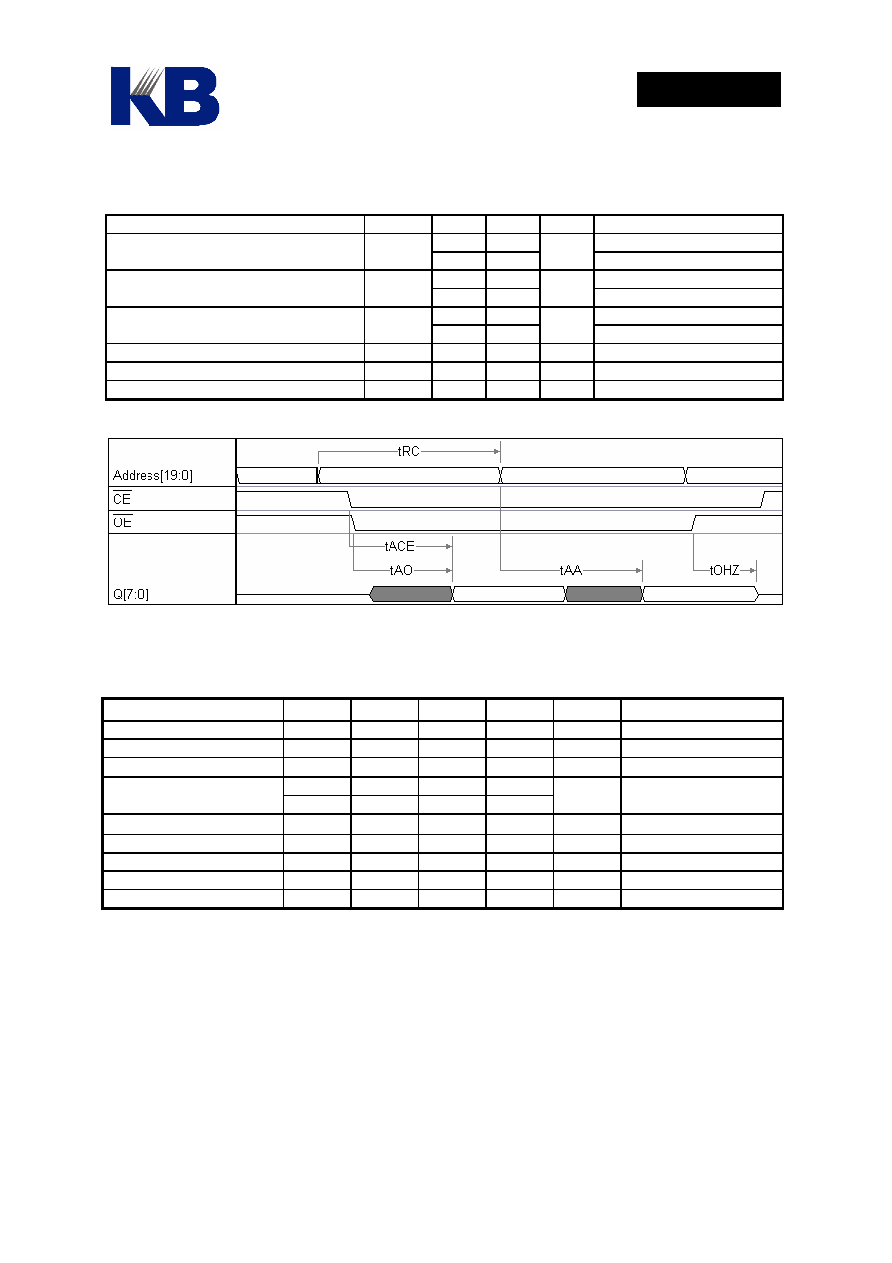
READ CYCLE:
There are two ways of accessing the ROM data. The first one is to assert the valid address on
the Address Bus, then assert CEn "low" to enable the ROM array. The access time in this
mode is specified as t
ACE
. The advantage of this access mode is that power consumption can
King Billion Electronics Co., Ltd
SF23C3200
April 28, 2003
4
V1.0
This specification is subject to change without notice. Please contact sales person for the latest
version before use.
be lowered. The second access mode keeps the CEn "low" while changes the addresses to
access the contents of ROM data. The access time in this way is specified as t
AA
.
Item Symbol
Min
Max
Unit
Condition
100
V
DD
= 3.0 V, no load
Read Cycle Time
t
RC
120
ns
V
DD
= 2.4V, no load
100
V
DD
= 3.0 V, no load
Chip Enable Access Time
t
ACE
120
ns
V
DD
= 2.4V, no load
100
V
DD
= 3.0 V, no load
Address Access Time
t
AA
120
ns
V
DD
= 2.4V, no load
Output Enable Time
t
OE
50
ns
Output or Chip Disable to Output High-Z
t
DF
20
ns
Output Hold from Address Change
t
OH
0 ns
7. DC Electrical Characteristics
(GND = 0V, V
CC
= 3.0 V, T
OPR
= 25
∞C unless otherwise noted)
Parameter Symbol
Min.
Typical
Max.
Unit Condition
Supply Voltage
V
CC
2.4 - 3.6 V
Operating Current
I
CC
- 30 - mA
No
load,
t
RC
@ 100 ns
Standby Current
I
STBY
- 10 -
µA
No load
V
IH
2/3 - 1
Input voltage
V
IL
0 - 1/3
V
DD
V
DD
= 2.4V ~ 3.6V
Input current leakage
I
IL
- - ± 10
µA
P0, P1 Output High Voltage
V
OH
2.4 -
- V
I
OH
= 0.4 mA
P0, P1 Output Low Voltage
V
OL
- - 0.4 V
I
OL
= 2.1 mA
D Output High Voltage
V
OH
2.4 -
- V
I
OH
= 1.4 mA
D Output Low Voltage
V
OL
- - 0.4 V
I
OL
= 3 mA