SPEC NO: DSAD1222
REV NO: V.1
DATE: MAR/24/2003
PAGE: 1 OF 4
APPROVED: J. Lu
CHECKED: Allen Liu
DRAWN: Z.Y.YANG
Package Dimensions
Features
l
3.0mm X 2.0mm, 1.4mm HIGH, ONLY MINIMUM
SPACE REQUIRED.
l
SUITABLE FOR COMPACT OPTOELECTRONIC
APPLICATIONS.
l
LOW POWER CONSUMPTION.
l
PACKAGE : 2000PCS / REEL.
Notes:
1. All dimensions are in millimeters (inches),
2. Tolerance is
±
0.25(0.01") unless otherwise noted.
3. Specifications are subject to change without notice.
3.0x2.0mm SURFACE MOUNT LED LAMP
AA3020MBCK BLUE
Description
The Blue source color devices are made with GaN
on SiC Light Emitting Diode.
Static electricity and surge damage the LEDS. It is
recommended to use a wrist band or anti-
electrostatic glove when handling the LEDs.
All devices, equipment and machinery must be
electrically grounded.

SPEC NO: DSAD1222
REV NO: V.1
DATE: MAR/24/2003
PAGE: 2 OF 4
APPROVED: J. Lu
CHECKED: Allen Liu
DRAWN: Z.Y.YANG
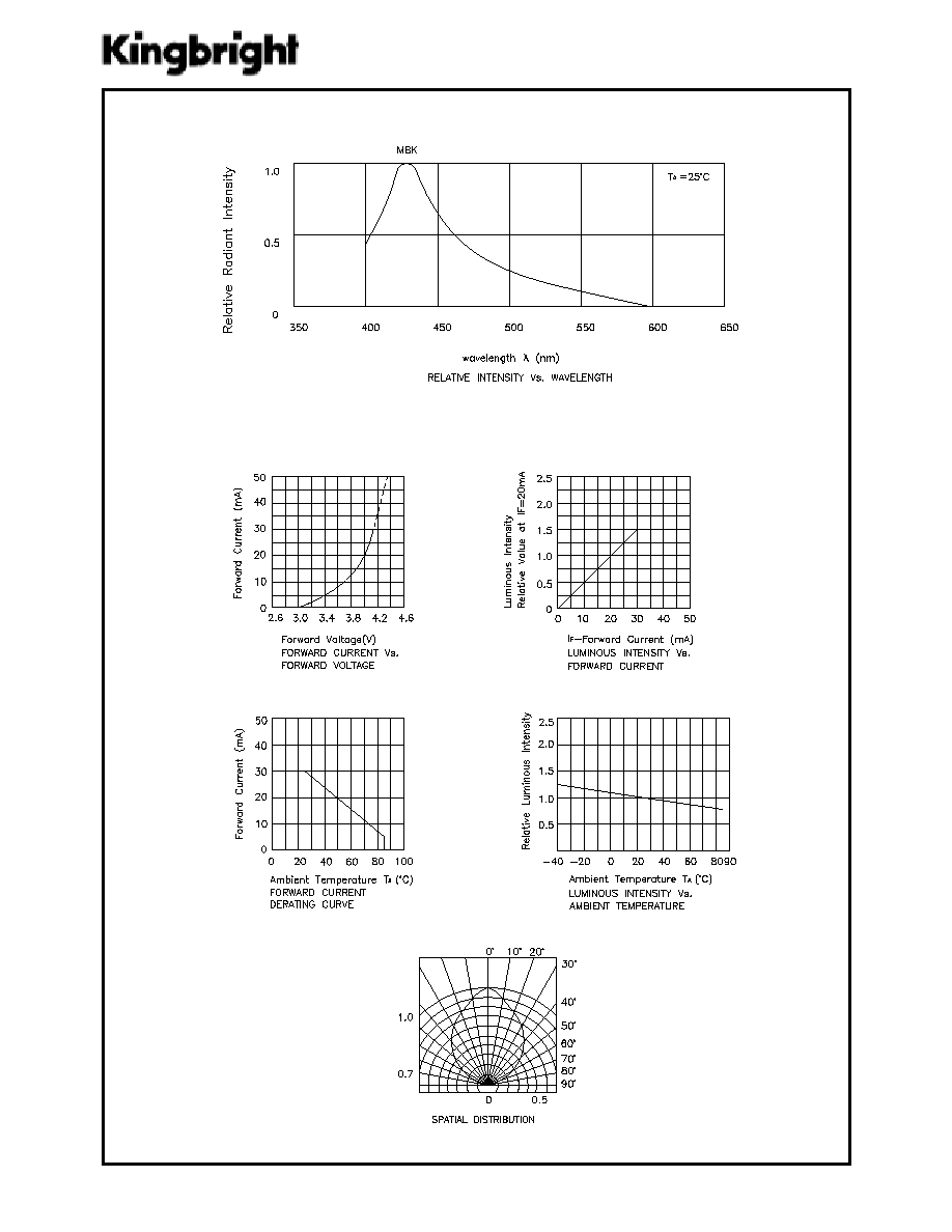
Selection Guide
Note:
1.
1/2 is the angle from optical centerline where the luminous intensity is 1/2 the optical centerline value.
Absolute Maximum Ratings at T
A
=25
∞∞
∞∞
∞
C
Electrical / Optical Characteristics at T
A
=25
∞∞
∞∞
∞
C
Note:
1. 1/10 Duty Cycle, 0.1ms Pulse Width.
.o
N
tra
P
.o
N
tra
P
.o
N
tra
P
.o
N
tra
P
.o
N
tra
P
ec
iD ec
iD ec
iD ec
iD ec
iD
ep
yT
sn
eL
ep
yT
sn
eL
ep
yT
sn
eL
ep
yT
sn
eL
ep
yT
sn
eL
)d
c
m(
vI
)d
c
m(
vI
)d
c
m(
vI
)d
c
m(
vI
)d
c
m(
vI
A
m
02
@
gn
iw
ei
V
gn
iw
ei
V
gn
iw
ei
V
gn
iw
ei
V
gn
iw
ei
V elg
n
A
.ni
M .ni
M .ni
M .ni
M .ni
M
.p
yT .p
yT .p
yT .p
yT .p
yT
2
/
1
2 2
/
1
2 2
/
1
2 2
/
1
2 2
/
1
2
K
C
B
M
02
03
A
A
)N
a
G(
E
U
L
B
R
A
EL
C
R
ET
A
W
6.
2
7
∞0
9
lo
b
m
yS lo
b
m
yS lo
b
m
yS lo
b
m
yS lo
b
m
yS
ret
e
m
ar
a
P
ret
e
m
ar
a
P
ret
e
m
ar
a
P
ret
e
m
ar
a
P
ret
e
m
ar
a
P
ec
iv
e
D ec
iv
e
D ec
iv
e
D ec
iv
e
D ec
iv
e
D
.p
yT .p
yT .p
yT .p
yT .p
yT
.x
a
M .x
a
M .x
a
M .x
a
M .x
a
M
sti
n
U sti
n
U sti
n
U sti
n
U sti
n
U
sn
oit
id
no
C
ts
eT
sn
oit
id
no
C
ts
eT
sn
oit
id
no
C
ts
eT
sn
oit
id
no
C
ts
eT
sn
oit
id
no
C
ts
eT
ka
ep
ht
gn
el
ev
a
W
ka
e
P
eu
lB
03
4
m
n
I
F
A
m
02
=
D
ht
gn
el
ev
a
W
et
an
im
o
D
eu
lB
66
4
m
n
I
F
A
m
02
=
2/
1
ht
di
w-
fla
H
en
iL
lar
tc
ep
S
eu
lB
06
m
n
I
F
A
m
02
=
C
ec
na
tic
ap
a
C
eu
lB
00
1
Fp
V
F
zH
M
1=
f;V
0=
V
F
eg
atl
oV
dr
a
wr
oF
eu
lB
0.
4
5.
4
V
I
F
A
m
02
=
I
R
tn
err
u
C
es
re
ve
R
eu
lB
01
Au
V
R
V5
=
ret
e
m
ar
a
P
ret
e
m
ar
a
P
ret
e
m
ar
a
P
ret
e
m
ar
a
P
ret
e
m
ar
a
P
eu
lB eu
lB eu
lB eu
lB eu
lB
sti
n
U sti
n
U sti
n
U sti
n
U sti
n
U
no
ita
pi
ss
id
re
w
o
P
50
1
W
m
tn
err
u
C
dr
a
wr
oF
C
D
03
A
m
]1[
tn
err
u
C
dr
a
wr
oF
ka
e
P
05
1
A
m
eg
atl
oV
es
re
ve
R
5
V
er
ut
ar
ep
m
eT
eg
ar
ot
S/
gn
ita
re
p
O
04
-
∞
58
+
oT
C
∞
C

SPEC NO: DSAD1222
REV NO: V.1
DATE: MAR/24/2003
PAGE: 4 OF 4
APPROVED: J. Lu
CHECKED: Allen Liu
DRAWN: Z.Y.YANG
Recommended Soldering Pattern
(Units : mm)
Tape Specifications
(Units : mm)
AA3020MBCK
SMT Reflow Soldering Instruction
Number of reflow process shall be less than 2 times and cooling
process to normal temperature is required between first and
second soldering process.