SPEC NO: DSAD0907
REV NO: V.2
DATE:MAY/11/2003
PAGE: 1 OF 6
APPROVED: J.Lu
CHECKED: Allen Liu
DRAWN:D.L.HUANG
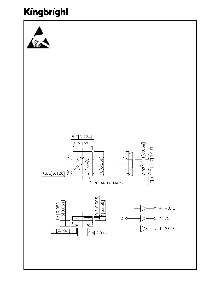
5.0mm X 6.0mm FULL-COLOR SURFACE
MOUNT LED LAMP
Package Dimensions
Features
lCHIPS CAN BE CONTROLLED SEPARATELY.
lSUITABLE FOR ALL SMT ASSEMBLY AND
SOLDER PROCESS.
lAVAILABLE ON TAPE AND REEL.
lPACKAGE: 500PCS / REEL.
Notes:
1. All dimensions are in millimeters (inches).
2. Tolerance is
±
0.25(0.01") unless otherwise noted.
3. Specifications are subject to change without notice.
AAA5060SEEVGPBE
HYPER ORANGE / GREEN / BLUE
Description
The Hyper Orange source color devices are made with
DH InGaAlP on GaAs substrate Light Emitting Diode.
The Green source color devices are made with InGaN
on SiC Light Emitting Diode.
The Blue source color devices are made with InGaN on
SiC Light Emitting Diode.
Static electricity and surge damage the LEDS.
It is recommended to use a wrist band or
anti-electrostatic glove when handling the LEDs.
All devices, equipment and machinery must be
electrically grounded.
ATTENTION
OBSERVE PRECAUTIONS
FOR HANDLING
ELECTROSTATIC
DISCHARGE
SENSITIVE
DEVICES
SPEC NO: DSAD0907
REV NO: V.2
DATE:MAY/11/2003
PAGE: 2 OF 6
APPROVED: J.Lu
CHECKED: Allen Liu
DRAWN:D.L.HUANG
Selection Guide
Electrical / Optical Characteristics at T
A
=25
°°
°°
°
C
Absolute Maximum Ratings at T
A
=25
°°
°°
°
C
.o
N
tra
P
.o
N
tra
P
.o
N
tra
P
.o
N
tra
P
.o
N
tra
P
ec
iD ec
iD ec
iD ec
iD ec
iD
ep
yT
sn
eL
ep
yT
sn
eL
ep
yT
sn
eL
ep
yT
sn
eL
ep
yT
sn
eL
)d
c
m(
vI
)d
c
m(
vI
)d
c
m(
vI
)d
c
m(
vI
)d
c
m(
vI
A
m
03
*
A
m
05
@
gn
iw
ei
V
gn
iw
ei
V
gn
iw
ei
V
gn
iw
ei
V
gn
iw
ei
V elg
n
A
.ni
M .ni
M .ni
M .ni
M .ni
M
.p
yT .p
yT .p
yT .p
yT .p
yT
2
/
1
2 2
/
1
2 2
/
1
2 2
/
1
2 2
/
1
2
E
B
P
G
V
E
E
S0
60
5
A
A
A
)PI
Aa
G
nI(
E
G
N
A
R
O
R
E
PY
H
R
A
EL
C
R
ET
A
W
05
6
00
01
°0
01
)N
a
G
nI(
N
E
E
R
G
08
1*
05
3*
)N
a
G
nI(
E
U
L
B
01
1*
05
2*
lo
b
m
yS lo
b
m
yS lo
b
m
yS lo
b
m
yS lo
b
m
yS
ret
e
m
ar
a
P
ret
e
m
ar
a
P
ret
e
m
ar
a
P
ret
e
m
ar
a
P
ret
e
m
ar
a
P
ec
iv
e
D ec
iv
e
D ec
iv
e
D ec
iv
e
D ec
iv
e
D
.p
yT .p
yT .p
yT .p
yT .p
yT
.x
a
M .x
a
M .x
a
M .x
a
M .x
a
M
sti
n
U sti
n
U sti
n
U sti
n
U sti
n
U
sn
oit
id
no
C
ts
eT
sn
oit
id
no
C
ts
eT
sn
oit
id
no
C
ts
eT
sn
oit
id
no
C
ts
eT
sn
oit
id
no
C
ts
eT
ka
ep
ht
gn
el
ev
a
W
ka
e
P
eg
na
rO
re
py
H nee
rG eul
B
03
6 02
5 56
4
m
n
I
F
A
m
02
=
D
ht
gn
el
ev
a
W
et
an
im
o
D
eg
na
rO
re
py
H nee
rG eul
B
12
6 525
07
4
m
n
I
F
A
m
02
=
2/
1
ht
di
w-
fla
H
en
iL
lar
tc
ep
S
eg
na
rO
re
py
H nee
rG eul
B
02
83
52
m
n
I
F
A
m
02
=
C
ec
na
tic
ap
a
C
eg
na
rO
re
py
H nee
rG eul
B
52
54011
Fp
V
F
zH
M
1=
f;V
0=
V
F
eg
atl
oV
dr
a
wr
oF
eg
na
rO
re
py
H nee
rG eul
B
20.4
7.
3
5.
25.
4 3.
4
V
I
F
A
m
02
=
I
R
tn
err
u
C
es
re
ve
R
llA
01
Au
V
R
V
5
=
Note:
1
.
1/2 is the angle from optical centerline where the luminous intensity is 1/2 the optical centerline value.
2. * Luminous intensity with asterisk is measured at 30mA.
Notes:
1. Within 350mW at all chips are lightened.
2. 1/10 Duty Cycle, 0.1ms Pulse Width.
ret
e
m
ar
a
P
ret
e
m
ar
a
P
ret
e
m
ar
a
P
ret
e
m
ar
a
P
ret
e
m
ar
a
P
eg
na
rO
re
py
H
eg
na
rO
re
py
H
eg
na
rO
re
py
H
eg
na
rO
re
py
H
eg
na
rO
re
py
H
ne
er
G ne
er
G ne
er
G ne
er
G ne
er
G
eu
lB eu
lB eu
lB eu
lB eu
lB
sti
n
U sti
n
U sti
n
U sti
n
U sti
n
U
]1[
tn
oit
ap
iss
id
re
w
o
Pl
at
oT
05
3
W
m
tn
err
u
C
dr
a
wr
oF
C
D
05
03
03
A
m
]2[
tn
err
u
C
dr
a
wr
oF
ka
e
P
59
1
05
1
06
1
A
m
eg
atl
oV
es
re
ve
R
5
V
er
ut
ar
ep
m
eT
eg
ar
ot
S/
gn
ita
re
p
O
04
-
°
58
+
oT
C
°
C
SPEC NO: DSAD0907
REV NO: V.2
DATE:MAY/11/2003
PAGE: 6 OF 6
APPROVED: J.Lu
CHECKED: Allen Liu
DRAWN:D.L.HUANG
AAA5060SEEVGPBE
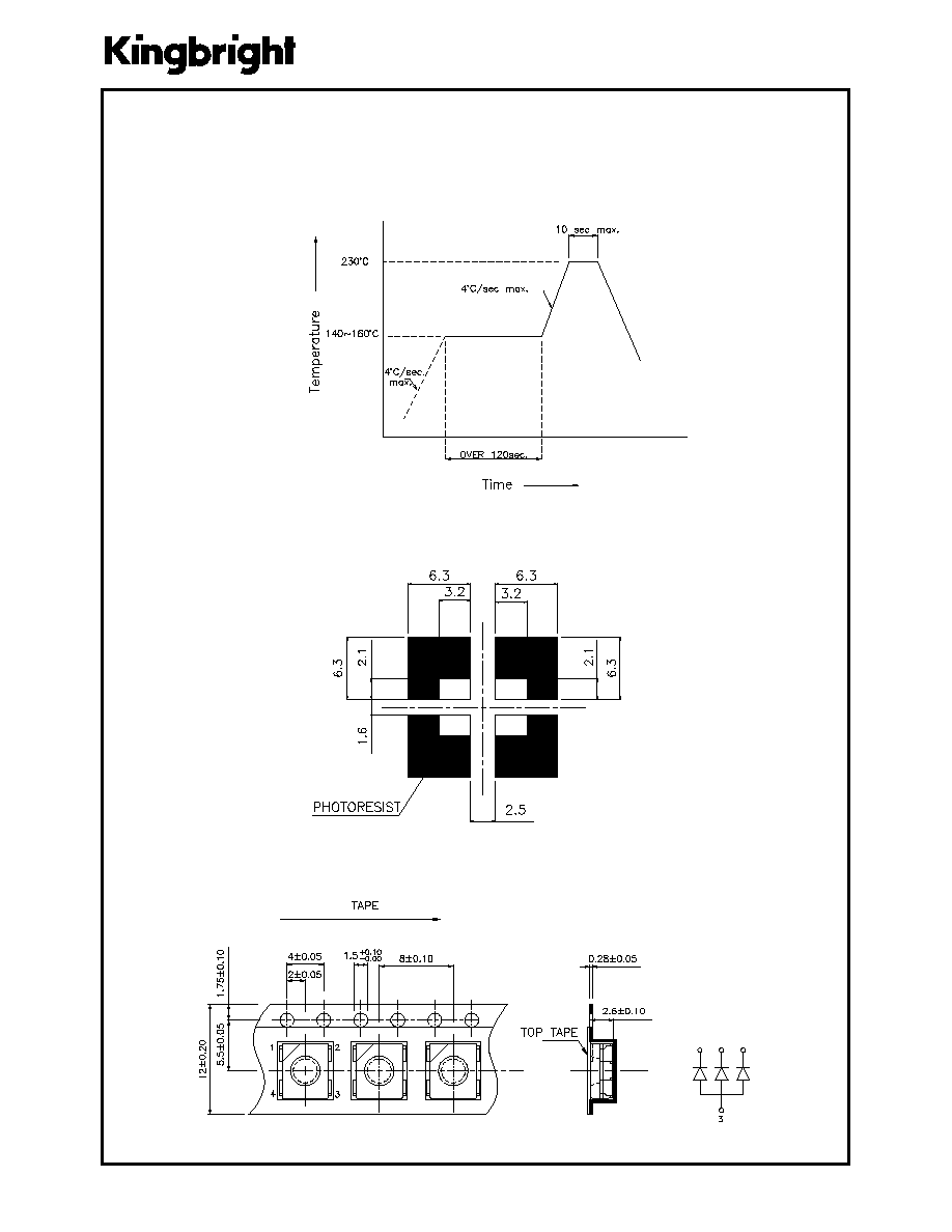
SMT Reflow Soldering Instruction
Number of reflow process shall be less than 2 times and cooling
process to normal temperature is required between first and
second soldering process.
Recommended Soldering Pattern
(Units : mm)
Tape Specifications
(Units : mm)