SPEC NO: DSAB0724
REV NO: V.4
DATE: APR/04/2003
PAGE: 1 OF 4
APPROVED : J. Lu
CHECKED :Allen Liu
DRAWN: X.T.HU
APED3820SRC SUPER BRIGHT RED
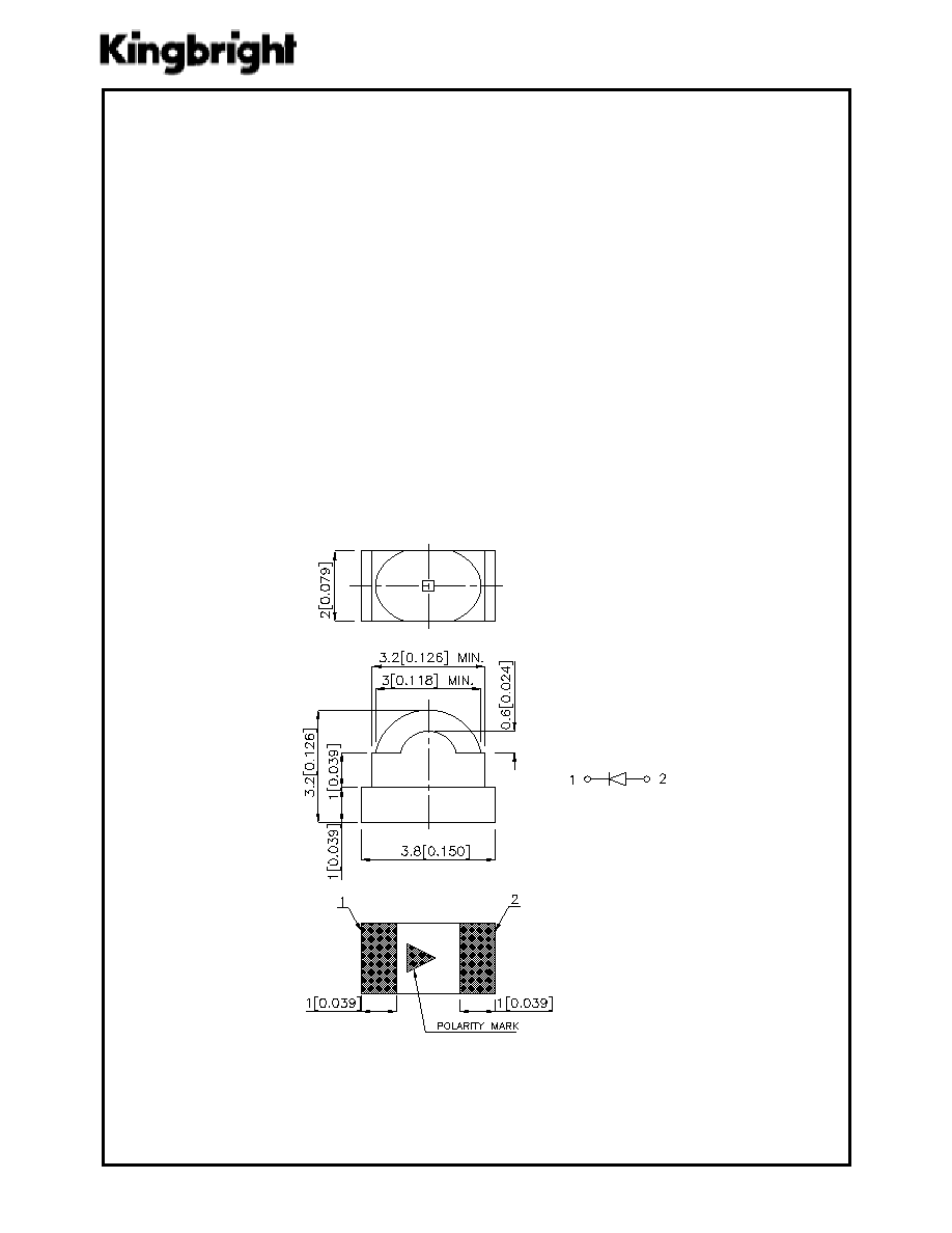
Package Dimensions
Notes:
1. All dimensions are in millimeters (inches).
2. Tolerance is
±
0.2(0.008") unless otherwise noted.
3. Specifications are subject to change without notice.
Features
l
3.8mmx2.0mm SMT LED,3.2mm THICKNESS.
l
LOW POWER CONSUMPTION.
l
IDEAL FOR BACKLIGHT AND INDICATOR.
l
VARIOUS COLORS AND LENS TYPES AVAILABLE.
l
PACKAGE : 500PCS / REEL.
Description
The Super Bright Red source color devices are made
with Gallium Aluminum Arsenide Red Light Emitting
Diode.
3.8x2.0mm DOME LENS SMD CHIP LED LAMP

SPEC NO: DSAB0724
REV NO: V.4
DATE: APR/04/2003
PAGE: 2 OF 4
APPROVED : J. Lu
CHECKED :Allen Liu
DRAWN: X.T.HU
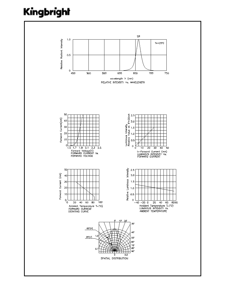
Electrical / Optical Characteristics at T
A
=25
°°
°°
°
C
Absolute Maximum Ratings at T
A
=25
°°
°°
°
C
Note:
1. 1/10 Duty Cycle, 0.1ms Pulse Width.
Selection Guide
Note:
1.
1/2 is the angle from optical centerline where the luminous intensity is 1/2 the optical centerline value.
.o
N
tra
P
.o
N
tra
P
.o
N
tra
P
.o
N
tra
P
.o
N
tra
P
ec
iD ec
iD ec
iD ec
iD ec
iD
ep
yT
sn
eL
ep
yT
sn
eL
ep
yT
sn
eL
ep
yT
sn
eL
ep
yT
sn
eL
)d
c
m(
vI
)d
c
m(
vI
)d
c
m(
vI
)d
c
m(
vI
)d
c
m(
vI
A
m
02
@
gn
iw
ei
V
gn
iw
ei
V
gn
iw
ei
V
gn
iw
ei
V
gn
iw
ei
V elg
n
A
.ni
M .ni
M .ni
M .ni
M .ni
M
.p
yT .p
yT .p
yT .p
yT .p
yT
2
/
1
2 2
/
1
2 2
/
1
2 2
/
1
2 2
/
1
2
C
R
S
02
83
D
E
P
A
)s
AI
A
a
G(
D
E
R
T
H
GI
R
B
R
E
P
U
S
R
A
E
L
C
R
E
T
A
W
01
1
04
2
06
°
)H
(
53
°
)V
(
lo
b
m
yS lo
b
m
yS lo
b
m
yS lo
b
m
yS lo
b
m
yS
ret
e
m
ar
a
P
ret
e
m
ar
a
P
ret
e
m
ar
a
P
ret
e
m
ar
a
P
ret
e
m
ar
a
P
ec
iv
e
D ec
iv
e
D ec
iv
e
D ec
iv
e
D ec
iv
e
D
.p
yT .p
yT .p
yT .p
yT .p
yT
.x
a
M .x
a
M .x
a
M .x
a
M .x
a
M
sti
n
U sti
n
U sti
n
U sti
n
U sti
n
U
sn
oit
id
no
C
ts
eT
sn
oit
id
no
C
ts
eT
sn
oit
id
no
C
ts
eT
sn
oit
id
no
C
ts
eT
sn
oit
id
no
C
ts
eT
ka
ep
ht
gn
el
ev
a
W
ka
e
P
de
R
th
gir
B
re
pu
S
06
6
m
n
I
F
A
m
02
=
D
ht
gn
el
ev
a
W
et
an
im
o
D
de
R
th
gir
B
re
pu
S
04
6
m
n
I
F
A
m
02
=
2/
1
ht
di
w-
fla
H
en
iL
lar
tc
ep
S
de
R
th
gir
B
re
pu
S
02
m
n
I
F
A
m
02
=
C
ec
na
tic
ap
a
C
de
R
th
gir
B
re
pu
S
54
Fp
V
F
zH
M
1=
f;V
0=
V
F
eg
atl
oV
dr
a
wr
oF
de
R
th
gir
B
re
pu
S
58
.1
5.
2
V
I
F
A
m
02
=
I
R
tn
err
u
C
es
re
ve
R
de
R
th
gir
B
re
pu
S
01
Au
V
R
V5
=
ret
e
m
ar
a
P
ret
e
m
ar
a
P
ret
e
m
ar
a
P
ret
e
m
ar
a
P
ret
e
m
ar
a
P
de
R
th
gir
B
re
pu
S
de
R
th
gir
B
re
pu
S
de
R
th
gir
B
re
pu
S
de
R
th
gir
B
re
pu
S
de
R
th
gir
B
re
pu
S
sti
n
U sti
n
U sti
n
U sti
n
U sti
n
U
no
ita
pi
ss
id
re
w
o
P
00
1
W
m
tn
err
u
C
dr
a
wr
oF
C
D
03
A
m
]1[
tn
err
u
C
dr
a
wr
oF
ka
e
P
55
1
A
m
eg
atl
oV
es
re
ve
R
5
V
er
ut
ar
ep
m
eT
eg
ar
ot
S/
gn
ita
re
p
O
04
-
°
58
+
oT
C
°
C

SPEC NO: DSAB0724
REV NO: V.4
DATE: APR/04/2003
PAGE: 4 OF 4
APPROVED : J. Lu
CHECKED :Allen Liu
DRAWN: X.T.HU
Recommended Soldering Pattern
(Units : mm)
Tape Specifications
(Units : mm)
APED3820SRC
SMT Reflow Soldering Instructions
Number of reflow process shall be less than 2 times and cooling
process to normal temperature is required between first and
second soldering process.