 | –≠–ª–µ–∫—Ç—Ä–æ–Ω–Ω—ã–π –∫–æ–º–ø–æ–Ω–µ–Ω—Ç: KB354NT | –°–∫–∞—á–∞—Ç—å:  PDF PDF  ZIP ZIP |

PHOTOCOUPLER
KB354NT
SPEC NO: DSAD2837
REV NO: V.7 DATE: APR/06/2005 PAGE: 1 OF 7
APPROVED: J. Lu
CHECKED: Tracy Deng DRAWN: Y.W.WANG ERP:1205000038
Features
1.AC inputs.
2.High current transfer ratio.
2.Opaque type, mini-flat package.
3.Subminiature type (The volume is smaller than that of our conventional DIP
type by as far as 30%).
4.Isolation voltage between input and output Viso:3750Vrms.
5.Employs double transfer mold technology.
6.Recognized by UL and CUL, file NO.E225308.
7.Packge : 1000Pcs / Reel.
8.RoHS Compliant.
Applications
1.Hybrid substrates that require high density mounting.
2.Programmable controllers.
UNIT : MM[INCH]
TOLERANCE :
±
0.5[
±0
.02] UNLESS OTHERWISE NOTED.
*
*
*
*
PACKAGE DIMENSIONS (UNIT:mm)
SMD Type
PHOTOCOUPLER
KB354NT
SPEC NO: DSAD2837
REV NO: V.7 DATE: APR/06/2005 PAGE: 2 OF 7
APPROVED: J. Lu
CHECKED: Tracy Deng DRAWN: Y.W.WANG ERP:1205000038
*
*
*
*
Absolute Maximum Ratings (Ta=25
∞
∞
∞
∞
C
C
C
C))))
*
*
*
*
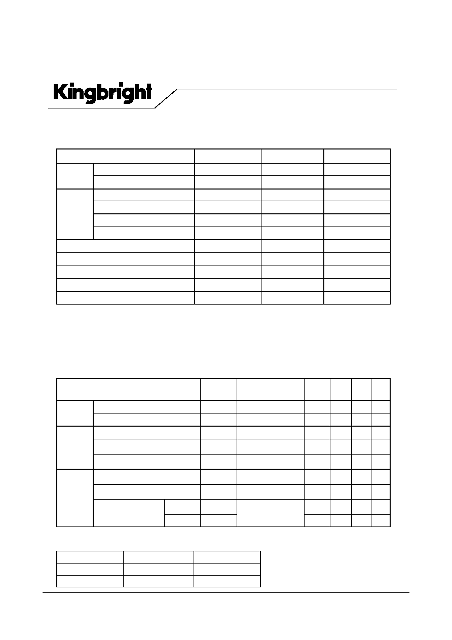
Electro-optical Characteristics
Parameter
Symbol
Conditions
Min.
Typ.
Max.
Unit
Input
Forward voltage
V
F
I
F
=
±
20mA
-
1.2
1.4
V
Peak forward voltage
V
FM
I
FM
=0.5A
-
-
3.0
V
Collector dark current
I
CEO
Vce=20V I
F
=0
-
-
10
-7
A
Collector-emitter breakdown voltage
BV
CEO
I
C
=0.1mA I
F
=0
35
-
-
V
Emitter-collector breakdown voltage
BV
ECO
I
E
=10uA I
F
=0
6
-
V
Transfer
charact-
eristics
Current transfer ration
CTR
I
F
=
±
1mA Vce=5V
20
-
400
Collector-emitter saturation voltage
VCE (sat)
I
F
=
±
20mA IC=1mA
-
0.1
0.2
V
Response
time
Rise time
tr
Vce=2V IC=2mA
RL=100
-
4
18
uS
Fall time
tr
3
18
uS
Output
Parameter
Symbol
Rating
Unit
Input
Forward current
I
F
±
50
mA
Power dissipation
P
70
mW
Output
Collector-emitter voltage
V
CEO
35
V
Emitter-collector voltage
V
ECO
6
V
Collector current
IC
50
mA
Collector power dissipation
P
C
150
mW
Total power dissipation
P tot
170
mW
*1
Isolation voltage
V iso
3750
Vrms
Operating temperature
T opr
-30 to +100
∞
C
Storage temperature
T stg
-55 to +125
∞
C
*2
Soldering temperature
T sol
260
∞
C
*1 40 to 60
RH, AC for1 minute.
*2 For 10 seconds.
Model No.
Rank mark
CTR(%)
KB354N1T
A
50 to 150
KB354NT
A or No mark
20 to 400

PHOTOCOUPLER
KB354NT
SPEC NO: DSAD2837
REV NO: V.7 DATE: APR/06/2005 PAGE: 3 OF 7
APPROVED: J. Lu
CHECKED: Tracy Deng DRAWN: Y.W.WANG ERP:1205000038
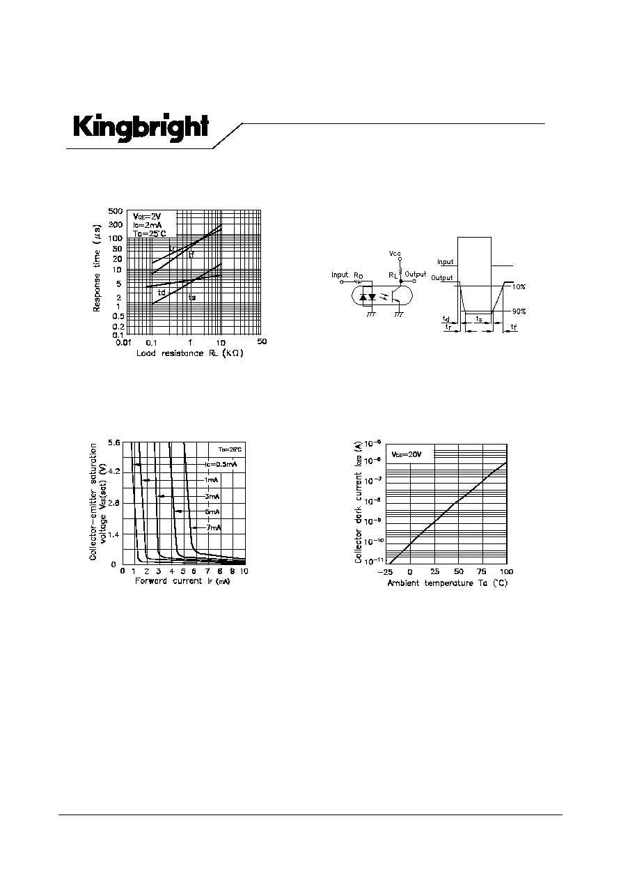
Fig. 1 Current Transfer vs.
Forward Current
Fig. 2 Forward Current vs.
Forward voltage
Fig. 3 Collector Current vs.
Collector-emitter Voltage
Fig. 4 Forward Current vs.
Ambient Temperature
Fig. 5 Collector-emitter Saturation
Voltage vs. Ambient Temperature
PHOTOCOUPLER
KB354NT
SPEC NO: DSAD2837
REV NO: V.7 DATE: APR/06/2005 PAGE: 4 OF 7
APPROVED: J. Lu
CHECKED: Tracy Deng DRAWN: Y.W.WANG ERP:1205000038
Fig. 7 Collector-emitter Saturation
Voltage vs. Forward Current
Fig. 8 Collector Dark Current vs.
Ambient Temperature
Fig. 6 Response Time vs.
Load Resistance
Test Circuit for Response Time

PHOTOCOUPLER
KB354NT
SPEC NO: DSAD2837
REV NO: V.7 DATE: APR/06/2005 PAGE: 5 OF 7
APPROVED: J. Lu
CHECKED: Tracy Deng DRAWN: Y.W.WANG ERP:1205000038
Cycle
One cycle allowed to be dipped in solder including plastic nold portion.
Rosin flux containing small amount of chlorine
(The flux with a maximum chlorine content of 0.2 Wt % is recommended.)
even if the voltage is within the absolute maximum ratings.
Be aware that power is suddenly into the component any surge current may cause damage happen,
2.Cautions regarding noise
Avoid removing the residual flux with freon-based and chlorine-based cleaning solvent.
(2) Cautions
Fluxes
Flux
260
or below (molten solder temperature)
1.Recommended soldering conditions (Dip soldering)
Less than 10 seconds.
Temperature
(1) Dip soldering
Time
* NOTES ON HANDLING
∞
C