
PHOTOCOUPLER
KB817-B
SPEC NO:DSAD1553
REV NO: V.1 DATE:MAY/05/2003 PAGE: 1 OF 8
APPROVED: J.LU
CHECKED: Tracy Deng DRAWN:Y.H.LI
GENERAL PURPOSE
HIGH ISOLATION VOLTAGE
SINGLE TRANSISTOR TYPE
PHOTOCOUPLER SERIES
FEATURES
1.Lead forming (gull wing) type, for surface mounting.
2.High isolation voltage between input and output (Viso=5000 Vrms).
3.Compact dual-in-line package
KB817-B:1-channel type
4.Recognized by UL and CUL,file NO.E225308.
DESCRIPTION
1.The KB817-B (1-channel) is optically coupled isolators containing a GaAS light emitting
diode and an NPN silicon phototransistor.
2.The lead pitch is 2.54mm.
3.Solid insulation thickness between emitting diode and output phototransistor:>=0.6mm.
APPLICATIONS
1.Computer terminals.
2.Registers,copiers,automatic vending machines.
3.System appliances,measuring instruments.
4.Programmable logic controller.
5.Signal transmission between circuits of different potentials and impedances.
PHOTOCOUPLER
KB817-B
SPEC NO:DSAD1553
REV NO: V.1 DATE:MAY/05/2003 PAGE: 2 OF 8
APPROVED: J.LU
CHECKED: Tracy Deng DRAWN:Y.H.LI
*
Absolute Maximum Ratings (T
=
=25
��
��
�
C)
*1
40 to 60% RH,AC for 1 minute.
*2
For 10 seconds.
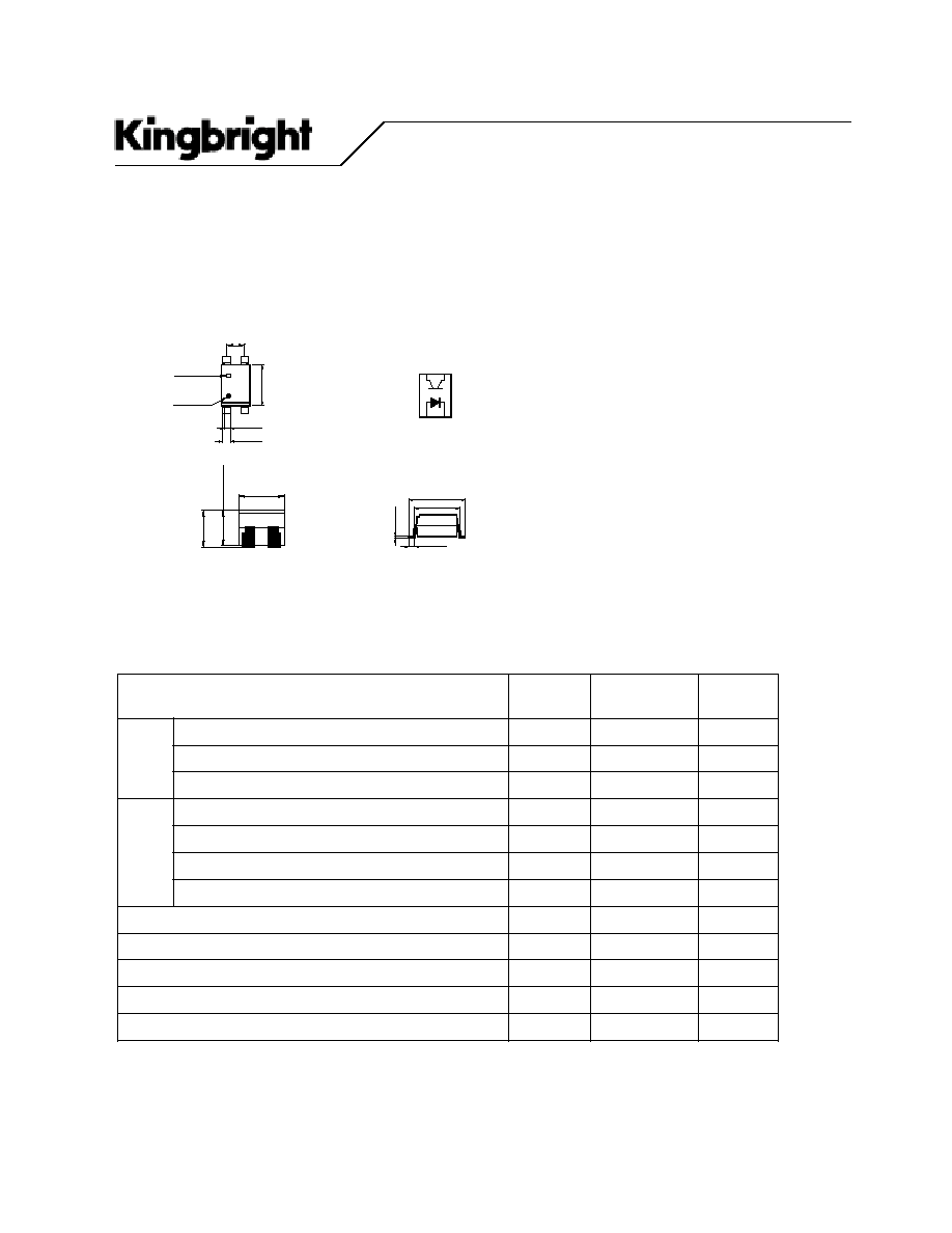
1.20[0.047]�0.3
Cathode
1. Anode 2.
4.
Emitter
3.
Collector
4.58[0.18]
3
.
50
[
0
.
1
38
]
3.7
[
0.146
]
0.
25[
0.
01
]
7.20[0.2835]
0.96[0.038]
10.0[.3935] +0.0
-0.5
Internal connection
diagram
KB817-B
0.90[0.035]�0.2
K
B
817-B
6.
50[
0.
25
6]
rank mark
mark
1
2
Anode
CTR
2.54[0.1]�0.25
4
3
Top View
3
4
1 2
1.25[0495]
*PACKAGE DIMENSIONS (UNIT:mm)
Lead Bending Type
TOLERANCE
: �
: �
: �
: �
: �
0.5[
�
�
�
�
�
0.02] UNLESS OTHERWISE NOTED.
.
.
. .
r
e
t
e
m
a
r
a
P
r
e
t
e
m
a
r
a
P
r
e
t
e
m
a
r
a
P
r
e
t
e
m
a
r
a
P
r
e
t
e
m
a
r
a
P
l
o
b
m
y
S
l
o
b
m
y
S
l
o
b
m
y
S
l
o
b
m
y
S
l
o
b
m
y
S
g
n
it
a
R
g
n
it
a
R
g
n
it
a
R
g
n
it
a
R
g
n
it
a
R
ti
n
U ti
n
U ti
n
U ti
n
U ti
n
U
t
u
p
n
I
t
n
e
r
r
u
c
d
r
a
w
r
o
F
I
F
0
5
A
m
e
g
a
tl
o
v
e
s
r
e
v
e
R
V
R
6
V
n
o
it
a
p
i
s
s
i
d
r
e
w
o
P
P
0
7
W
m
t
u
p
t
u
O
e
g
a
tl
o
v
r
e
tt
i
m
e
-
r
o
t
c
e
ll
o
C
V
O
E
C
5
3
V
e
g
a
tl
o
v
r
o
t
c
e
ll
o
c
-
r
e
tt
i
m
E
V
O
C
E
6
V
t
n
e
r
r
u
c
r
o
t
c
e
ll
o
C
I
C
0
5
A
m
n
o
it
a
p
i
s
s
i
d
r
e
w
o
p
r
o
t
c
e
ll
o
C
P
C
0
5
1
W
m
n
o
it
a
p
i
s
s
i
d
r
e
w
o
p
l
a
t
o
T
t
o
t
P
0
0
2
W
m
1
*
e
g
a
tl
o
v
n
o
it
a
l
o
s
I
o
s
i
V
0
0
0
5
s
m
r
V
e
r
u
t
a
r
e
p
m
e
t
g
n
it
a
r
e
p
O
r
p
o
T
0
0
1
+
~
0
3
-
�
C
e
r
u
t
a
r
e
p
m
e
t
e
g
a
r
o
t
S
g
t
s
T
5
2
1
+
~
5
5
-
�
C
2
*
e
r
u
t
a
r
e
p
m
e
t
g
n
ir
e
d
l
o
S
l
o
s
T
0
6
2
�
C
PHOTOCOUPLER
KB817-B
SPEC NO:DSAD1553
REV NO: V.1 DATE:MAY/05/2003 PAGE: 3 OF 8
APPROVED: J.LU
CHECKED: Tracy Deng DRAWN:Y.H.LI
X 100%
Classification table of current transfer ratio is shown below.
CTR=
F
I
Ic
*Electro-optical Characteristics
.
o
N
l
e
d
o
M
.
o
N
l
e
d
o
M
.
o
N
l
e
d
o
M
.
o
N
l
e
d
o
M
.
o
N
l
e
d
o
M
k
r
a
m
k
n
a
R
k
r
a
m
k
n
a
R
k
r
a
m
k
n
a
R
k
r
a
m
k
n
a
R
k
r
a
m
k
n
a
R
)
%
(
R
T
C
)
%
(
R
T
C
)
%
(
R
T
C
)
%
(
R
T
C
)
%
(
R
T
C
B
-
L
7
1
8
B
K
L
0
0
1
o
t
0
5
B
-
A
7
1
8
B
K
A
0
6
1
o
t
0
8
B
-
B
7
1
8
B
K
B
0
6
2
o
t
0
3
1
B
-
C
7
1
8
B
K
C
0
0
4
o
t
0
0
2
B
-
D
7
1
8
B
K
D
0
0
6
o
t
0
0
3
B
-
B
A
7
1
8
B
K
B
r
o
A
0
6
2
o
t
0
8
B
-
C
B
7
1
8
B
K
C
r
o
B
0
0
4
o
t
0
3
1
B
-
D
C
7
1
8
B
K
D
r
o
C
0
0
6
o
t
0
0
2
B
-
C
A
7
1
8
B
K
C
r
o
B
,
A
0
0
4
o
t
0
8
B
-
D
B
7
1
8
B
K
D
r
o
C
,
B
0
0
6
o
t
0
3
1
B
-
D
A
7
1
8
B
K
D
r
o
C
,
B
,
A
0
0
6
o
t
0
8
B
-
7
1
8
B
K
k
r
a
m
o
N
r
o
D
,
C
,
B
,
A
,
L
0
0
6
o
t
0
5
r
e
t
e
m
a
r
a
P
r
e
t
e
m
a
r
a
P
r
e
t
e
m
a
r
a
P
r
e
t
e
m
a
r
a
P
r
e
t
e
m
a
r
a
P
l
o
b
m
y
S
l
o
b
m
y
S
l
o
b
m
y
S
l
o
b
m
y
S
l
o
b
m
y
S
s
n
o
it
i
d
n
o
C
s
n
o
it
i
d
n
o
C
s
n
o
it
i
d
n
o
C
s
n
o
it
i
d
n
o
C
s
n
o
it
i
d
n
o
C
.
n
i
M .
n
i
M .
n
i
M .
n
i
M .
n
i
M
.
p
y
T .
p
y
T .
p
y
T .
p
y
T .
p
y
T
.
x
a
M .
x
a
M .
x
a
M .
x
a
M .
x
a
M
ti
n
U ti
n
U ti
n
U ti
n
U ti
n
U
t
u
p
n
I
e
g
a
tl
o
v
d
r
a
w
r
o
F
V
F
I
F
A
m
0
2
=
_
_
_
2
.
1
4
.
1
V
e
g
a
tl
o
v
d
r
a
w
r
o
f
k
a
e
P
V
M
F
I
M
F
A
5
.
0
=
_
_
_
_
_
_
0
.
3
V
t
n
e
r
r
u
c
e
s
r
e
v
e
R
I
R
V
R
V
4
=
_
_
_
_
_
_
0
1
�
A
t
u
p
t
u
O
t
n
e
r
r
u
c
k
r
a
d
r
o
t
c
e
ll
o
C
I
O
E
C
V
E
C
,
V
0
2
=
I
F
A
m
0
=
_
_
_
_
_
_
0
1
7
-
A
n
r
e
f
s
n
a
r
T
-t
c
a
r
a
h
c
s
c
it
s
ir
e
1
*
o
it
a
r
r
e
f
s
n
a
rt
t
n
e
r
r
u
C
R
T
C
I
F
V
,
A
m
5
=
E
C
V
5
=
0
5
_
_
_
0
0
6
%
e
g
a
tl
o
v
n
o
it
a
r
u
t
a
s
r
e
tt
i
m
e
-
r
o
t
c
e
ll
o
C
V
(
E
C
t
a
s
)
I
F
,
A
m
0
2
=
I
C
A
m
1
=
_
_
_
1
.
0
2
.
0
8
y
c
n
e
u
q
e
r
f
ff
o
-
t
u
C
f
c
V
E
C
,
V
5
=
I
C
A
m
2
=
R
L
0
0
1
=
,
B
d
3
-
_
_
_
0
8
_
_
_
z
H
K
e
m
it
e
s
n
o
p
s
e
R
e
m
it
e
s
i
R
t
r
V
E
C
I
,
V
2
=
C
A
m
2
=
R
L
0
0
1
=
_
_
_
4
8
1
�
s
e
m
it
ll
a
F
t
f
_
_
_
3
8
1
�
s
PHOTOCOUPLER
KB817-B
SPEC NO:DSAD1553
REV NO: V.1 DATE:MAY/05/2003 PAGE: 4 OF 8
APPROVED: J.LU
CHECKED: Tracy Deng DRAWN:Y.H.LI
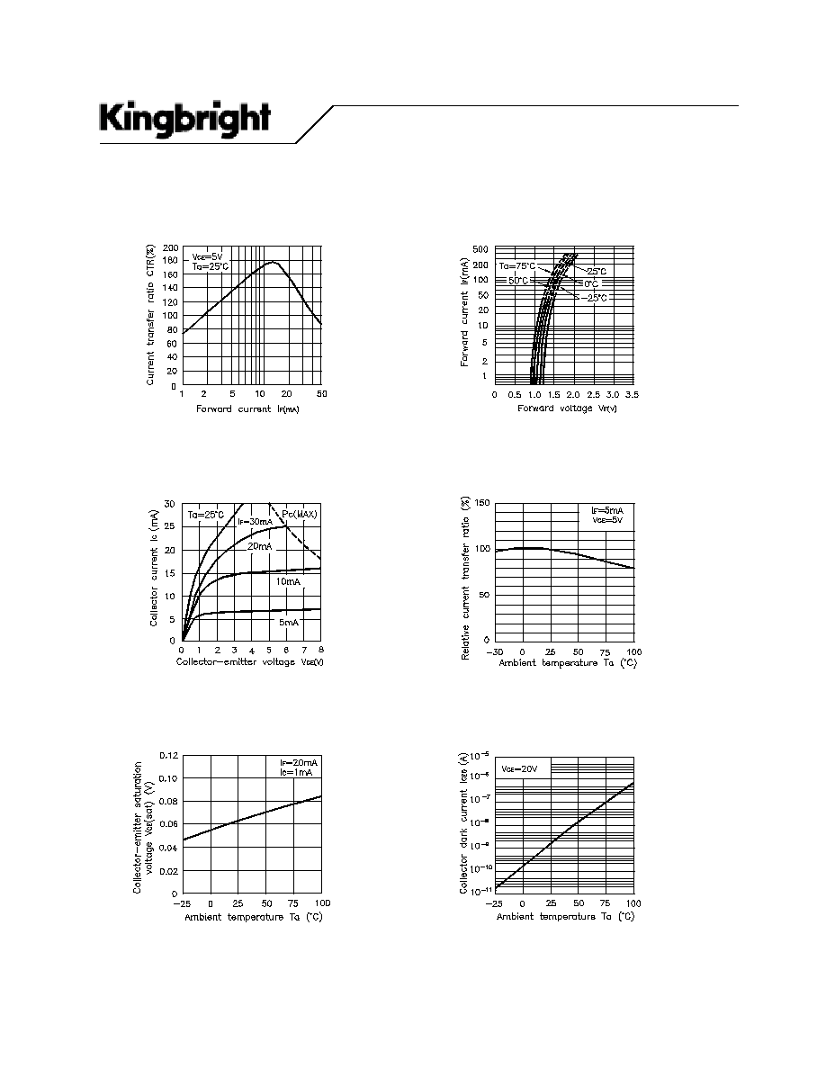
Fig. 3 Collector Current vs.
Collector-emitter Voltage
Fig. 4 Relative Current Transfer Ratio
vs. Ambient Temperature
Fig. 1 Current Transfer Ratio vs.
Forward Current
Fig. 2 Forward Current vs.
Forward voltage
Fig. 5 Collector-emitter Saturation
Voltage vs. Ambient Temperature
Fig. 6 Collector Dark Current vs.
Ambient Temperature

PHOTOCOUPLER
KB817-B
SPEC NO:DSAD1553
REV NO: V.1 DATE:MAY/05/2003 PAGE: 5 OF 8
APPROVED: J.LU
CHECKED: Tracy Deng DRAWN:Y.H.LI
g
[
Fig. 10 Frequency Response
Test Circuit for Frequency Response
[
[
[
Fig. 9 Response Time vs.
Load Resistance
Fig. 7 Forward Current vs.
Ambient Temperature
Fig. 8 Collector Power Dissipation vs.
Ambient Temperature
Test Circuit for Response Time