/home/web/doc/html/kingbright/175885

PHOTOCOUPLER
KB836
SPEC NO: DSAD1547
REV NO: V.1
DATE: APR/28/2003 PAGE: 1 OF 8
APPROVED: J.LU
CHECKED: Tracy Deng
DRAWN: Z.Y.YANG
2.Registers, copiers, automatic vending machines
3.System appliances, measuring instruments
a GaAS light emitting diode and an NPN silicon phototransistor.
5.Signal transmission between circuits of different potentials and impedances
3.Solid insulation thickness between emitting diode and output phototransistor: >= 0.6mm.
4.Programmable logic controller
APPLICATIONS
1.Computer terminals
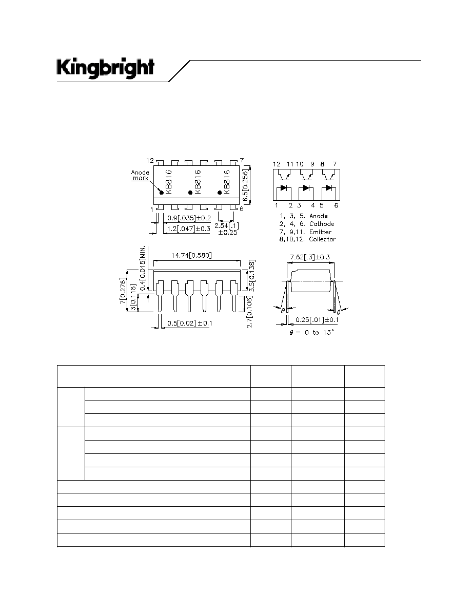
2.The lead pitch is 2.54mm
HIGH COLLECTOR VOLTAGE
1.High isolation voltage between input and output (Viso=5000
Vrms)
4.Recognized by UL and CUL, file NO. E225308
3.Compact dual-in-line package
DESCRIPTION
2.High Collector-emitter voltage (Vceo=70 V)
FEATURES
PHOTOCOUPLER SERIES
SINGLE TRANSISTOR TYPE
HIGH ISOLATION VOLTAGE
GENERAL PURPOSE
1.The KB836 (3-channel) is optically coupled isolators containing
KB836:3-channel type
PHOTOCOUPLER
KB836
SPEC NO: DSAD1547
REV NO: V.1
DATE: APR/28/2003 PAGE: 2 OF 8
APPROVED: J.LU
CHECKED: Tracy Deng
DRAWN: Z.Y.YANG
* PACKAGE DIMENSIONS (UNIT: mm)
TOLERANCE :
��
��
�
0.5[
��
��
�
0.02 ] UNLESS OTHERWISE NOTED.
*
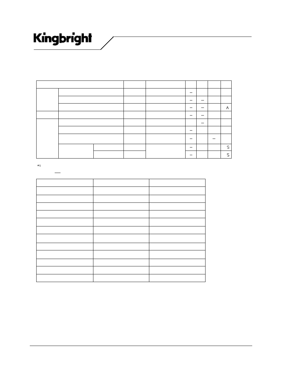
Absolute Maximum Ratings (T
=
=25
��
��
�
C)
*1
40 to 60% RH,AC for 1 minute.
*2
For 10 seconds.
r
e
t
e
m
a
r
a
P
r
e
t
e
m
a
r
a
P
r
e
t
e
m
a
r
a
P
r
e
t
e
m
a
r
a
P
r
e
t
e
m
a
r
a
P
l
o
b
m
y
S
l
o
b
m
y
S
l
o
b
m
y
S
l
o
b
m
y
S
l
o
b
m
y
S
g
n
it
a
R
g
n
it
a
R
g
n
it
a
R
g
n
it
a
R
g
n
it
a
R
ti
n
U ti
n
U ti
n
U ti
n
U ti
n
U
t
u
p
n
I
t
n
e
r
r
u
c
d
r
a
w
r
o
F
I
F
0
5
A
m
e
g
a
tl
o
v
e
s
r
e
v
e
R
V
R
6
V
n
o
it
a
p
i
s
s
i
d
r
e
w
o
P
P
0
7
W
m
t
u
p
t
u
O
e
g
a
tl
o
v
r
e
tt
i
m
e
-
r
o
t
c
e
ll
o
C
V
O
E
C
0
7
V
e
g
a
tl
o
v
r
o
t
c
e
ll
o
c
-
r
e
tt
i
m
E
V
O
C
E
6
V
t
n
e
r
r
u
c
r
o
t
c
e
ll
o
C
I
C
0
5
A
m
n
o
it
a
p
i
s
s
i
d
r
e
w
o
p
r
o
t
c
e
ll
o
C
P
C
0
5
1
W
m
n
o
it
a
p
i
s
s
i
d
r
e
w
o
p
l
a
t
o
T
t
o
t
P
0
0
2
W
m
1
*
e
g
a
tl
o
v
n
o
it
a
l
o
s
I
o
s
i
V
0
0
0
5
s
m
r
V
e
r
u
t
a
r
e
p
m
e
t
g
n
it
a
r
e
p
O
r
p
o
T
0
0
1
+
~
0
3
-
�
C
e
r
u
t
a
r
e
p
m
e
t
e
g
a
r
o
t
S
g
t
s
T
5
2
1
+
~
5
5
-
�
C
2
*
e
r
u
t
a
r
e
p
m
e
t
g
n
ir
e
d
l
o
S
l
o
s
T
0
6
2
�
C
PHOTOCOUPLER
KB836
SPEC NO: DSAD1547
REV NO: V.1
DATE: APR/28/2003 PAGE: 3 OF 8
APPROVED: J.LU
CHECKED: Tracy Deng
DRAWN: Z.Y.YANG
V
CE
=2V, I
C
=2mA
R
L
=100
[
Response time
X 100%
Classification table of current transfer ratio is shown below.
CTR=
.
I
Ic
Fall time
f
t
Cut-off frequency
Transfer
charact-
eristics
Rise time
V
CE
=5V, I
C
=2mA
R
L
=100
[, -3dB
c
r
f
t
* Electro-optical Characteristics
*1
Collector-emitter saturation voltage
Collector dark current
Peak forward voltage
Current transfer ratio
Reverse current
Forward voltage
Output
Input
I
F
=20mA
V
F
CTR
V
CE(
sat
)
50
I
F
=5mA, V
CE
=5V
I
F
=20mA, I
C
=1mA
V
CE
=20V,I
F
=0mA
V
R
=4V
I
FM
=0.5A
I
R
I
CEO
V
FM
Symbol
Parameter
Conditions
Min.
18
3
C
V
1.4
1.2
%
600
kH
z
18
80
4
C
0.2
0.1
V
C
10
10
A
-7
3.0
V
Max.
Typ.
Unit
Model No.
KB836B
KB836A
KB836C
KB836AB
KB836D
KB836CD
KB836BC
KB836
KB836AC
KB836BD
KB836AD
KB836L
B,C or D
130 to 600
A,B,C or D
50 to 600
80 to 600
C or D
A,B or C
B or C
A or B
Rank mark
B
D
C
A
L
130 to 260
80 to 400
200 to 600
130 to 400
300 to 600
80 to 260
200 to 400
50 to 100
80 to 160
CTR (%)
L,A,B,C,D or No mark
(T
=
=25
�
C)
PHOTOCOUPLER
KB836
SPEC NO: DSAD1547
REV NO: V.1
DATE: APR/28/2003 PAGE: 4 OF 8
APPROVED: J.LU
CHECKED: Tracy Deng
DRAWN: Z.Y.YANG
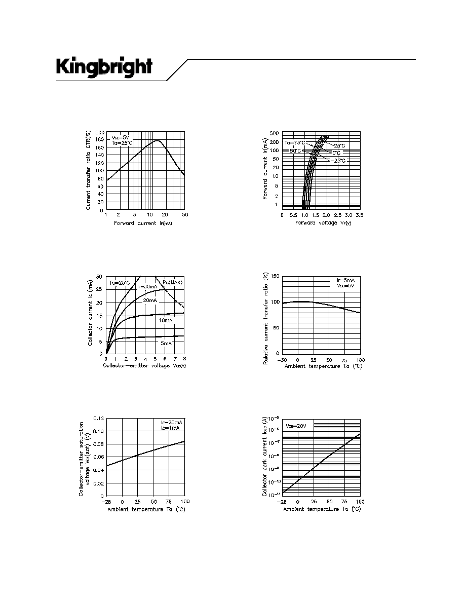
Fig. 3 Collector Current vs.
Collector-emitter Voltage
Fig. 4 Relative Current Transfer Ratio
vs. Ambient Temperature
Fig. 1 Current Transfer Ratio vs.
Forward Current
Fig. 2 Forward Current vs.
Forward voltage
Fig. 5 Collector-emitter Saturation
Voltage vs. Ambient Temperature
Fig. 6 Collector Dark Current vs.
Ambient Temperature
PHOTOCOUPLER
KB836
SPEC NO: DSAD1547
REV NO: V.1
DATE: APR/28/2003 PAGE: 5 OF 8
APPROVED: J.LU
CHECKED: Tracy Deng
DRAWN: Z.Y.YANG
g
[
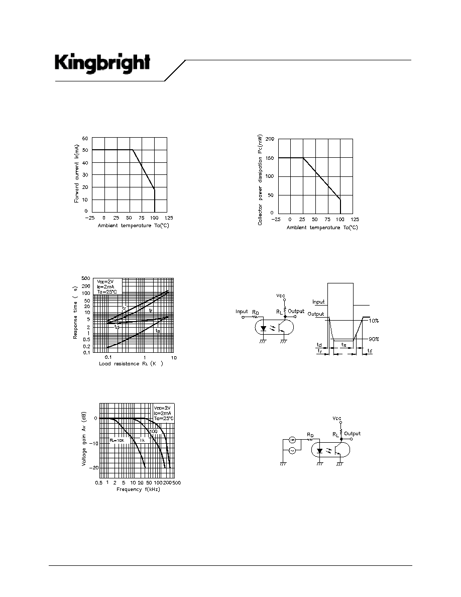
Fig. 10 Frequency Response
Test Circuit for Frequency Response
[
[
[
Fig. 9 Response Time vs.
Load Resistance
Fig. 7 Forward Current vs.
Ambient Temperature
Fig. 8 Collector Power Dissipation vs.
Ambient Temperature
Test Circuit for Response Time