SPEC NO: KDA0431
REV NO: V.1
DATE: SEP/21/2001
PAGE: 1 OF 5
APPROVED: J.LU
CHECKED:
DRAWN: J.X.FU
KP-3216F3C
KP-3216SF4C
INFRA-RED EMITTING DIODES
Features
!
!
!
!
!
WATER CLEAR LENS AVAILABLE.
!
!
!
!
!
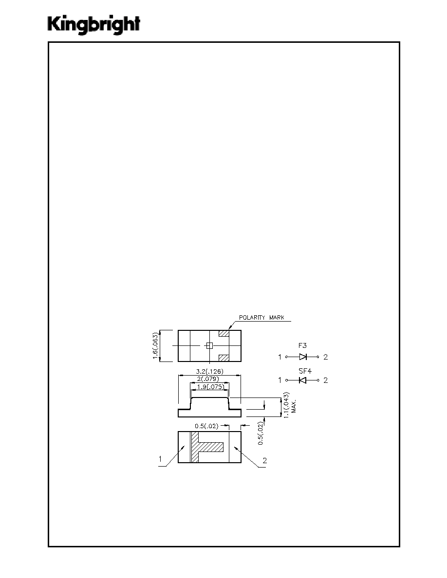
3.2mmx1.6mm SMT LED, 1.1mm THICKNESS.
!
!
!
!
!
HIGH POWER OUTPUT.
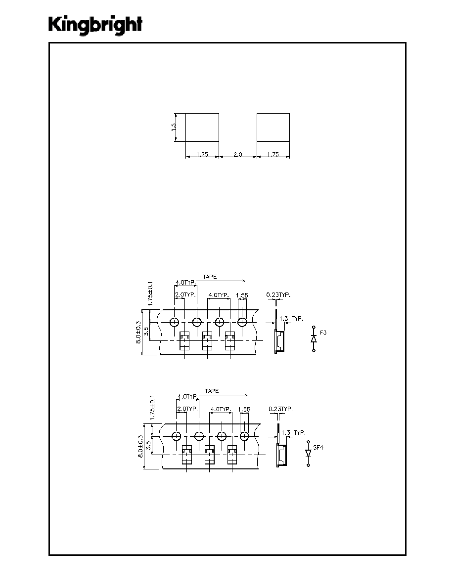
Package Dimensions
Notes:
1. All dimensions are in millimeters (inches).
2. Tolerance is
±
0.2(0.0079") unless otherwise noted.
3. Lead spacing is measured where the lead emerge package.
4. Specifications are subject to change without notice.
Description
F3 Made with Gallium Arsenide Infrared Emitting diodes.
SF4 Made with Gallium Aluminum Arsenide Infrared
Emitting diodes.
!
!
!
!
!
PACKAGE: 2000PCS/REEL.
SPEC NO: KDA0431
REV NO: V.1
DATE: SEP/21/2001
PAGE: 2 OF 5
APPROVED: J.LU
CHECKED:
DRAWN: J.X.FU
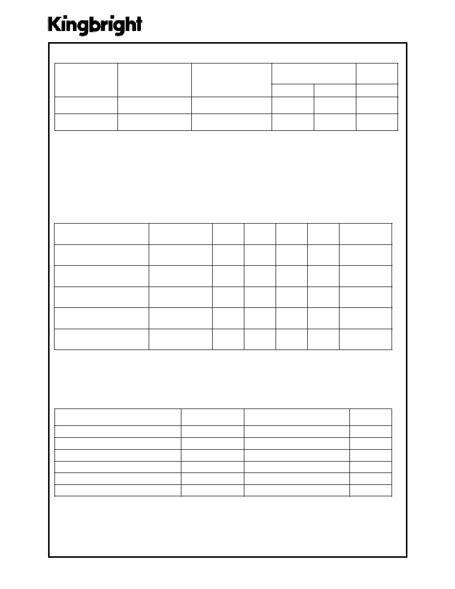
Electrical / Optical Characteristics at T
)
=25
°°
°°
°
C
Absolute Maximum Ratings at T
)
=25
°°
°°
°
C
m
e
tI m
e
tI m
e
tI m
e
tI m
e
tI
l
o
b
m
y
S
l
o
b
m
y
S
l
o
b
m
y
S
l
o
b
m
y
S
l
o
b
m
y
S
4
F
S
&
3
F
4
F
S
&
3
F
4
F
S
&
3
F
4
F
S
&
3
F
4
F
S
&
3
F
s
ti
n
U s
ti
n
U s
ti
n
U s
ti
n
U s
ti
n
U
n
o
it
a
p
i
s
s
i
D
r
e
w
o
P
P
T
0
0
1
W
m
t
n
e
r
r
u
C
d
r
a
w
r
o
F
I
F
0
5
A
m
]
1
[t
n
e
r
r
u
C
d
r
a
w
r
o
F
k
a
e
P
i
S
F
2
.
1
A
e
g
a
tl
o
V
e
s
r
e
v
e
R
V
R
5
V
e
r
u
t
a
r
e
p
m
e
T
g
n
it
a
r
e
p
O
T
A
5
8
+
~
0
4
-
°
C
e
r
u
t
a
r
e
p
m
e
T
e
g
a
r
o
t
S
T
G
T
S
5
8
+
~
0
4
-
°
C
Note:
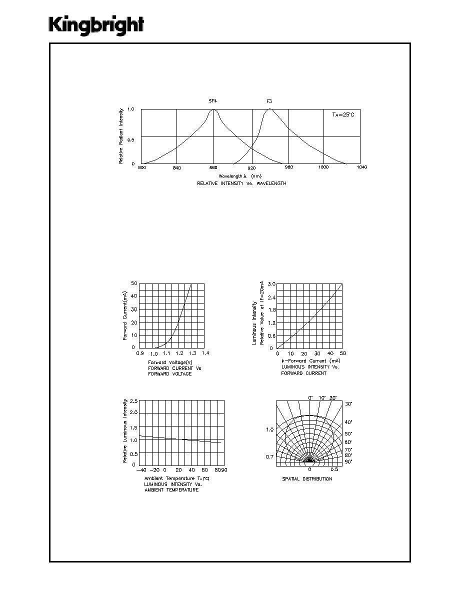
1.1/100 Duty Cycle, 10us Pluse Width.
Selection Guide
.
o
N
t
r
a
P
.
o
N
t
r
a
P
.
o
N
t
r
a
P
.
o
N
t
r
a
P
.
o
N
t
r
a
P
e
c
i
D e
c
i
D e
c
i
D e
c
i
D e
c
i
D
e
p
y
T
s
n
e
L
e
p
y
T
s
n
e
L
e
p
y
T
s
n
e
L
e
p
y
T
s
n
e
L
e
p
y
T
s
n
e
L
)
r
s
/
W
m
(
=
o
P
)
r
s
/
W
m
(
=
o
P
)
r
s
/
W
m
(
=
o
P
)
r
s
/
W
m
(
=
o
P
)
r
s
/
W
m
(
=
o
P
A
m
0
2
@
g
n
i
w
e
i
V
g
n
i
w
e
i
V
g
n
i
w
e
i
V
g
n
i
w
e
i
V
g
n
i
w
e
i
V
e
l
g
n
A
.
n
i
M .
n
i
M .
n
i
M .
n
i
M .
n
i
M
.
p
y
T .
p
y
T .
p
y
T .
p
y
T .
p
y
T
2
/
1
2 2
/
1
2 2
/
1
2 2
/
1
2 2
/
1
2
C
3
F
6
1
2
3
-
P
K
s
A
a
G
R
A
E
L
C
R
E
T
A
W
5
.
0
2
.
1
°
0
2
1
C
4
F
S
6
1
2
3
-
P
K
s
A
l
A
a
G
R
A
E
L
C
R
E
T
A
W
5
.
0
1
°
0
2
1
Note:
1.
1/2 is the angle from optical centerline where the luminous intensity is 1/2 the optical centerline value.
m
e
tI m
e
tI m
e
tI m
e
tI m
e
tI
N
/
P N
/
P N
/
P N
/
P N
/
P
l
o
b
m
y
S
l
o
b
m
y
S
l
o
b
m
y
S
l
o
b
m
y
S
l
o
b
m
y
S
.
p
y
T .
p
y
T .
p
y
T .
p
y
T .
p
y
T
.
x
a
M .
x
a
M .
x
a
M .
x
a
M .
x
a
M
ti
n
U ti
n
U ti
n
U ti
n
U ti
n
U
n
o
it
i
d
n
o
C
n
o
it
i
d
n
o
C
n
o
it
i
d
n
o
C
n
o
it
i
d
n
o
C
n
o
it
i
d
n
o
C
e
g
a
tl
o
V
d
r
a
w
r
o
F
3
F
4
F
S
V
F
2
.
1
3
.
1
5
.
1
7
.
1
V
A
m
0
2
=
F
I
t
n
e
r
r
u
C
e
s
r
e
v
e
R
3
F
4
F
S
I
R
-
0
1
0
1
A
u
V
5
=
R
V
e
c
n
a
ti
c
a
p
a
C
3
F
4
F
S
C
0
9
0
9
-
F
p
z
H
M
1
=
f
,
V
0
=
F
V
h
t
g
n
e
l
e
v
a
W
l
a
rt
c
e
p
S
k
a
e
P
3
F
4
F
S
P
0
4
9
0
8
8
-
m
n
A
m
0
2
=
F
I
h
t
d
i
w
d
n
a
B
l
a
rt
c
e
p
S
3
F
4
F
S
0
5
0
5
-
m
n
A
m
0
2
=
F
I
SPEC NO: KDA0431
REV NO: V.1
DATE: SEP/21/2001
PAGE: 4 OF 5
APPROVED: J.LU
CHECKED:
DRAWN: J.X.FU
KP-3216F3C,KP-3216SF4C
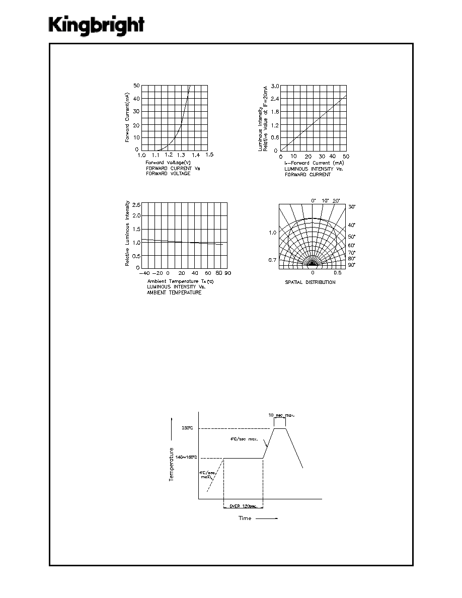
SMT Reflow Soldering Instructions
Number of reflow process shall be less than 2 times and
cooling process to normal temperature is required between
first and second soldering process.
KP-3216SF4C