SPEC NO: CDA0659
REV NO: V.1
DATE: OCT/30/2001
PAGE: 1 OF3
APPROVED: J.Lu
CHECKED :
DRAWN: X.H.FU
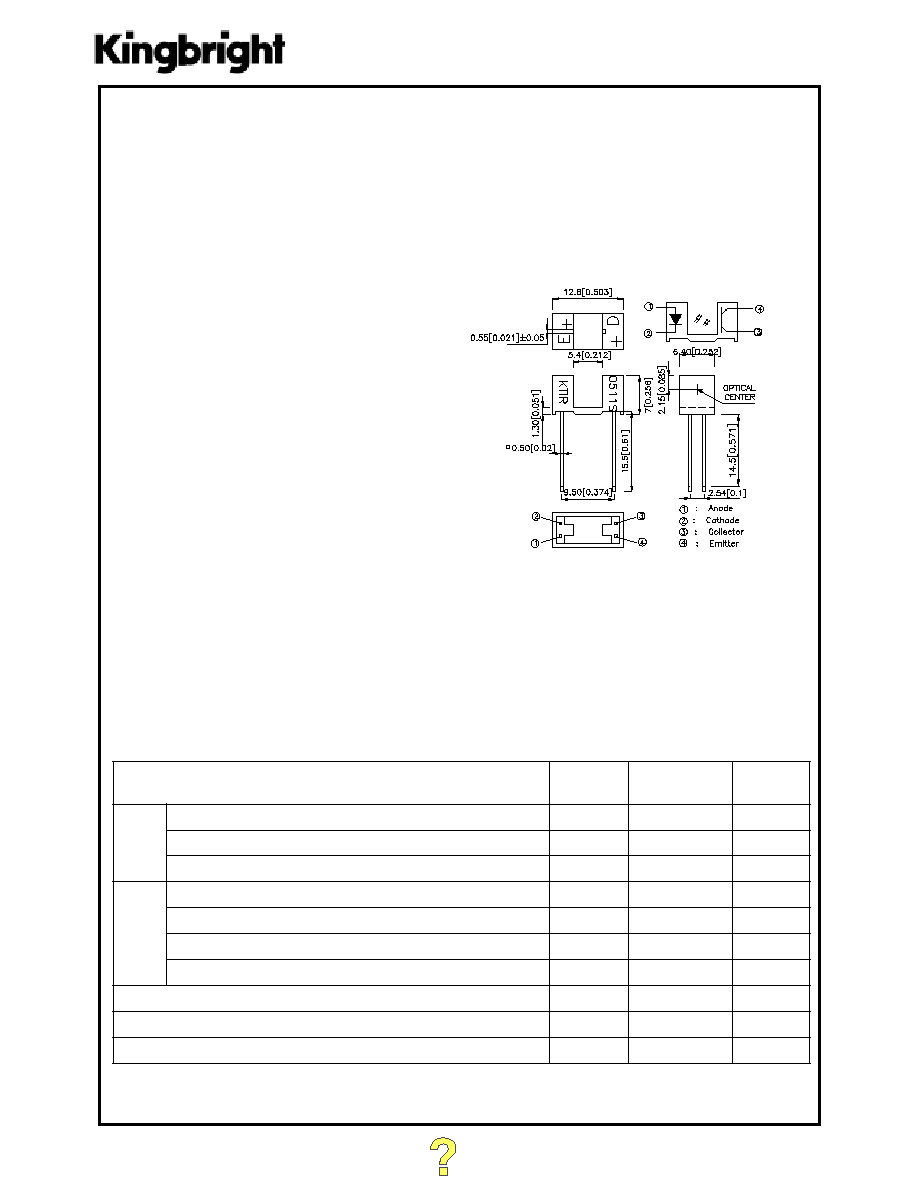
KTIR0511S
PHOTO-INTERRUPTER
Notes:
1. All dimensions are in millimeters (inches).
2. Tolerance is
±
0.15(0.006") unless otherwise noted.
3. Lead spacing is measured where the lead emerge package.
4. Specifications are subject to change without notice.
Features
!
Ultra-small
!
Minimal influence from stray light
!
Low collector-emitter saturation voltage
Applications
!
Optical control equipment.
!
Cameras.
!
Floppy disk drives.
Package Dimensions
Absolute Maximum Ratings (T
=
=25
∞∞
∞∞
∞
C)
r
e
t
e
m
a
r
a
P
r
e
t
e
m
a
r
a
P
r
e
t
e
m
a
r
a
P
r
e
t
e
m
a
r
a
P
r
e
t
e
m
a
r
a
P
l
o
b
m
y
S
l
o
b
m
y
S
l
o
b
m
y
S
l
o
b
m
y
S
l
o
b
m
y
S
g
n
it
a
R
g
n
it
a
R
g
n
it
a
R
g
n
it
a
R
g
n
it
a
R
ti
n
U ti
n
U ti
n
U ti
n
U ti
n
U
t
u
p
n
I
t
n
e
rr
u
c
d
r
a
w
r
o
F
I
F
0
5
A
m
e
g
a
tl
o
v
e
s
r
e
v
e
R
V
R
5
V
n
o
it
a
p
i
s
s
i
d
r
e
w
o
P
P
5
7
W
m
t
u
p
t
u
O
e
g
a
tl
o
v
r
e
tt
i
m
e
-r
o
t
c
e
ll
o
C
V
O
E
C
0
3
V
e
g
a
tl
o
v
r
o
t
c
e
ll
o
c
-r
e
tt
i
m
E
V
O
C
E
5
V
t
n
e
rr
u
c
r
o
t
c
e
ll
o
C
I
C
0
2
A
m
n
o
it
a
p
i
s
s
i
d
r
e
w
o
p
r
o
t
c
e
ll
o
C
P
C
5
7
W
m
e
r
u
t
a
r
e
p
m
e
t
g
n
it
a
r
e
p
O
r
p
o
T
5
8
+
~
5
2
-
∞
C
e
r
u
t
a
r
e
p
m
e
t
e
g
a
r
o
t
S
g
t
s
T
0
0
1
+
~
0
4
-
∞
C
)
s
d
n
o
c
e
s
5
r
o
f
y
d
o
b
m
o
rf
h
c
n
i
6
1
/
1
(
e
r
u
t
a
r
e
p
m
e
t
g
n
ir
e
d
l
o
S
l
o
s
T
0
6
2
∞
C
Digitally signed by wyne chiu
cn=wyne chiu, c=CN
Date: 2001.11.07 11:00:43 +08'00'
Reason: <none>
shenzheng

SPEC NO: KDA0659
REV NO: V.1
DATE: OCT/30/2001
PAGE: 2 OF3
APPROVED: J.Lu
CHECKED :
DRAWN: X.H.FU
Electro-optical Characteristics (T
a
=25
∞∞
∞∞
∞
C)
Fig.1 Forward Current vs.
Forward Voltage
Fig.2 Collector Current vs.
Forward Current
Fig.3 Collector Current vs.
Collector-emitter Voltage
r
e
t
e
m
a
r
a
P
r
e
t
e
m
a
r
a
P
r
e
t
e
m
a
r
a
P
r
e
t
e
m
a
r
a
P
r
e
t
e
m
a
r
a
P
l
o
b
m
y
S
l
o
b
m
y
S
l
o
b
m
y
S
l
o
b
m
y
S
l
o
b
m
y
S
s
n
o
it
i
d
n
o
C
s
n
o
it
i
d
n
o
C
s
n
o
it
i
d
n
o
C
s
n
o
it
i
d
n
o
C
s
n
o
it
i
d
n
o
C
.
n
i
M .
n
i
M .
n
i
M .
n
i
M .
n
i
M
.
p
y
T .
p
y
T .
p
y
T .
p
y
T .
p
y
T
.
x
a
M .
x
a
M .
x
a
M .
x
a
M .
x
a
M
ti
n
U ti
n
U ti
n
U ti
n
U ti
n
U
t
u
p
n
I
e
g
a
tl
o
v
d
r
a
w
r
o
F
V
F
I
F
A
m
0
2
=
_
2
.
1
5
.
1
V
t
n
e
r
r
u
c
e
s
r
e
v
e
R
I
R
V
R
V
5
=
_
_
0
1
µ
A
t
u
p
t
u
O
t
n
e
r
r
u
c
k
r
a
d
r
o
t
c
e
ll
o
C
I
O
E
C
V
E
C
V
0
2
=
_
_
0
0
1
A
n
r
e
f
s
n
a
r
T
-t
c
a
r
a
h
c
s
c
it
s
ir
e
e
g
a
tl
o
v
n
o
it
a
r
u
t
a
s
r
e
tt
i
m
e
-
r
o
t
c
e
ll
o
C
V
)t
a
s
(
E
C
I
C
A
m
1
=
I
F
A
m
0
4
=
_
_
4
.
0
V
o
it
a
r
r
e
f
s
n
a
rt
t
n
e
r
r
u
C
R
T
C
V
E
C
V
5
=
I
F
A
m
0
2
=
_
0
1
_
%
e
m
it
e
s
n
o
p
s
e
R
e
m
it
e
s
i
R
t
r
V
E
C
V
2
=
I
C
A
m
2
=
R
L
0
0
1
=
_
5
5
2
µ
c
e
s
e
m
it
ll
a
F
t
f
_
4
0
2
µ
c
e
s
Digitally signed by wyne chiu
cn=wyne chiu, c=CN
Date: 2001.11.07 11:01:02 +08'00'
Reason: <none>
shenzheng
SPEC NO: CDA0659
REV NO: V.1
DATE: OCT/30/2001
PAGE: 3 OF3
APPROVED: J.Lu
CHECKED :
DRAWN: X.H.FU
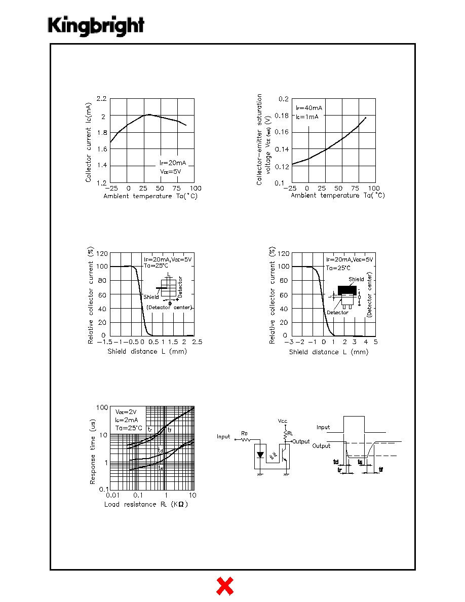
Fig.4 Collector Current vs.
Ambient Temperature
Fig.5 Collector-emitter Saturation
Voltage vs. Ambient Temperature
Fig.6 Relative Collector Current vs.
Shield Distance(1)
Fig.7 Relative Collector Current vs.
Shield Distance(2)
Fig.8 Response Time vs.
Load Resistance
Test Circuit for Response Time
Digitally signed by wyne chiu
cn=wyne chiu, c=CN
Date: 2001.11.07 11:01:17 +08'00'
Reason: <none>
shenzheng