
Eastman Kodak Company ≠ Image Sensor Solutions - Rochester, NY 14650-2010
Phone (716) 722-4385 Fax (716) 477-4947
Web: www.kodak.com/go/ccd E-mail: ccd@kodak.com
1
Revision No. 1
KAF-1602LE
Performance Specification
KAF- 1602LE
1536 (H) x 1024 (V) Pixel
Enhanced Response
Full-Frame CCD Image Sensor
With Anti-Blooming Protection
Performance Specification
Eastman Kodak Company
Image Sensor Solutions
Rochester, New York 14650-2010
Revision 1
March 19, 2001

Eastman Kodak Company ≠ Image Sensor Solutions - Rochester, NY 14650-2010
Phone (716) 722-4385 Fax (716) 477-4947
Web: www.kodak.com/go/ccd E-mail: ccd@kodak.com
2
Revision No.1
KAF-1602LE
Performance Specification
TABLE OF CONTENTS
1.1 Features...............................................................................................................................................3
1.2 Description..........................................................................................................................................3
1.3 Image Acquisition...............................................................................................................................4
1.4 Charge Transport ................................................................................................................................4
1.5
Output Structure..................................................................................................................................4
1.6
Dark Reference Pixels ........................................................................................................................4
1.7
Dummy Pixels ....................................................................................................................................4
2.1 Package Drawing ................................................................................................................................5
2.2 Pin Description ...................................................................................................................................6
3.1 Absolute Maximum Ratings ...............................................................................................................7
3.2 DC Operating Conditions ...................................................................................................................8
3.3 AC Operating Conditions ...................................................................................................................9
3.4 AC Timing Conditions .......................................................................................................................9
4.1 Performance Specifications ..............................................................................................................11
4.2 Typical Performance Characteristics ................................................................................................12
4.3 Defect Classification.........................................................................................................................13
5.1 Quality Assurance and Reliability ....................................................................................................14
5.2 Ordering Information........................................................................................................................14
Revision Changes ...................................................................................................................................15
FIGURES
Figure 1
Functional Block Diagram 3
Figure 2
Packaging Diagram 5
Figure 3
Packaging Pin Designations 6
Figure 4
Recommended Output Structure Load Diagram 8
Figure 5
Timing Diagrams 10

Eastman Kodak Company ≠ Image Sensor Solutions - Rochester, NY 14650-2010
Phone (716) 722-4385 Fax (716) 477-4947
Web: www.kodak.com/go/ccd E-mail: ccd@kodak.com
3
Revision No.1
KAF-1602LE
Performance Specification
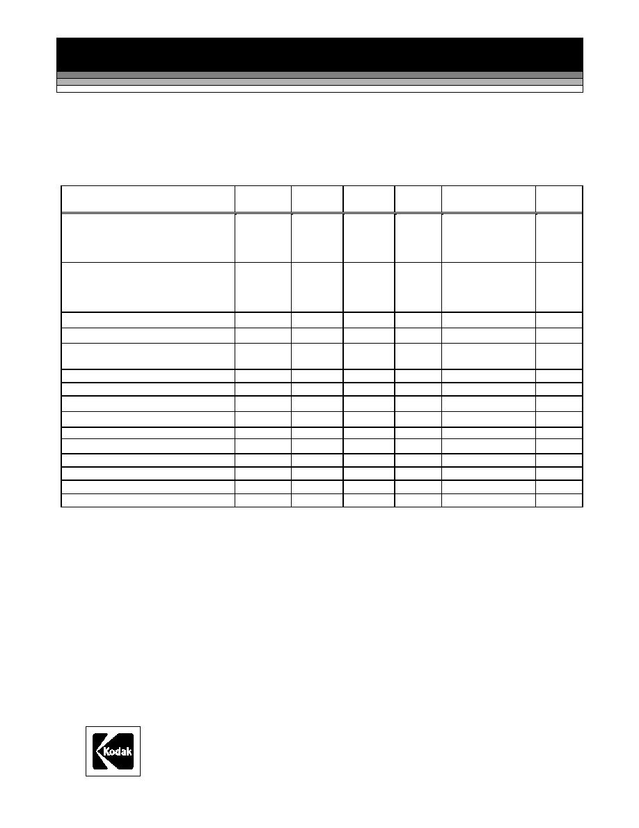
1.1
Features
1.6M Pixel Area CCD
1536H x 1024V (9
µ
µ
µ
µ
m) Pixels
13.8 mm H x 9.2 mm V Photosensitive Area
2-Phase Register Clocking
Enhanced Responsivity
70% Fill Factor
Antiblooming Protection
Low Dark Current ( <10pA/cm2 @ 25oC)
1.2
Description
The KAF-1602 is a high performance monochrome area
CCD (charge-coupled device) image sensor with 1536H
x 1024V photoactive pixels designed for a wide range
of image sensing applications in the 0.4nm to 1.0nm
wavelength band. Typical applications include military,
scientific, and industrial imaging. A 74dB dynamic
range is possible operating at room temperature.
The sensor is built with a true two-phase CCD
technology employing a transparent gate.
This technology simplifies the support circuits that
drive the sensor and reduces the dark current without
compromising charge capacity. The transparent gate
results in spectral response increased ten times at
400nm, compared to a front side illuminated standard
poly silicon gate technology. The sensitivity is
increased 50% over the rest of the visible wavelengths.
Total chip size is 13.8mm x 9.2mm and is housed in a
24-pin, 0.88" wide DIL ceramic package with 0.1" pin
spacing.
The sensor consists of 1552 parallel (vertical) CCD
shift registers each 1032 elements long. These registers
act as both the photosensitive elements and as the
transport circuits that allow the image to be sequentially
read out of the sensor. The elements of these registers
are arranged into a 1536 x 1024 photosensitive array
surrounded by a light shielded dark reference of 16
columns and 8 rows. The parallel (vertical) CCD
registers transfer the image one line at a time into a
single 1564 element (horizontal) CCD shift register.
The horizontal register transfers the charge to a single
output amplifier. The output amplifier is a two-stage
source follower that converts the photo-generated
charge to a voltage for each pixel.
KAF ≠ 1602LE
Usable Active Image Area
1536(H) x 1024(V)
9 x 9
µ
m pixels
3:2 aspect ratio
1536 Active Pixels/Line
4 Dark
10 Inactive
Vrd
R
Vdd
Vout
Vss
Sub
Vog
H1
H2
V1
V2
Guard
2 Inactive
12 Dark
4 Dark lines
4 Dark lines
Figure 1 - Functional Block Diagram

Eastman Kodak Company ≠ Image Sensor Solutions - Rochester, NY 14650-2010
Phone (716) 722-4385 Fax (716) 477-4947
Web: www.kodak.com/go/ccd E-mail: ccd@kodak.com
4
Revision No.1
KAF-1602LE
Performance Specification
1.3
Image Acquisition
An electronic representation of an image is formed
when incident photons falling on the sensor plane create
electron-hole pairs within the sensor. These photon
induced electrons are collected locally by the formation
of potential wells at each photogate or pixel site. The
number of electrons collected is linearly dependent on
light level and exposure time and non-linearly
dependent on wavelength. When the pixel's capacity is
reached, excess electrons will spill into the lateral
overflow drain (LOD) and drain off chip, thus isolating
adjacent pixels from the excess signal. This is termed
anti-blooming protection. During the integration period,
the
V1 and
V2 register clocks are held at a constant
(low) level.
See Figure 5. - Timing Diagrams.
The antiblooming capability is provided by a lateral
overflow drain structure. This type of antiblooming
design consumes thirty percent of the pixel area and
reduces the saturation signal and quantum efficiency
proportionately. However, it maintains the broad
spectral response from 400 to 1000nm and good linear
response up to saturation.
1.4
Charge Transport
Referring again to Figure 5 - Timing Diagrams, the
integrated charge from each photogate is transported to
the output using a two step process. Each line (row) of
charge is first transported from the vertical CCDs to the
horizontal CCD register using the
V1 and
V2 register
clocks. The horizontal CCD is presented a new line on
the falling edge of
V2 while
H1 is held high. The
horizontal CCDs then transport each line, pixel by
pixel, to the output structure by alternately clocking the
H1 and
H2 pins in a complementary fashion. On each
falling edge of
H2 a new charge packet is transferred
onto a floating diffusion and sensed by the output
amplifier
1.5
Output Structure
Charge presented to the floating diffusion (FD) is
converted into a voltage and current amplified in order
to drive off-chip loads. The resulting voltage change
seen at the output is linearly related to the amount of
charge placed on FD.
Once the signal has been sampled by the system
electronics, the reset gate (
R) is clocked to remove the
signal and FD is reset to the potential applied by VRD.
More signal at the floating diffusion reduces the voltage
seen at the output pin. In order to activate the output
structure, an off-chip load must be added to the Vout
pin of the device - see Figure 4
1.6
Dark Reference Pixels
Surrounding the peripheral of the device is a border of
light shielded pixels. This includes 4 leading and 12
trailing pixels on every line excluding dummy pixels.
There are also 4 full dark lines at the start of every
frame and 4 full dark lines at the end of each frame.
Under normal circumstances, these pixels do not
respond to light. However, dark reference pixels in
close proximity to an active pixel, or the outer bounds
of the chip (including the first two lines out), can
scavenge signal depending on light intensity and
wavelength and therefore will not represent the true
dark signal.
1.7
Dummy Pixels
Within the horizontal shift register are 10 leading and 2
trailing additional shift phases that are not associated
with a column of pixels within the vertical register.
These pixels contain only horizontal shift register dark
current and do not respond to light. A few leading
dummy pixels may scavenge false signal depending on
operating conditions.
Eastman Kodak Company ≠ Image Sensor Solutions - Rochester, NY 14650-2010
Phone (716) 722-4385 Fax (716) 477-4947
Web: www.kodak.com/go/ccd E-mail: ccd@kodak.com
5
Revision No. 1
KAF-1602LE
Performance Specification
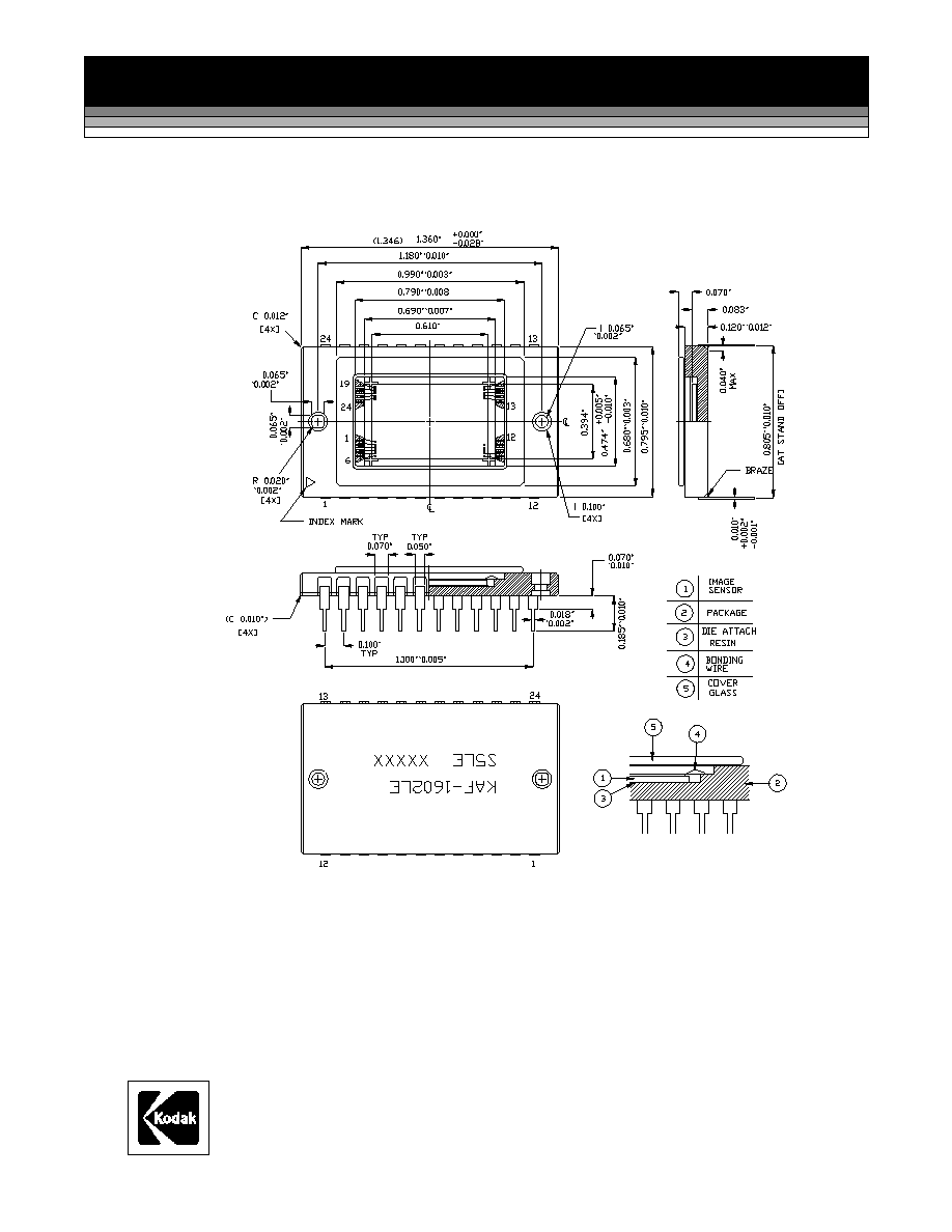
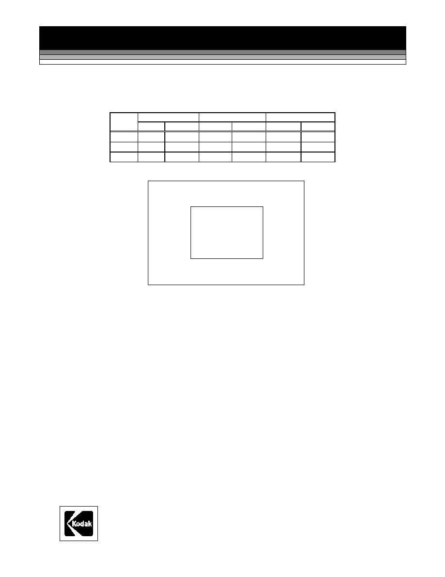
2.1
Package Drawing
Figure 2 ≠ Package Drawing
Eastman Kodak Company ≠ Image Sensor Solutions - Rochester, NY 14650-2010
Phone (716) 722-4385 Fax (716) 477-4947
Web: www.kodak.com/go/ccd E-mail: ccd@kodak.com
6
Revision No.1
KAF-1602LE
Performance Specification
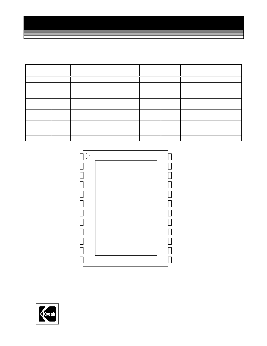
2.2
Pin Description
Pin
Symbol
Description
Pin
Symbol
Description
1
VOG
Output Gate
13
N/C
No connection (open pin)
2
VOUT
Video Output
11, 14
VSUB
Substrate (Ground)
3
VDD
Amplifier Supply
15, 16,
21, 22
V1
Vertical CCD Clock - Phase 1
4
VRD
Reset Drain
17, 18,
19, 20
V2
Vertical CCD Clock - Phase 2
5
R
Reset Clock
23
Guard
Guard Ring
6
VSS
Amplifier Supply Return
24
N/C
No Connection (open pin)
7
H1
Horizontal CCD Clock - Phase 1
8
H2
Horizontal CCD Clock - Phase 2
9, 10, 12
N/C
No connection (open pin)
Figure 3 - Packaging Pin Designations
Pin 1
Pixel 1,1
1
2
3
4
5
6
7
8
9
10
11
12
VOG
Vout
VDD
VRD
R
24
23
22
21
20
19
18
17
16
15
14
13
Guard
V1
V1
Vsub
V2
V2
V2
V2
V1
H2
H1
VSS
V1
N/C
N/C
N/C
N/C
Vsub
N/C
Eastman Kodak Company ≠ Image Sensor Solutions - Rochester, NY 14650-2010
Phone (716) 722-4385 Fax (716) 477-4947
Web: www.kodak.com/go/ccd E-mail: ccd@kodak.com
7
Revision No.1
KAF-1602LE
Performance Specification
3.1
Absolute Maximum Ratings
Description
Symbol
Min.
Max.
Units
Notes
Diode Pin Voltages
Vdiode
0
20
V
1, 2
Gate Pin Voltages - Type 1
Vgate1
-16
16
V
1, 3
Gate Pin Voltages - Type 2
Vgate2
0
16
V
1, 4
Inter-Gate Voltages
Vg-g
16
V
5
Output Bias Current
Iout
-10
mA
6
Output Load Capacitance
Cload
15
pF
6
Storage Temperature
T
100
o
C
Humidity
RH
5
90
%
7
Notes:
1.
Referenced to pin VSUB.
2.
Includes pins: VRD, VDD, VSS, VOUT.
3.
Includes pins:
V1,
V2,
H1,
H2.
4.
Includes pins:
R, VOG.
5.
Voltage difference between overlapping gates. Includes:
V1 to
V2,
H1 to
H2,
V2 to
H1,
H2 to VOG.
6.
Avoid shorting output pins to ground or any low impedance source during operation.
7.
T=25
∞
C. Excessive humidity will degrade MTTF.
CAUTION:
This device contains limited protection against Electrostatic Discharge (ESD). Devices should be handled
in accordance with strict ESD control procedures for Class 1 devices.

Eastman Kodak Company ≠ Image Sensor Solutions - Rochester, NY 14650-2010
Phone (716) 722-4385 Fax (716) 477-4947
Web: www.kodak.com/go/ccd E-mail: ccd@kodak.com
8
Revision No.1
KAF-1602LE
Performance Specification
3.2
DC Operating Conditions
Description
Symbol
Min.
Nom.
Max.
Units
Max DC Current
(mA)
Notes
Reset Drain
VRD
10.5
11
11.5
V
0.01
Output Amplifier Return
VSS
1.5
2.0
2.5
V
-0.5
Output Amplifier Supply
VDD
14.5
15
15.5
V
Iout
Substrate
VSUB
0
0
0
V
0.01
Output Gate
VOG
3.75
4
5
V
0.01
Guard Ring
Guard
8.0
9.0
12.0
V
0.01
Video Output Current
Iout
-5
-10
mA
-
1
Notes:
1.
An output load sink must be applied to Vout to activate output amplifier - see Figure below.
+15V
0.1uF
Vout
Buffered Output
1k
140
2N3904 or equivalent
~5ma
Figure 4 - Recommended Output Structure Load Diagram
Eastman Kodak Company ≠ Image Sensor Solutions - Rochester, NY 14650-2010
Phone (716) 722-4385 Fax (716) 477-4947
Web: www.kodak.com/go/ccd E-mail: ccd@kodak.com
9
Revision No.1
KAF-1602LE
Performance Specification
3.3
AC Operating Condition
Description
Symbol
Level
Min.
Nom.
Max.
Units
Effective
Capacitance
Notes
Vertical CCD Clock - Phase 1
V1
Low
High
-10.5
0
-10.0
0.5
-9.5
1.0
V
V
21 nF
(all ¢V1
pins)
Vertical CCD Clock - Phase 2
V2
Low
High
-10.5
0
-10.0
0.5
-9.5
1.0
V
V
21 nF
(all ¢V2
pins)
Horizontal CCD Clock - Phase 1
H1
Low
High
-5.0
5.0
-4.0
6.0
-3.5
6.5
V
V
200pF
Horizontal CCD Clock - Phase 2
H2
Low
High
-5.0
5.0
-4.0
6.0
-3.5
6.5
V
V
200pF
Reset Clock
R
Low
High
-4
3.5
-3
4.0
-2
5.0
V
V
5pF
Notes:
1.
All pins draw less than 10uA DC current.
2.
Capacitance values relative to VSUB.
3.4
AC Timing Conditions
Description
Symbol
Min.
Nom.
Max.
Units
Notes
H1,
H2 Clock Frequency
f
H
10
15
MHz
1, 2, 3
V1,
V2 Clock Frequency
f
V
100
125
kHz
1, 2, 3
Pixel Period (1 Count)
t
e
67
100
ns
H1,
H2 Setup Time
t
HS
0.5
1
us
V1,
V2 Clock Pulse Width
t
V
4
5
us
2
Reset Clock Pulse Width
t
R
10
20
ns
4
Readout Time
t
readout
121
178
ms
5
Integration Time
t
int
6
Line Time
tline
117.4
172.5
us
7
Notes:
1.
50% duty cycle values.
2.
CTE may degrade above the nominal frequency.
3.
Rise and fall times (10/90% levels) should be limited to 5-10% of clock period. Cross-over of register clocks should be between
40-60% of amplitude.
4.
R should be clocked continuously.
5.
t
readout
= ( 1032 * tline )
6.
Integration time is user specified. Longer integration times will degrade noise performance.
7.
tline = ( 3* t
V
) + t
HS
+ ( 1564 * t
e
) + t
e

Eastman Kodak Company ≠ Image Sensor Solutions - Rochester, NY 14650-2010
Phone (716) 722-4385 Fax (716) 477-4947
Web: www.kodak.com/go/ccd E-mail: ccd@kodak.com
10
Revision No.1
KAF-1602LE
Performance Specification
Frame Timing
tReadout
Line
1
2
1031
1032
1 Frame = 1032 Lines
V1
V2
H1
H2
tint
Pixel Timing Detail
R
H1
H2
Vout
t
R
Vsat
Vdark
Vsub
Vodc
1 count
te
Line Timing Detail
1 line
V1
V2
H1
H2
R
1564 counts
t
HS
te
t
V
t
V
Vpix
Line Content
Photoactive Pixels
Dark Reference Pixels
Dummy Pixels
1-10 11-14
15 - 1550
1551-1562 1563-1564
Vsat Saturated pixel video output signal
Vdark Video output signal in no light situation, not zero due to Jdark
Vpix Pixel video output signal level, more electrons =more negative*
Vodc Video level offset with respect to vsub
Vsub Analog Ground
* See Image Aquisition section (page 4)
Figure 5 - Timing Diagrams
Eastman Kodak Company ≠ Image Sensor Solutions - Rochester, NY 14650-2010
Phone (716) 722-4385 Fax (716) 477-4947
Web: www.kodak.com/go/ccd E-mail: ccd@kodak.com
11
Revision No.1
KAF-1602LE
Performance Specification
4.1
Performance Specifications
All values measured at 25
∞
C, and nominal operating conditions. These parameters exclude defective pixels.
Description
Symbol
Min.
Nom.
Max.
Units
Notes
Saturation Signal
Vertical CCD capacity
Horizontal CCD capacity
Output Node capacity
Nsat
45000
170000
190000
50000
200000
220000
65000
240000
240000
electrons / pixel
1
Red Quantum Efficiency (
=650nm)
Green Quantum Efficiency (
=550nm)
Blue Quantum Efficiency (
=450nm)
Blue Quantum Efficiency (
=400nm)
Rr
Rg
Rb
Rb 400
42
35
20
16
%
%
%
%
Photoresponse Non-Linearity
PRNL
1
2
%
2
Photoresponse Non-Uniformity
PRNU
1
3
%
3
Dark Signal
Jdark
15
2.1
35
7
electrons / pixel / sec
pA/cm2
4
Dark Signal Doubling Temperature
5
6.3
7.5
o
C
Dark Signal Non-Uniformity
DSNU
15
50
electrons / pixel / sec
5
Dynamic Range
DR
67
70
dB
6
Charge Transfer Efficiency
CTE
0.99997
0.99999
Output Amplifier DC Offset
Vodc
9.5
10.5
11.5
V
7
Output Amplifier Bandwidth
f-3dB
45
Mhz
8
Output Amplifier Sensitivity
Vout/Ne~
9
10
11
uV/e~
Output Amplifier output Impedance
Zout
175
200
250
Ohms
Noise Floor
ne~
15
20
electrons
9
Antiblooming Protection
Vab
128
Saturation exposure
10
Notes:
1.
For pixel binning applications, electron capacity up to 330000 can be achieved with modified CCD inputs.
Each sensor may have to be optimized individually for these applications. Some performance parameters may be compromised to
achieve the largest signals.
2.
Worst case deviation from straight line fit, between 1% and 90% of Vsat.
3.
One Sigma deviation of a 128x128 sample when CCD illuminated uniformly.
4.
Average of all pixels with no illumination at 25
o
C..
5.
Average dark signal of any of 12 x 8 blocks within the sensor. (each block is 128 x 128 pixels)
6.
20log ( Nsat / ne~) at nominal operating frequency and 25
o
C.
7.
Video level offset with respect to ground
8.
Last output amplifier stage only. Assumes 10pF off-chip load..
9.
Output noise at 25
o
C , nominal operating frequency, and tint = 0.
10.
Number of times above the Vsat illumination level required to cause 50% distortion in a test pattern consisting of a bright circular
region approximately 1/10 the size of the image sensor. In most systems a 128x optical overload will cause flare from reflections
that mask the performance of the image sensor.

Eastman Kodak Company ≠ Image Sensor Solutions - Rochester, NY 14650-2010
Phone (716) 722-4385 Fax (716) 477-4947
Web: www.kodak.com/go/ccd E-mail: ccd@kodak.com
12
Revision No.1
KAF-1602LE
Performance Specification
4.2
Typical Performance Characteristics
Spectral Response
KAF-1602LE
0
0.05
0.1
0.15
0.2
0.25
0.3
0.35
0.4
0.45
0.5
400
500
600
700
800
900
1000
1100
Wavelength (nm)
Absolute Quantum Efficiency
(electrons/photon)
Eastman Kodak Company ≠ Image Sensor Solutions - Rochester, NY 14650-2010
Phone (716) 722-4385 Fax (716) 477-4947
Web: www.kodak.com/go/ccd E-mail: ccd@kodak.com
13
Revision No.1
KAF-1602LE
Performance Specification
4.3
Cosmetic Classification
All tests performed at T=25
o
C
Class
Point Defects
Cluster Defects
Column Defects
Total
Zone A
Total
Zone A
Total
Zone A
C1
5
2
0
0
0
0
C2
10
5
4
2
0
0
C3
20
10
8
4
4
2
1536,1024
1,1
1536,1
1,1024
368,212
1168,212
1168,812
368,812
Zone A
Center 800 x 600 Pixels
Point Defect
DARK: A pixel which deviates by more than 6% from
neighboring pixels when illuminated to 70% of saturation, OR
BRIGHT: A Pixel with dark current > 3000 e/pixel/sec at
25C.
Cluster Defect
A grouping of not more than 5 adjacent point defects
Column Defect
A grouping of >5 contiguous point defects along a single
column, OR
A column containing a pixel with dark current >
6,000e/pixel/sec, OR A column that does not meet the
minimum vertical CCD charge capacity, OR
A column which loses more than 250 e under 2Ke
illumination.
Neighboring pixels
The surrounding 128 x 128 pixels or
±
64 columns/rows.
Defect Separation
Column and cluster defects are separated by no less than two
(2) pixels in any direction (excluding single pixel defects).
Defect Region Exclusion Defect region excludes the outer two (2) rows and columns at each side/end of
the sensor.

Eastman Kodak Company ≠ Image Sensor Solutions - Rochester, NY 14650-2010
Phone (716) 722-4385 Fax (716) 477-4947
Web: www.kodak.com/go/ccd E-mail: ccd@kodak.com
14
Revision No.1
KAF-1602LE
Performance Specification
5.1
Quality Assurance and Reliability
5.1.1
Quality Strategy: All devices will conform to the specifications stated in this document. This is accomplished
through a combination of statistical process control and inspection at key points of the production process.
5.1.2
Replacement: All devices are warranted against failure in accordance with the terms of Terms of Sale.
5.1.3
Cleanliness: Devices are shipped free of contamination, scratches, etc. that would cause a visible defect.
5.1.4
ESD Precautions: Devices are shipped in a static-safe container and should only be handled at static-safe work
stations.
5.1.5
Reliability: Information concerning the quality assurance and reliability testing procedures and results are available
from the Image Sensor Solutions and can be supplied upon request.
5.1.6
Test Data Retention: Devices have an identifying number of traceable to a test data file. Test data is kept for a
period of 2 years after date of shipment.
5.2
Ordering Information
See Appendix 1 for available part numbers
Address all inquiries and purchase orders to:
Image Sensor Solutions
Eastman Kodak Company
Rochester, New York 14650-2010
Phone: (716) 722-4385
Fax:
(716) 477-4947
E-mail:
ccd@kodak.com
Web:
www.kodak.com/go/ccd
Kodak reserves the right to change any information contained herein without notice. All information furnished by
Kodak is believed to be accurate.
WARNING: LIFE SUPPORT APPLICATIONS POLICY
Kodak image sensors are not authorized for and should not be used within Life Support Systems without the
specific written consent of the Eastman Kodak Company. Product warranty is limited to replacement of
defective components and does not cover injury or property or other consequential damages.

Eastman Kodak Company ≠ Image Sensor Solutions - Rochester, NY 14650-2010
Phone (716) 722-4385 Fax (716) 477-4947
Web: www.kodak.com/go/ccd E-mail: ccd@kodak.com
15
Revision No.1
KAF-1602LE
Performance Specification
Revision Changes
Revision
Number
Description of Changes
0
Original formal version.
1
Eliminated Class 0.
Eliminated Appendix 1 ≠ Available Part Numbers.
Added Revision Changes.