
K A I - 0 3 3 0 S R e v 2 . 0
w w w . k o d a k . c o m / g o / i m a g e r s 5 8 5 - 7 2 2 - 4 3 8 5 i m a g e r s @ k o d a k . c o m
IMAGE SENSOR SOLUTIONS
D E V I C E
P E R F O R M A N C E
S P E C I F I C A T I O N
KODAK KAI-0330S
Image Sensor
648 (H) x 484 (V)
Interline Transfer
Progressive Scan CCD
June 2, 2003
Revision 2.0

K A I - 0 3 3 0 S R e v 2 . 0
w w w . k o d a k . c o m / g o / i m a g e r s 5 8 5 - 7 2 2 - 4 3 8 5 i m a g e r s @ k o d a k
IMAGE SENSOR SOLUTIONS
2
Table of Contents
Features ......................................................................................................................................................... 5
Description .................................................................................................................................................... 6
Architecture................................................................................................................................................... 6
Image Acquisition ......................................................................................................................................... 6
Charge Transport........................................................................................................................................... 6
Output Structure ............................................................................................................................................ 7
Electronic Shutter.......................................................................................................................................... 8
Color Filter Array (optional, for KAI-0330SCM only) ................................................................................ 8
Packaging Configuration............................................................................................................................... 9
Marking Code................................................................................................................................................ 9
Pin Description............................................................................................................................................ 10
Absolute Maximum Range.......................................................................................................................... 11
DC Operating Conditions............................................................................................................................ 12
AC Clock Level Conditions ........................................................................................................................ 13
AC Timing Requirements for 30 MHz Operation....................................................................................... 14
Frame Timing .................................................................................................................................... 15
Line Timing....................................................................................................................................... 16
Pixel Timing...................................................................................................................................... 17
Electronic Shutter Timing ................................................................................................................. 18
Fast Dump Timing ≠ Removing Four Lines ..................................................................................... 19
Binning ≠ Two to One Line Binning................................................................................................. 20
Timing ≠ Sample Video Waveform .................................................................................................. 21
Image Specifications ................................................................................................................................... 22
Electro-Optical for KAI-0330SCM................................................................................................... 22
Electro-Optical for KAI-0330SM ..................................................................................................... 24
CCD................................................................................................................................................... 26
Output Amplifier @ V
DD
= 15V, V
SS
= 0.0V.................................................................................... 26
General .............................................................................................................................................. 27
Defect Classification ................................................................................................................................... 30
Climatic Requirements ................................................................................................................................ 31
Quality Assurance and Reliability............................................................................................................... 31
Ordering Information .................................................................................................................................. 32
Revision Changes........................................................................................................................................ 33

K A I - 0 3 3 0 S R e v 2 . 0
w w w . k o d a k . c o m / g o / i m a g e r s 5 8 5 - 7 2 2 - 4 3 8 5 i m a g e r s @ k o d a k
IMAGE SENSOR SOLUTIONS
3
Figures
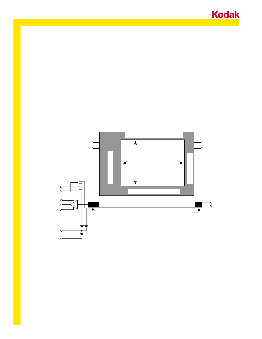
Figure 1 Functional Block Diagram.............................................................................................................. 5
Figure 2 Output Structure.............................................................................................................................. 7
Figure 3 CFA Pattern .................................................................................................................................... 8
Figure 4 Device Drawing ≠ Die Placement................................................................................................... 9
Figure 5 Pinout Diagram Top View............................................................................................................ 10
Figure 6 Recommended Output Structure Load Diagram........................................................................... 12
Figure 7 Frame Timing................................................................................................................................ 15
Figure 8 Line Timing .................................................................................................................................. 16
Figure 9 Pixel Timing Diagram................................................................................................................... 17
Figure 10 Electronic Shutter Timing Diagram............................................................................................ 18
Figure 11 Fast Line Dump Timing - Removing Four Lines ....................................................................... 19
Figure 12 Binning - 2 to 1 Line Binning..................................................................................................... 20
Figure 13 Sample Video Waveform at 5MHz............................................................................................. 21
Figure 14 Nominal KAI 0330SCM Spectral Response .............................................................................. 23
Figure 15 Nominal KAI-0330SM Spectral Response................................................................................. 24
Figure 16 Angular Dependence on Quantum Efficiency ............................................................................ 25
Figure 17 Typical KAI-0330S Series Photoresponse ................................................................................. 27
Figure 18 Example of Vsat versus Vsub..................................................................................................... 28
Figure 19 Frame Rate versus Horizontal Clock Frequency ........................................................................ 29

K A I - 0 3 3 0 S R e v 2 . 0
w w w . k o d a k . c o m / g o / i m a g e r s 5 8 5 - 7 2 2 - 4 3 8 5 i m a g e r s @ k o d a k
IMAGE SENSOR SOLUTIONS
4
Tables
Table 1 Package Pin Assignments .............................................................................................................. 10
Table 2 Absolute Maximum Ranges ........................................................................................................... 11
Table 3 DC Operating Conditions............................................................................................................... 12
Table 4 AC Clock Level Conditions ........................................................................................................... 13
Table 5 AC Timing Requirements for 30 MHz Operation ......................................................................... 14
Table 6 Electro-Optical Image Specifications KAI-0330SCM................................................................... 22
Table 7 Electro-Optical Image Specifications KAI-0330SM ..................................................................... 24
Table 8 CCD Image Specifications ............................................................................................................. 26
Table 9 Output Amplifier Image Specifications ......................................................................................... 26
Table 10 General Image Specifications ...................................................................................................... 27
Table 11 Climatic Requirements................................................................................................................. 31
K A I - 0 3 3 0 S R e v 2 . 0
w w w . k o d a k . c o m / g o / i m a g e r s 5 8 5 - 7 2 2 - 4 3 8 5 i m a g e r s @ k o d a k
IMAGE SENSOR SOLUTIONS
5
Features
∑
Front Illuminated Interline Architecture
∑
648 (H) x 484 (V) Photosensitive Pixels
∑
9.0
µ
m(H) x 9.0
µ
m(V) Pixel Size
∑
5.83 mm(H) x 4.36 mm(V) Photosensitive Area
∑
Progressive Scan (Noninterlaced)
∑
Electronic Shutter
∑
Integral RGB Color Filter Array (optional)
∑
Advanced 2 Phase Buried Channel CCD
Processing
∑
On-Chip Dark Reference Pixels
∑
Low Dark Current
∑
Patented High Sensitivity Output Structure
∑
Antiblooming Protection
∑
Negligible Lag
∑
Low Smear (0.01% with microlens)
4 dark lines at bottom of image
8 dark lines at top of image
24
dar
k
col
u
mns
8 d
a
rk
co
lu
mn
s
KAI-0330
Active Image Area:
648 (H) x 484 (V)
9.0 x9.0
µ
m
2
pixels
Horizontal Register A
10 dummies
4 dummies
V1
V2
V1
V2
VOUTA
H1A
H2
VDD
VSS/OG
VRD
R
WELL
VSUB
4 dark lines at bottom of image
8 dark lines at top of image
24
dar
k
col
u
mns
8 d
a
rk
co
lu
mn
s
KAI-0330S
Active Image Area:
648 (H) x 484 (V)
9.0 x9.0
µ
m
2
pixels
Horizontal Register A
10 dummies
4 dummies
V1
V2
V1
V2
VOUTA
H1A
H2
VDD
VSS/OG
VRD
R
WELL
VSUB
Figure 1 Functional Block Diagram