
K A I - 1 1 0 0 0 R e v 3 . 0
w w w . k o d a k . c o m / g o / i m a g e r s 5 8 5 - 7 2 2 - 4 3 8 5 E m a i l : i m a g e r s @ k o d a k . c o m
IMAGE SENSOR SOLUTIONS
D E V I C E
P E R F O R M A N C E
S P E C I F I C A T I O N
KODAK KAI-11000M
KODAK KAI-11000CM
Image Sensor
4008 (H) x 2672 (V)
Interline Transfer
Progressive Scan CCD
June 2, 2003
Revision 3.0

K A I - 1 1 0 0 0 R e v 3 . 0
w w w . k o d a k . c o m / g o / i m a g e r s 5 8 5 - 7 2 2 - 4 3 8 5 E m a i l : i m a g e r s @ k o d a k . c o m
IMAGE SENSOR SOLUTIONS
2
TABLE OF CONTENTS
TABLE OF FIGURES................................................................................................................................................ 4
DEVICE DESCRIPTION .......................................................................................................................................... 5
DEVICE DESCRIPTION .......................................................................................................................................... 6
A
RCHITECTURE
......................................................................................................................................................... 6
O
VERALL
.................................................................................................................................................................. 6
Pixel..................................................................................................................................................................... 7
Vertical to Horizontal Transfer ........................................................................................................................... 8
Horizontal Register to Floating Diffusion........................................................................................................... 9
Horizontal Register Split ................................................................................................................................... 10
Single Output Operation ................................................................................................................................... 10
Dual Output Operation ..................................................................................................................................... 10
Output................................................................................................................................................................ 11
P
HYSICAL
D
ESCRIPTION
......................................................................................................................................... 12
Pin Description and Device Orientation ........................................................................................................... 12
PERFORMANCE..................................................................................................................................................... 13
P
OWER
- E
STIMATED
.............................................................................................................................................. 13
F
RAME
R
ATES
≠ C
ONTINUOUS
M
ODE
..................................................................................................................... 13
I
MAGING
P
ERFORMANCE
........................................................................................................................................ 14
Image Performance Operational Conditions .................................................................................................... 14
Imaging Performance Specifications................................................................................................................. 14
Defect Definitions.............................................................................................................................................. 16
Defect Map ........................................................................................................................................................ 16
Quantum Efficiency ........................................................................................................................................... 17
Angular Quantum Efficiency ............................................................................................................................. 18
TEST DEFINITIONS............................................................................................................................................... 19
T
EST
R
EGIONS OF
I
NTEREST
................................................................................................................................... 19
O
VER
C
LOCKING
..................................................................................................................................................... 19
Tests................................................................................................................................................................... 20
OPERATION ............................................................................................................................................................ 21
M
AXIMUM
R
ATINGS
............................................................................................................................................... 21
DC B
IAS
O
PERATING
C
ONDITIONS
......................................................................................................................... 21
AC O
PERATING
C
ONDITIONS
.................................................................................................................................. 22
Clock Levels ...................................................................................................................................................... 22
Clock Line Capacitances................................................................................................................................... 22
T
IMING
R
EQUIREMENTS
.......................................................................................................................................... 23
M
AIN
T
IMING
≠ C
ONTINUOUS
M
ODE
...................................................................................................................... 24
F
RAME
T
IMING
≠ C
ONTINUOUS
M
ODE
.................................................................................................................... 25
Frame Timing without Binning ......................................................................................................................... 25
Frame Timing for Vertical Binning by 2 ........................................................................................................... 25
Frame Timing Edge Alignment ......................................................................................................................... 26
L
INE
T
IMING
≠ C
ONTINUOUS
M
ODE
....................................................................................................................... 27
Line Timing Single Output ................................................................................................................................ 27
Line Timing Dual Output .................................................................................................................................. 27
Line Timing Vertical Binning by 2 .................................................................................................................... 28
Line Timing Detail ............................................................................................................................................ 29
Line Timing Binning by 2 Detail ....................................................................................................................... 29
Line Timing Edge Alignment............................................................................................................................. 30

K A I - 1 1 0 0 0 R e v 3 . 0
w w w . k o d a k . c o m / g o / i m a g e r s 5 8 5 - 7 2 2 - 4 3 8 5 E m a i l : i m a g e r s @ k o d a k . c o m
IMAGE SENSOR SOLUTIONS
3
P
IXEL
T
IMING
≠ C
ONTINUOUS
M
ODE
..................................................................................................................... 31
Pixel Timing Detail ........................................................................................................................................... 31
F
AST
L
INE
D
UMP
T
IMING
....................................................................................................................................... 32
E
LECTRONIC
S
HUTTER
............................................................................................................................................ 33
Electronic Shutter Line Timing ......................................................................................................................... 33
Electronic Shutter ≠ Integration Time Definition.............................................................................................. 33
Electronic Shutter Description .......................................................................................................................... 34
STORAGE AND HANDLING ................................................................................................................................ 35
S
TORAGE
C
ONDITIONS
............................................................................................................................................ 35
S
OLDERING
R
ECOMMENDATIONS
........................................................................................................................... 35
MECHANICAL DRAWINGS................................................................................................................................. 36
P
ACKAGE
................................................................................................................................................................ 36
D
IE TO
P
ACKAGE
A
LIGNMENT
................................................................................................................................ 37
G
LASS
..................................................................................................................................................................... 38
G
LASS
T
RANSMISSION
............................................................................................................................................ 39
QUALITY ASSURANCE AND RELIABILITY ................................................................................................... 40
ORDERING INFORMATION................................................................................................................................ 41
A
VAILABLE
P
ART
C
ONFIGURATIONS
...................................................................................................................... 41
REVISION CHANGES........................................................................................................................................... 42

K A I - 1 1 0 0 0 R e v 3 . 0
w w w . k o d a k . c o m / g o / i m a g e r s 5 8 5 - 7 2 2 - 4 3 8 5 E m a i l : i m a g e r s @ k o d a k . c o m
IMAGE SENSOR SOLUTIONS
4
TABLE OF FIGURES
Figure 1 - Sensor Architecture......................................................................................................................... 6
Figure 2 - Pixel Architecture ............................................................................................................................ 7
Figure 3 - Vertical to Horizontal Transfer Architecture..................................................................................... 8
Figure 4 - Horizontal Register to Floating Diffusion Architecture ..................................................................... 9
Figure 5 - Horizontal Register........................................................................................................................ 10
Figure 6 - Output Architecture ....................................................................................................................... 11
Figure 7 - Power............................................................................................................................................ 13
Figure 8 - Frame Rates ................................................................................................................................. 13
Figure 9 - Color with Microlens Quantum Efficiency Using AR Glass............................................................ 17
Figure 11 - Monochrome with Microlens Quantum Efficiency........................................................................ 18
Figure 12 - Angular Quantum Efficiency........................................................................................................ 18
Figure 13 - Overclock Regions of Interest ..................................................................................................... 19
Figure 14 - Main Timing - Continuous Mode ................................................................................................. 24
Figure 15 - Framing Timing without Binning .................................................................................................. 25
Figure 16 - Frame Timing for Vertical Binning by 2 ....................................................................................... 25
Figure 17 - Frame Timing Edge Alignment.................................................................................................... 26
Figure 18 - Line Timing Single Output........................................................................................................... 27
Figure 19 - Line Timing Dual Output ............................................................................................................. 27
Figure 20 - Line Timing Vertical Binning by 2 ................................................................................................ 28
Figure 21 - Line Timing Detail ....................................................................................................................... 29
Figure 22 - Line Timing by 2 Detail................................................................................................................ 29
Figure 23 - Line Timing Edge Alignment ....................................................................................................... 30
Figure 24 - Pixel Timing................................................................................................................................. 31
Figure 25 - Pixel Timing Detail ...................................................................................................................... 31
Figure 26 - Fast Line Dump Timing ............................................................................................................... 32
Figure 27 - Electronic Shutter Line Timing .................................................................................................... 33
Figure 28 - Integration Time Definition .......................................................................................................... 33
Figure 29 - Package Drawing ........................................................................................................................ 36
Figure 30 - Die to Package Alignment........................................................................................................... 37
Figure 31 - Glass Drawing............................................................................................................................. 38
Figure 32 ≠ AR Glass Transmission.............................................................................................................. 39
K A I - 1 1 0 0 0 R e v 3 . 0
w w w . k o d a k . c o m / g o / i m a g e r s 5 8 5 - 7 2 2 - 4 3 8 5 E m a i l : i m a g e r s @ k o d a k . c o m
IMAGE SENSOR SOLUTIONS
5
S U M M A R Y S P E C I F I C A T I O N
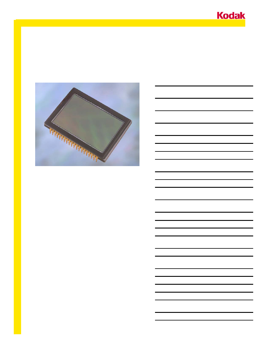
KODAK KAI-11000 Image Sensor
4008 (H) x 2672 (V) Interline
Transfer Progressive Scan CCD
Description
The Kodak KAI-11000 Image Sensor is a high-
performance 11-million pixel sensor designed for
professional digital still camera applications. The 9.0
µ
m square pixels with microlenses provide high
sensitivity and the large full well capacity results in
high dynamic range. The two high-speed outputs and
binning capabilities allow for 1-3 frames per second
(fps) video rate for the progressively scanned images.
The vertical overflow drain structure provides
antiblooming protection and enables electronic
shuttering for precise exposure control. Other features
include low dark current, negligible lag and low smear.
All parameters above are specified at T = 40*C
REVISION NO.: 3
EFFECTIVE DATE: June 3, 2003
Parameter Value
Architecture
Interline CCD;
Progressive Scan
Total Number of Pixels
4072 (H) x 2720 (V) =
approx. 11.1M
Number of Effective
Pixels
4032 (H) x 2688 (V) =
approx. 10.8M
Number of Active Pixels
4008 (H) x 2672 (V) =
approx. 10.7M
Number of Outputs
1 or 2
Pixel Size
9.0
µ
m (H) x 9.0
µ
m (V)
Imager Size
43.3mm (diagonal)
Chip Size
37.25mm (H) x
25.70mm (V)
Aspect Ratio
3:2
Saturation Signal
60,000 electrons
Quantum Efficiency
(KAI-11000M)
50%
Quantum Efficiency
(KAI-11000CM) RGB
34%, 37%, 42%
Output Sensitivity
13
µ
V/e
Total Noise
30 electrons
Dark Current
< 50 mV/s
Dark Current Doubling
Temperature
7 ∫C
Dynamic Range
66 dB
Charge Transfer
Efficiency
> 0.99999
Blooming Suppression
> 1000X
Smear
< -80 dB
Image Lag
< 10 electrons
Maximum Data Rate
28 MHz
Package
40-pin, CerDIP, 0.070" pin
spacing
Cover Glass
AR Coated