Document Outline
- Features
- Description
- Imaging
- Charge Transport and Sensing
- Package Configuration
- Pin Description
- Maximum Ratings
- DC Conditions
- AC Clock Level Conditions
- AC Timing
- Timing Diagram
- Clock Line Capacitance
- Image Specifications
- Defect Classification
- Quality Assurance and Reliability
- Ordering Information

KLI-5001G
Eastman Kodak Company - Image Sensor Solutions
For the most current information regarding this product:
Phone: (585) 722-4385 Fax: (585) 477-4947 Web: www.kodak.com/go/imagers E-mail: imagers@kodak.com
KLI-5001G
5000 Element Linear CCD Image Sensor
Performance Specification
Eastman Kodak Company
Image Sensor Solutions
Rochester, New York 14650-2010
Revision 8
May 21, 2002

KLI-5001G
Eastman Kodak Company - Image Sensor Solutions
For the most current information regarding this product:
Phone: (585) 722-4385 Fax: (585) 477-4947 Web: www.kodak.com/go/imagers E-mail: imagers@kodak.com
2
Revision No. 8
TABLE OF CONTENTS
Features....................................................................................................................... 3
Description................................................................................................................... 3
Imaging ........................................................................................................................ 4
Charge Transport and Sensing .................................................................................... 4
Package Configuration................................................................................................. 4
Pin Description............................................................................................................. 5
Maximum Ratings ........................................................................................................ 6
DC Conditions.............................................................................................................. 7
AC Clock Level Conditions........................................................................................... 8
AC Timing .................................................................................................................... 8
Timing Diagram............................................................................................................ 9
Clock Line Capacitance ............................................................................................... 10
Image Specifications.................................................................................................... 11
Defect Classification .................................................................................................... 12
Quality Assurance and Reliability................................................................................. 14
Ordering Information .................................................................................................... 15
FIGURES
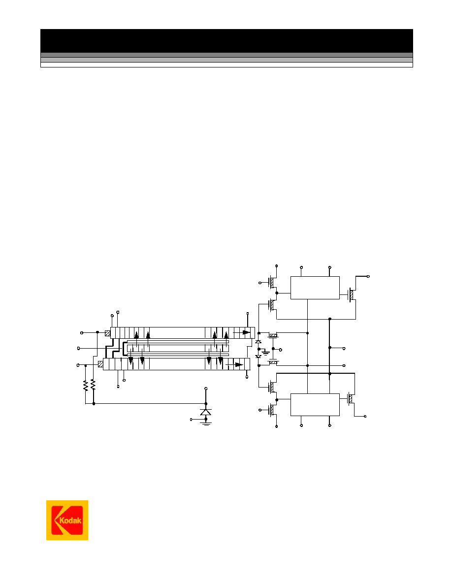
Figure 1 Imager Schematic....................................................................................... 3
Figure 2 Packaging Diagram..................................................................................... 4
Figure 3 Typical Output Bias/Buffer Circuit ............................................................... 7
Figure 4 Device Timing ............................................................................................. 9
Figure 5 Dark Signal Non-uniformity Definition ....................................................... 12
Figure 6 Defect Classification ................................................................................. 12
Figure 7 Device Responsivity.................................................................................. 13
Figure 8 Device Quantum Efficiency....................................................................... 13
Figure 9 Device Package Configuration.................................................................. 16
KLI-5001G
Eastman Kodak Company - Image Sensor Solutions
For the most current information regarding this product:
Phone: (585) 722-4385 Fax: (585) 477-4947 Web: www.kodak.com/go/imagers E-mail: imagers@kodak.com
3
Revision No. 8
Features
�
High resolution: 5000 pixels
� On-chip
Sample/Hold
�
Wide Dynamic Range
�
No Image Lag
�
High Charge Transfer Efficiency
�
Up to 2V peak-peak Output
�
Two-Phase Register Clocking
�
On-chip Dark Reference
Description
The KLI-5001G is a high resolution, linear array
designed for scanned imaging applications. This
device contains a row of 5000 active photoelements,
consisting of high performance 'pinned diodes' for
improved sensitivity, lower noise and elimination of
lag. Readout of the pixel data is accomplished through
the use of dual CCD shift registers, positioned on
either side of the detector array. The sensors are
positioned on 7�m centers with an associated 7�m
aperture spanning the length of the array.
The device architecture has on-chip correlated,
double-sampling circuitry. The device is manufactured
using NMOS, buried channel processing and utilize
dual layer polysilicon and dual layer metal
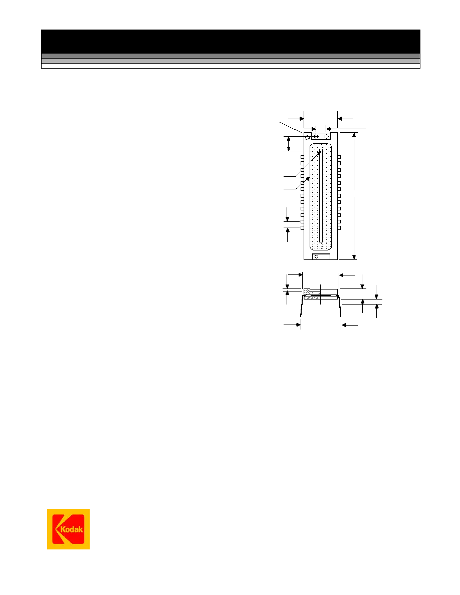
technologies. The die size is 36.00mm X 1.12mm and
the chip is housed in a 24-pin, 0.600" wide, dual in-line
package. Cover glass options include standard clear,
or multi-layer anti-reflection coated (MAR).
VIDA (18)
Photodiode Array
Register A
Register B
1 (3)
2 (22)
SG(2)
IG(23)
IDA(24)
IDB(1)
TG(6)
VRD (13)
R (11)
OG(12)
VG (10)
VSS (15)
C (9)
S (16)
VIDB (7)
Correlated Double
Sampling Circuitry
Correlated Double
Sampling Circuitry
VDD (19)
VSS (15)
C (9)
S (16)
PWL
(4,8,17)
NWL(21)
VG (10)
N/C 5,14,20
2 (22)
2.5
K
2.5
K
Figure 1 - Imager Schematic
KLI-5001G
Eastman Kodak Company - Image Sensor Solutions
For the most current information regarding this product:
Phone: (585) 722-4385 Fax: (585) 477-4947 Web: www.kodak.com/go/imagers E-mail: imagers@kodak.com
4
Revision No. 8
Imaging
During the integration period, an image is obtained by
collecting electrons generated by incident photons.
The charge stored in the photodiode array is a linear
function of the local exposure. The charge is isolated
from the CCD shift registers during this period by the
transfer gate TG, which is held at a barrier potential. At
the end of the integration period, the CCD register
clocking is stopped and the clock phase adjacent to
the photodiode,
1
, and the TG gate, are turned 'on'.
The charge is drained from the photosites through the
transfer gate and into the
1
region. The odd
photodiodes are drained to the 'A' register while the
even photodiodes are drained to the 'B' register. After
this transfer is complete, TG is turned 'off' once again,
isolating the two regions, while the current line is read
out and the next line is integrated.
Charge Transport and Sensing
The readout of the signal charge is accomplished by
two-phase, complementary clocking of the
1 and 2
gates. The data in both registers is clocked
simultaneously toward the output structures. The data
is transferred to the two output structures in parallel
format at the falling edge of the
2 clock. Resettable
floating diffusions are used for the charge-to-voltage
conversion while source followers provide buffering to
external connections. The potential change on the
floating diffusion is dependent on the amount of signal
charge and is given by
V
FD
=
Q/C
FD
. Prior to each
pixel output, the floating diffusion is returned to the RD
level by the reset clock,
R. The device incorporates
circuitry to implement correlated double-sampling
(CDS) of the output. This effectively removes kTC
noise and reduces in 1/f noise, as well as providing a
sampled and held output.
Package Configuration
-+
1.890
.018
0.577 .008
-+
-+
0.610 .006
0.198 .005
0.100 NOM
1
24
ELEMENT 5000
COVER GLASS
-+
0.200 .004
-+
GLASS THICKNESS
0.030 NOM.
0.665 .020
-+
0.155 .016
-+
0.050 NOM.
SEATING
OFFSET
ALL DIMENSIONS IN INCHES
Pin 1 Indicator
DETAILED PACKAGE DRAWINGS ARE AVAILABLE AT REQUEST
Figure 2 - Packaging Diagram
KLI-5001G
Eastman Kodak Company - Image Sensor Solutions
For the most current information regarding this product:
Phone: (585) 722-4385 Fax: (585) 477-4947 Web: www.kodak.com/go/imagers E-mail: imagers@kodak.com
5
Revision No. 8
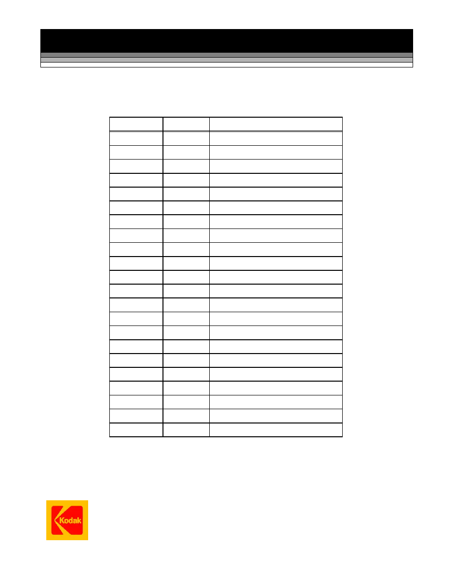
Pin Description
Pin Number
Symbol
Description
1
IDB
B Channel Input Diode (Test Pin)
2
SG
Signal Gate (Test Pin)
3
1
Phase 1 Register Clock
4 PWL Substrate
6
TG
PD-CCD Transfer Gate
7
VIDB
B Channel Output
8 PWL Substrate
9
C
Clamp Clock for CDS
10
VG
Load Gate Bias
11
R Reset
Clock
12
OG
Output Gate Bias
13
RD
Reset Drain Reference
15
VSS
Output Buffer Return
16
S
Sample Clock for CDS
17 PWL Substrate
18
VIDA
A Channel Output
19
VDD
Output Buffer Supply
21
NWL
Scavenger/Light Shield Bias
22
2
Phase 2 Register Clock
23
IG
Input Gate (Test Pin)
24
IDA
A Channel Input Diode (Test Pin)
5, 14, 20
No Connection