 | –≠–ª–µ–∫—Ç—Ä–æ–Ω–Ω—ã–π –∫–æ–º–ø–æ–Ω–µ–Ω—Ç: 80VA | –°–∫–∞—á–∞—Ç—å:  PDF PDF  ZIP ZIP |
Document Outline
- Table of Contents
- ispGDX80VA Data Sheet
- DC Electrical Characteristics
- AC Characteristics
- Pin Configuration: 100 TQFP
- Ordering Information

1
ispGDX
TM
80VA
In-System Programmable
3.3V Generic Digital Crosspoint
TM
Functional Block Diagram
Features
∑ IN-SYSTEM PROGRAMMABLE GENERIC DIGITAL
CROSSPOINT FAMILY
-- Advanced Architecture Addresses Programmable
PCB Interconnect, Bus Interface Integration and
Jumper/Switch Replacement
-- "Any Input to Any Output" Routing
-- Fixed HIGH or LOW Output Option for Jumper/DIP
Switch Emulation
-- Space-Saving PQFP and BGA Packaging
-- Dedicated IEEE 1149.1-Compliant Boundary Scan
Test
∑ HIGH PERFORMANCE E
2
CMOS
Æ
TECHNOLOGY
-- 3.3V Core Power Supply
-- 3.5ns Input-to-Output/3.5ns Clock-to-Output Delay
-- 250MHz Maximum Clock Frequency
-- TTL/3.3V/2.5V Compatible Input Thresholds and
Output Levels (Individually Programmable)
-- Low-Power: 16.5mA Quiescent Icc
-- 24mA I
OL
Drive with Programmable Slew Rate
Control Option
-- PCI Compatible Drive Capability
-- Schmitt Trigger Inputs for Noise Immunity
-- Electrically Erasable and Reprogrammable
-- Non-Volatile E
2
CMOS Technology
∑ ispGDXVTM OFFERS THE FOLLOWING ADVANTAGES
-- 3.3V In-System Programmable Using Boundary Scan
Test Access Port (TAP)
-- Change Interconnects in Seconds
∑ FLEXIBLE ARCHITECTURE
-- Combinatorial/Latched/Registered Inputs or Outputs
-- Individual I/O Tri-state Control with Polarity Control
-- Dedicated Clock/Clock Enable Input Pins (two) or
Programmable Clocks/Clock Enables from I/O Pins (20)
-- Single Level 4:1 Dynamic Path Selection (Tpd = 3.5ns)
-- Programmable Wide-MUX Cascade Feature
Supports up to 16:1 MUX
-- Programmable Pull-ups, Bus Hold Latch and Open
Drain on I/O Pins
-- Outputs Tri-state During Power-up ("Live Insertion"
Friendly)
∑ DESIGN SUPPORT THROUGH LATTICE'S ispGDX
DEVELOPMENT SOFTWARE
-- MS Windows or NT / PC-Based or Sun O/S
-- Easy Text-Based Design Entry
-- Automatic Signal Routing
-- Program up to 100 ISP Devices Concurrently
-- Simulator Netlist Generation for Easy Board-Level
Simulation
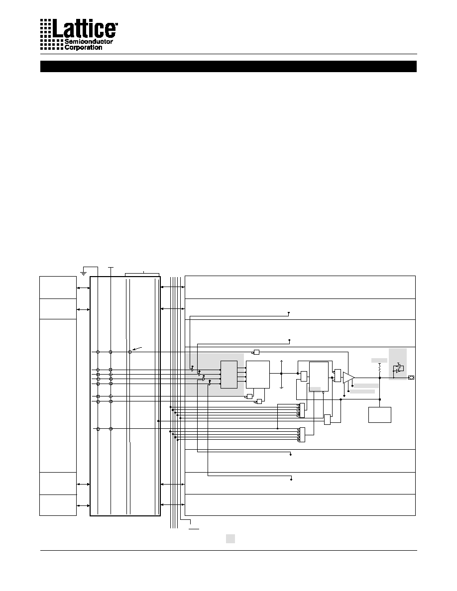
Global Routing
Pool
(GRP)
I/O
Cells
I/O Pins B
Boundary
Scan
Control
I/O
Cells
ISP
Control
I/O Pins
A
I/O Pins C
I/O Pins D
Description
The ispGDXVA architecture provides a family of fast,
flexible programmable devices to address a variety of
system-level digital signal routing and interface require-
ments including:
∑ Multi-Port Multiprocessor Interfaces
∑ Wide Data and Address Bus Multiplexing
(e.g. 16:1 High-Speed Bus MUX)
∑ Programmable Control Signal Routing
(e.g. Interrupts, DMAREQs, etc.)
∑ Board-Level PCB Signal Routing for Prototyping or
Programmable Bus Interfaces
The devices feature fast operation, with input-to-output
signal delays (Tpd) of 3.5ns and clock-to-output delays of
3.5ns.
The architecture of the devices consists of a series of
programmable I/O cells interconnected by a Global Rout-
ing Pool (GRP). All I/O pin inputs enter the GRP directly
or are registered or latched so they can be routed to the
required I/O outputs. I/O pin inputs are defined as four
sets (A,B,C,D) which have access to the four MUX inputs
gdx80va_02
Copyright © 2000 Lattice Semiconductor Corporation. All brand or product names are trademarks or registered trademarks of their respective holders. The specifications and information herein
are subject to change without notice.
LATTICE SEMICONDUCTOR CORP., 5555 Northeast Moore Ct., Hillsboro, Oregon 97124, U.S.A.
September 2000
Tel. (503) 268-8000; 1-800-LATTICE; FAX (503) 268-8037; http://www.latticesemi.com

2
Specifications
ispGDX80VA
Description (Continued)
found in each I/O cell. Each output has individual, pro-
grammable I/O tri-state control (OE), output latch clock
(CLK), clock enable (CLKEN), and two multiplexer con-
trol (MUX0 and MUX1) inputs. Polarity for these signals
is programmable for each I/O cell. The MUX0 and MUX1
inputs control a fast 4:1 MUX, allowing dynamic selection
of up to four signal sources for a given output. A wider
16:1 MUX can be implemented with the MUX expander
feature of each I/O and a propagation delay increase of
2.0ns. OE, CLK, CLKEN, and MUX0 and MUX1 inputs
can be driven directly from selected sets of I/O pins.
Optional dedicated clock input pins give minimum clock-
to-output delays. CLK and CLKEN share the same set of
I/O pins. CLKEN disables the register clock when
CLKEN = 0.
Through in-system programming, connections between
I/O pins and architectural features (latched or registered
inputs or outputs, output enable control, etc.) can be
defined. In keeping with its data path application focus,
the ispGDXVA devices contain no programmable logic
arrays. All input pins include Schmitt trigger buffers for
noise immunity. These connections are programmed
into the device using non-volatile E
2
CMOS technology.
Non-volatile technology means the device configuration
is saved even when the power is removed from the
device.
In addition, there are no pin-to-pin routing constraints for
1:1 or 1:n signal routing. That is,
any I/O pin configured
as an input can drive one or more I/O pins configured as
outputs.
The device pins also have the ability to set outputs to
fixed HIGH or LOW logic levels (Jumper or DIP Switch
mode). Device outputs are specified for 24mA sink and
12mA source current (at JEDEC LVTTL levels) and can
be tied together in parallel for greater drive. On the
ispGDXVA, each I/O pin is individually programmable for
3.3V or 2.5V output levels as described later. Program-
mable output slew rate control can be defined
independently for each I/O pin to reduce overall ground
bounce and switching noise.
All I/O pins are equipped with IEEE1149.1-compliant
Boundary Scan Test circuitry for enhanced testability. In
addition, in-system programming is supported through
the Test Access Port via a special set of private com-
mands.
The ispGDXVA I/Os are designed to withstand "live
insertion" system environments. The I/O buffers are
disabled during power-up and power-down cycles. When
designing for "live insertion," absolute maximum rating
conditions for the Vcc and I/O pins must still be met.
Table 1. ispGDXVA Family Members
ispGDXV/VA Device
ispGDX160V/VA
I/O Pins
160
I/O-OE Inputs*
40
I/O-CLK / CLKEN Inputs*
40
I/O-MUXsel1 Inputs*
40
I/O-MUXsel2 Inputs*
40
BSCAN Interface
4
RESET
1
Pin Count/Package
208-Pin PQFP
208-Ball fpBGA
272-Ball BGA
* The CLK/CLK_EN, OE, MUX0 and MUX1 terminals on each I/O cell can each be assigned to
25% of the I/Os.
** Global clock pins Y0, Y1, Y2 and Y3 are multiplexed with CLKEN0, CLKEN1, CLKEN2 and
CLKEN3 respectively in all devices.
TOE
1
Dedicated Clock Pins**
4
EPEN
1
80
20
20
20
20
4
1
100-Pin TQFP
1
2
1
240
60
60
60
60
4
1
388-Ball fpBGA
1
4
1
ispGDX80VA
ispGDX240VA
3
Specifications
ispGDX80VA
Architecture
The ispGDXVA architecture is different from traditional
PLD architectures, in keeping with its unique application
focus. The block diagram is shown below. The program-
mable interconnect consists of a single Global Routing
Pool (GRP). Unlike ispLSI devices, there are no pro-
grammable logic arrays on the device. Control signals for
OEs, Clocks/Clock Enables and MUX Controls must
come from designated sets of I/O pins. The polarity of
these signals can be independently programmed in each
I/O cell.
Each I/O cell drives a unique pin. The OE control for each
I/O pin is independent and may be driven via the GRP by
one of the designated I/O pins (I/O-OE set). The I/O-OE
set consists of 25% of the total I/O pins. Boundary Scan
test is supported by dedicated registers at each I/O pin.
In-system programming is accomplished through the
standard Boundary Scan protocol.
The various I/O pin sets are also shown in the block
diagram below. The A, B, C, and D I/O pins are grouped
together with one group per side.
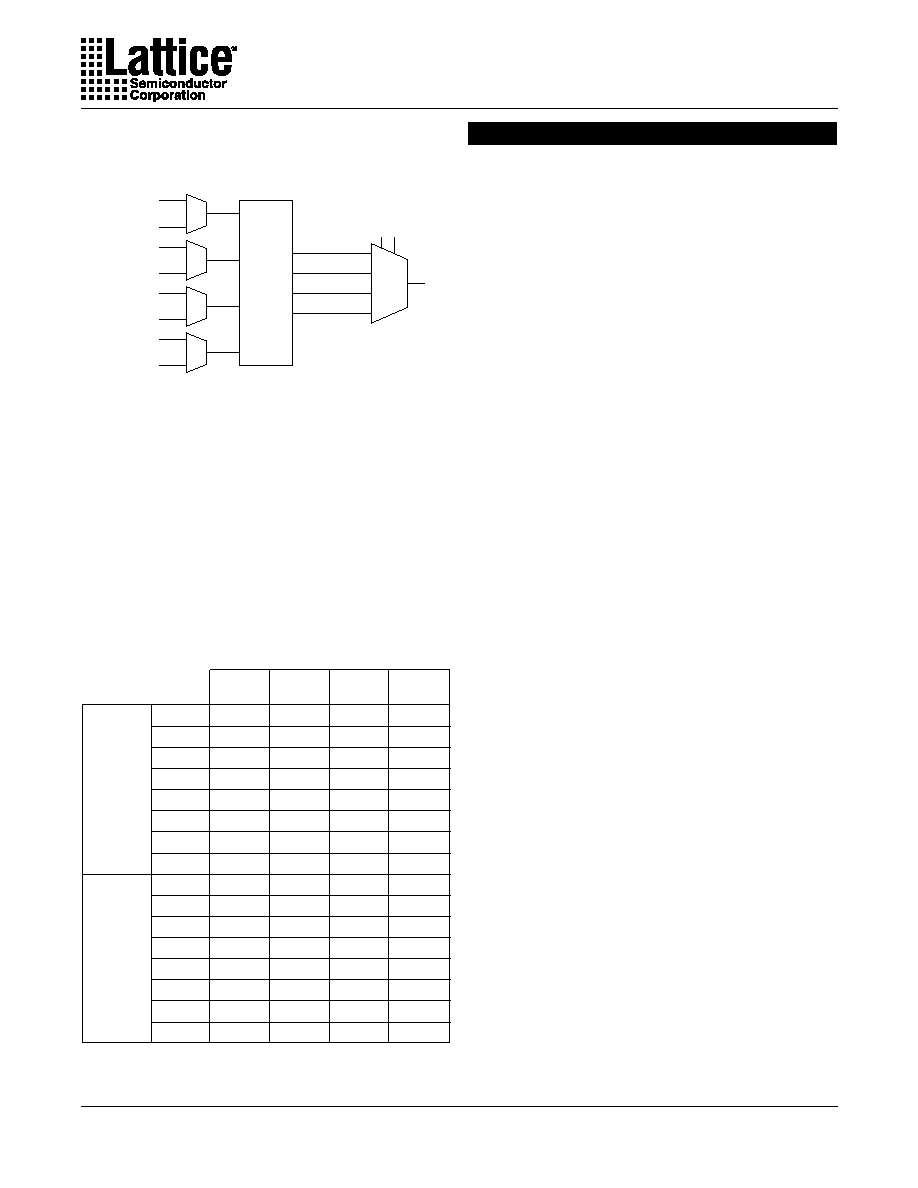
I/O Architecture
Each I/O cell contains a 4:1 dynamic MUX controlled by
two select lines as well as a 4x4 crossbar switch con-
trolled by software for increased routing flexiability (Figure
1). The four data inputs to the MUX (called M0, M1, M2,
and M3) come from I/O signals in the GRP and/or
adjacent I/O cells. Each MUX data input can access one
quarter of the total I/Os. For example, in an 80-I/O
ispGDXVA, each data input can connect to one of 20 I/O
pins. MUX0 and MUX1 can be driven by designated I/O
pins called MUXsel1 and MUXsel2. Each MUXsel input
covers 25% of the total I/O pins (e.g. 20 out of 80). MUX0
and MUX1 can be driven from either MUXsel1 or MUXsel2.
Figure 1. ispGDXVA I/O Cell and GRP Detail (80 I/O Device)
I/OCell 0
I/O Cell 1
I/O Cell 38
I/O Cell 39
40 I/O Cells
Boundary
Scan Cell
Bypass Option
I/O Cell N
Register
or Latch
I/O
Pin
Prog.
Pull-up
(VCCIO)
Prog. Slew Rate
D
A
B
CLK
Reset
Q
4-to-1 MUX
80 Input GRP
Inputs Vertical
Outputs Horizontal
I/O Cell 79
I/O Cell 78
I/O Cell 41
M0
I/O Group A
I/O Group B
I/O Group C
I/O Group D
M1
4x4
Crossbar
Switch
M2
M3
MUX1
MUX0
Global
Reset
I/O Cell 40
∑ ∑ ∑ ∑ ∑ ∑
∑
∑
∑
40 I/O Cells
ispGDXVA architecture enhancements over ispGDX (5V)
∑
∑
∑
∑
∑
∑
E
2
CMOS
Programmable
Interconnect
Logic "0" Logic "1"
80 I/O Inputs
C
R
Y0-Y3
Global
Clocks /
Clock_Enables
Prog.
Bus Hold
Latch
CLK_EN
From MUX Outputs
of 2 Adjacent I/O Cells
From MUX Outputs
of 2 Adjacent I/O Cells
To 2 Adjacent
I/O Cells above
To 2 Adjacent
I/O Cells below
Prog. Open Drain
2.5V/3.3V Output
∑
∑
∑
N+1
N+2
N-1
N-2

4
Specifications
ispGDX80VA
Flexible mapping of MUXsel
x
to MUX
x
allows the user to
change the MUX select assignment after the ispGDXVA
device has been soldered to the board. Figure 1 shows
that the I/O cell can accept (by programming the appro-
priate fuses) inputs from the MUX outputs of four adjacent
I/O cells, two above and two below. This enables cascad-
ing of the MUXes to enable wider (up to 16:1) MUX
implementations.
The I/O cell also includes a programmable flow-through
latch or register that can be placed in the input or output
path and bypassed for combinatorial outputs. As shown
in Figure 1, when the input control MUX of the register/
latch selects the "A" path, the register/latch gets its inputs
from the 4:1 MUX and drives the I/O output. When
selecting the "B" path, the register/latch is directly driven
by the I/O input while its output feeds the GRP. The
programmable polarity Clock to the latch or register can
be connected to any I/O in the I/O-CLK/CLKEN set (one-
quarter of total I/Os) or to one of the dedicated clock input
pins (Y
x
). The programmable polarity Clock Enable input
to the register can be programmed to connect to any of
the I/O-CLK/CLKEN input pin set or to the global clock
enable inputs (CLKEN
x
). Use of the dedicated clock
inputs gives minimum clock-to-output delays and mini-
mizes delay variation with fanout. Combinatorial output
mode may be implemented by a dedicated architecture
bit and bypass MUX. I/O cell output polarity can be
programmed as active high or active low.
MUX Expander Using Adjacent I/O Cells
The ispGDXVA allows adjacent I/O cell MUXes to be
cascaded to form wider input MUXes (up to 16 x 1)
without incurring an additional full Tpd penalty. However,
there are certain dependencies on the locality of the
adjacent MUXes when used along with direct MUX
inputs.
Adjacent I/O Cells
Expansion inputs MUXOUT[n-2], MUXOUT[n-1],
MUXOUT[n+1], and MUXOUT[n+2] are fuse-selectable
for each I/O cell MUX. These expansion inputs share the
same path as the standard A, B, C and D MUX inputs, and
allow adjacent I/O cell outputs to be directly connected
without passing through the global routing pool. The
relationship between the [N+i] adjacent cells and A, B, C
and D inputs will vary depending on where the I/O cell is
located on the physical die. The I/O cells can be grouped
into "normal" and "reflected" I/O cells or I/O "hemi-
spheres." These are defined as:
I/O MUX Operation
MUX1
MUX0
Data Input Selected
0
0
M0
0
1
M1
1
1
M2
1
0
M3
Device
Normal I/O Cells
Reflected I/O Cells
B9-B0, A19-A0,
D19-D10
B10-B19, C0-C19,
D0-D9
B19-B0, A39-A0,
D39-D20
B20-B39, C0-C39,
D0-D19
ispGDX80VA
ispGDX160V/VA
ispGDX240VA
B29-B0, A59-A0,
D59-D30
B30-B59, C0-C59,
D0-D29
Table 2 shows the relationship between adjacent I/O
cells as well as their relationship to direct MUX inputs.
Note that the MUX expansion is circular and that I/O cell
B10, for example, draws on I/Os B9 and B8, as well as
B11 and B12, even though they are in different hemi-
spheres of the physical die. Table 2 shows some typical
cases and all boundary cases. All other cells can be
extrapolated from the pattern shown in the table.
D10
D9
B9
B10
A0
A19
C19
C0
D19
B0
D0
B19
I/O cell 0
I/O cell 79
I/O cell 39
I/O cell 40
I/O cell index increases in this direction
I/O cell index increases in this direction
Figure 2. I/O Hemisphere Configuration of
ispGDX80VA
Direct and Expander Input Routing
Table 2 also illustrates the routing of MUX direct inputs
that are accessible when using adjacent I/O cells as
inputs. Take I/O cell D13 as an example, which is also
shown in Figure 3.
5
Specifications
ispGDX80VA
B10
B11
B12
B13
D6
D7
D8
D9
D10
D11
D12
D13
B6
B7
B8
B9
B12
B13
B14
B15
D8
D9
D10
D11
D8
D9
D10
D11
B4
B5
B6
B7
B11
B12
B13
B14
D7
D8
D9
D10
D9
D10
D11
D12
B5
B6
B7
B8
B9
B10
B11
B12
D5
D6
D7
D8
D11
D12
D13
D14
B7
B8
B9
B10
B8
B9
B10
B11
D4
D5
D6
D7
D12
D13
D14
D15
B8
B9
B10
B11
Data D/
MUXOUT
Data C/
MUXOUT
Data B/
MUXOUT
Data A/
MUXOUT
Reflected
I/O Cells
Normal
I/O Cells
Table 2. Adjacent I/O Cells (Mapping of
ispGDX80VA)
It can be seen from Figure 3 that if the D11 adjacent I/O
cell is used, the I/O group "A" input is no longer available
as a direct MUX input.
The ispGDXVA can implement MUXes up to 16 bits wide
in a single level of logic, but care must be taken when
combining adjacent I/O cell outputs with direct MUX
inputs. Any particular combination of adjacent I/O cells as
MUX inputs will dictate what I/O groups (A, B, C or D) can
be routed to the remaining inputs. By properly choosing
the adjacent I/O cells, all of the MUX inputs can be
utilized.
S0
S1
4 x 4
Crossbar
Switch
.m0
.m1
.m2
.m3
D13
I/O Group A
D11 MUX Out
I/O Group B
D12 MUX Out
I/O Group C
D14 MUX Out
I/O Group D
D15 MUX Out
ispGDX80VA I/O Cell
Figure 3. Adjacent I/O Cells vs. Direct Input Path for
ispGDX80VA, I/O D13
Special Features
Slew Rate Control
All output buffers contain a programmable slew rate
control that provides software-selectable slew rate op-
tions.
Open Drain Control
All output buffers provide a programmable Open-Drain
option which allows the user to drive system level reset,
interrupt and enable/disable lines directly without the
need for an off-chip Open-Drain or Open-Collector buffer.
Wire-OR logic functions can be performed at the printed
circuit board level.
Pull-up Resistor
All pins have a programmable active pull-up. A typical
resistor value for the pull-up ranges from 50k
to 80k
.
Output Latch (Bus Hold)
All pins have a programmable circuit that weakly holds
the previously driven state when all drivers connected to
the pin (including the pin's output driver as well as any
other devices connected to the pin by external bus) are
tristated.
User-Programmable I/Os
The ispGDX80VA features user-programmable
I/Os supporting either 3.3V or 2.5V output voltage level
options. The ispGDX80VA uses a VCCIO pin to provide
the 2.5V reference voltage when used.
PCI Compatible Drive Capability
The ispGDX80VA supports PCI compatible drive capa-
bility for all I/Os.