
GAL16V8Z
GAL16V8ZD
Zero Power E
2
CMOS PLD
1
DESCRIPTION
GAL16V8Z
GAL16V8ZD
Top View
DIP/SOIC
GAL
16V8Z
16V8ZD
I/O/Q
I/O/Q
1 9
I/DPP
I
I
I
4
1 1
1 8
3
6
9
1 6
I
I/O/Q
I/O/Q
I/O/Q
1 3
1 4
8
1
I/C
L
K
I
I
GN
D
I/O
/Q
I
I/O
E
Vc
c
I/O
/Q
I/O
/Q
I
I/ O/ Q
I/ O/ Q
I/ O/ Q
I/ O/ Q
G N D
I/ O/ Q
I/ O/ Q
I/ O/ Q
I/ O/ Q
I/C L K
I
I
I/D P P
V c c
I
I
I
I
I /O E
1
2 0
1 5
5
1 0
1 1
2
3
4
6
7
8
9
12
13
14
16
17
18
19
I/CLK
I
I/O/Q
I
I/O/Q
I/DPP
I/O/Q
I
I/O/Q
I
I/O/Q
I
I/O/Q
I
I/O/Q
I
I/O/Q
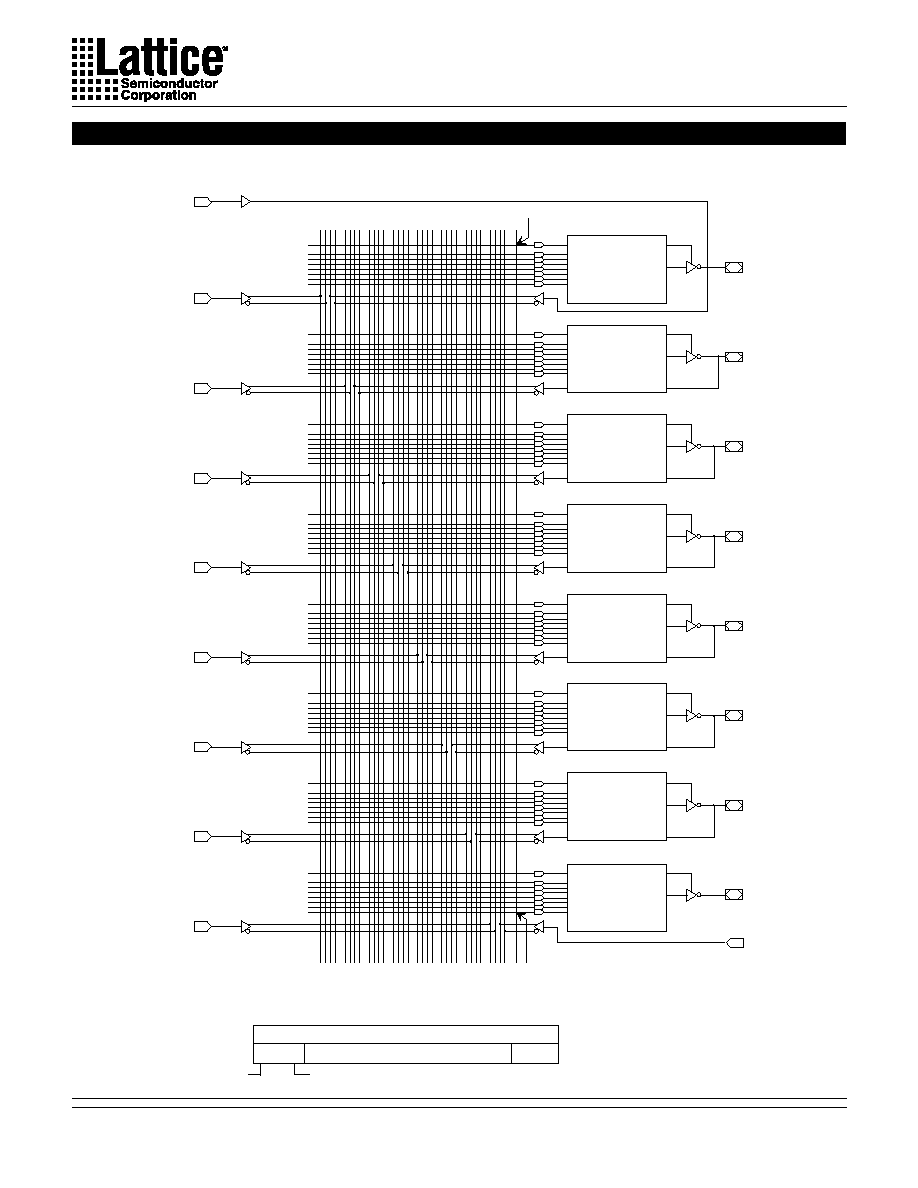
CLK
8
8
8
8
8
8
8
8
OE
OLMC
OLMC
OLMC
OLMC
OLMC
OLMC
OLMC
OLMC
PROGRAMMABLE
AND-ARRAY
(64 X 32)
I/OE
Copyright � 1997 Lattice Semiconductor Corp. All brand or product names are trademarks or registered trademarks of their respective holders. The specifications and information herein are subject
to change without notice.
LATTICE SEMICONDUCTOR CORP., 5555 Northeast Moore Ct., Hillsboro, Oregon 97124, U.S.A.
December 1997
Tel. (503) 268-8000; 1-800-LATTICE; FAX (503) 268-8556; http://www.latticesemi.com
PLCC
16v8zzd_03
Features
� ZERO POWER E
2
CMOS TECHNOLOGY
-- 100
�
A Standby Current
-- Input Transition Detection on GAL16V8Z
-- Dedicated Power-down Pin on GAL16V8ZD
-- Input and Output Latching During Power Down
� HIGH PERFORMANCE E
2
CMOS TECHNOLOGY
-- 12 ns Maximum Propagation Delay
-- Fmax = 83.3 MHz
-- 8 ns Maximum from Clock Input to Data Output
-- TTL Compatible 16 mA Output Drive
-- UltraMOS
�
Advanced CMOS Technology
� E
2
CELL TECHNOLOGY
-- Reconfigurable Logic
-- Reprogrammable Cells
-- 100% Tested/100% Yields
-- High Speed Electrical Erasure (<100ms)
-- 20 Year Data Retention
� EIGHT OUTPUT LOGIC MACROCELLS
-- Maximum Flexibility for Complex Logic Designs
-- Programmable Output Polarity
-- Architecturally Similar to Standard GAL16V8
� PRELOAD AND POWER-ON RESET OF ALL REGISTERS
-- 100% Functional Testability
� APPLICATIONS INCLUDE:
-- Battery Powered Systems
-- DMA Control
-- State Machine Control
-- High Speed Graphics Processing
� ELECTRONIC SIGNATURE FOR IDENTIFICATION
Description
The GAL16V8Z and GAL16V8ZD, at 100
�
A standby current and
12ns propagation delay provides the highest speed and lowest
power combination PLD available in the market. The GAL16V8Z/
ZD is manufactured using Lattice Semiconductor's advanced zero
power E
2
CMOS process, which combines CMOS with Electrically
Erasable (E
2
) floating gate technology.
The GAL16V8Z uses Input Transition Detection (ITD) to put the
device in standby mode and is capable of emulating the full func-
tionality of the standard GAL16V8. The GAL16V8ZD utilizes a
dedicated power-down pin (DPP) to put the device in standby mode.
It has 15 inputs available to the AND array.
Unique test circuitry and reprogrammable cells allow complete AC,
DC, and functional testing during manufacture. As a result,
Lattice Semiconductor delivers 100% field programmability and
functionality of all GAL products. In addition, 100 erase/write cycles
and data retention in excess of 20 years are specified.
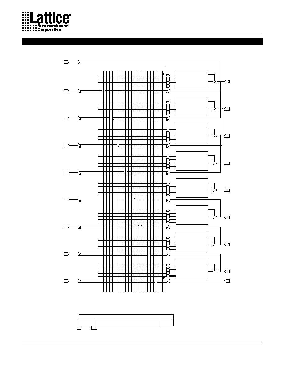
Functional Block Diagram
Pin Configuration
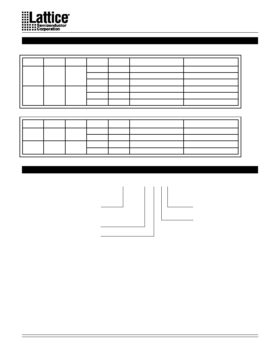
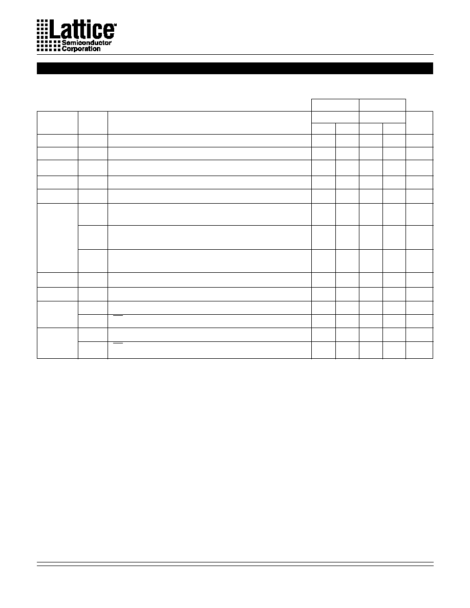
Specifications
GAL16V8Z
GAL16V8ZD
2
Tpd (ns)
Tsu (ns)
Tco (ns)
Icc (mA)
Isb (
�
A)
Ordering #
Package
12
10
8
55
100
GAL16V8Z-12QP
20-Pin Plastic DIP
55
100
GAL16V8Z-12QJ
20-Lead PLCC
55
100
GAL16V8Z-12QS
20-Lead SOIC
15
15
10
55
100
GAL16V8Z-15QP
20-Pin Plastic DIP
55
100
GAL16V8Z-15QJ
20-Lead PLCC
55
100
GAL16V8Z-15QS
20-Lead SOIC
Tpd (ns)
Tsu (ns)
Tco (ns)
Icc (mA)
Isb (
�
A)
Ordering #
Package
12
10
8
55
100
GAL16V8ZD-12QP
20-Pin Plastic DIP
55
100
GAL16V8ZD-12QJ
20-Lead PLCC
15
15
10
55
100
GAL16V8ZD-15QP
20-Pin Plastic DIP
55
100
GAL16V8ZD-15QJ
20-Lead PLCC
Blank = Commercial
Grade
Package
Active Power
Q = Quarter Power
XXXXXXXX
XX
X
X X
Device Name
_
P = Plastic DIP
J = PLCC
S = SOIC
GAL16V8Z (Zero Power ITD)
GAL16V8ZD (Zero Power DPP)
Speed (ns)
GAL16V8ZD: Commercial Grade Specifications
GAL16V8Z/ZD Ordering Information
GAL16V8Z: Commercial Grade Specifications
Part Number Description
Specifications
GAL16V8Z
GAL16V8ZD
3
The following discussion pertains to configuring the output logic
macrocell. It should be noted that actual implementation is accom-
plished by development software/hardware and is completely trans-
parent to the user.
There are three global OLMC configuration modes possible:
simple, complex, and registered. Details of each of these modes
is illustrated in the following pages. Two global bits, SYN and AC0,
control the mode configuration for all macrocells. The XOR bit of
each macrocell controls the polarity of the output in any of the three
modes, while the AC1 bit of each of the macrocells controls the in-
put/output configuration. These two global and 16 individual archi-
tecture bits define all possible configurations in a GAL16V8Z/ZD.
The information given on these architecture bits is only to give a
better understanding of the device. Compiler software will trans-
parently set these architecture bits from the pin definitions, so the
user should not need to directly manipulate these architecture bits.
Software compilers support the three different global OLMC modes
as different device types. Most compilers also have the ability to
automatically select the device type, generally based on the register
usage and output enable (OE) usage. Register usage on the device
forces the software to choose the registered mode. All combina-
torial outputs with OE controlled by the product term will force the
software to choose the complex mode. The software will choose
the simple mode only when all outputs are dedicated combinatorial
without OE control. For further details, refer to the compiler soft-
ware manuals.
When using compiler software to configure the device, the user
must pay special attention to the following restrictions in each mode.
In registered mode pin 1 and pin 11 are permanently configured
as clock and output enable, respectively. These pins cannot be con-
figured as dedicated inputs in the registered mode.
In complex mode pin 1 and pin 11 become dedicated inputs and
use the feedback paths of pin 19 and pin 12 respectively. Because
of this feedback path usage, pin 19 and pin 12 do not have the
feedback option in this mode.
In simple mode all feedback paths of the output pins are routed
via the adjacent pins. In doing so, the two inner most pins ( pins
15 and 16) will not have the feedback option as these pins are
always configured as dedicated combinatorial output.
When using the standard GAL16V8 JEDEC fuse pattern generated
by the logic compilers for the GAL16V8ZD, special attention must
be given to pin 4 (DPP) to make sure that it is not used as one of
the functional inputs.
Output Logic Macrocell (OLMC)
Compiler Support for OLMC

Specifications
GAL16V8Z
GAL16V8ZD
4
In the Registered mode, macrocells are configured as dedicated
registered outputs or as I/O functions.
Architecture configurations available in this mode are similar to
the common 16R8 and 16RP4 devices with various permutations
of polarity, I/O and register placement.
All registered macrocells share common clock and output enable
control pins. Any macrocell can be configured as registered or
I/O. Up to eight registers or up to eight I/Os are possible in this
mode. Dedicated input or output functions can be implemented
as subsets of the I/O function.
Registered outputs have eight product terms per output. I/Os have
seven product terms per output.
Pin 4 is used as dedicated power-down pin on GAL16V8ZD. It
cannot be used as functional input.
The JEDEC fuse numbers, including the User Electronic Signature
(UES) fuses and the Product Term Disable (PTD) fuses, are
shown on the logic diagram on the following page.
Combinatorial Configuration for Registered Mode
- SYN=0.
- AC0=1.
- XOR=0 defines Active Low Output.
- XOR=1 defines Active High Output.
- AC1=1 defines this output configuration.
- Pin 1 & Pin 11 are permanently configured as CLK &
OE
for registered output configuration.
Registered Configuration for Registered Mode
- SYN=0.
- AC0=1.
- XOR=0 defines Active Low Output.
- XOR=1 defines Active High Output.
- AC1=0 defines this output configuration.
- Pin 1 controls common CLK for the registered outputs.
- Pin 11 controls common
OE
for the registered outputs.
- Pin 1 & Pin 11 are permanently configured as CLK &
OE
for registered output configuration.
Note: The development software configures all of the architecture control bits and checks for proper pin usage automatically.
D
Q
Q
CLK
OE
XOR
XOR
Registered Mode

Specifications
GAL16V8Z
GAL16V8ZD
5
DIP, SOIC & PLCC Package Pinouts
MSB LSB
64-USER ELECTRONIC SIGNATURE FUSES
2056, 2057, .... .... 2118, 2119
Byte7 Byte6 .... .... Byte1 Byte0
SYN-2192
AC0-2193
* Note: Input not available on GAL16V8ZD
*
1
2
3
4
5
6
7
8
9
11
12
13
14
15
16
17
18
0000
0224
0256
0480
0512
0736
0768
0992
1024
1248
1280
1504
1536
1760
1792
2016
19
XOR-2048
AC1-2120
XOR-2049
AC1-2121
XOR-2050
AC1-2122
XOR-2051
AC1-2123
XOR-2052
AC1-2124
XOR-2053
AC1-2125
XOR-2054
AC1-2126
XOR-2055
AC1-2127
28
24
20
16
12
8
4
0
PTD
2128
2191
OE
OLMC
OLMC
OLMC
OLMC
OLMC
OLMC
OLMC
OLMC
Registered Mode Logic Diagram

Specifications
GAL16V8Z
GAL16V8ZD
6
In the Complex mode, macrocells are configured as output only or
I/O functions.
Architecture configurations available in this mode are similar to the
common 16L8 and 16P8 devices with programmable polarity in
each macrocell.
Up to six I/Os are possible in this mode. Dedicated inputs or outputs
can be implemented as subsets of the I/O function. The two outer
most macrocells (pins 12 & 19) do not have input capability. De-
signs requiring eight I/Os can be implemented in the Registered
mode.
All macrocells have seven product terms per output. One product
term is used for programmable output enable control. Pins 1 and
11 are always available as data inputs into the AND array.
Pin 4 is used as dedicated power-down pin on GAL16V8ZD. It can-
not be used as functional input.
The JEDEC fuse numbers including the UES fuses and PTD fuses
are shown on the logic diagram on the following page.
Note: The development software configures all of the architecture control bits and checks for proper pin usage automatically.
Combinatorial I/O Configuration for Complex Mode
- SYN=1.
- AC0=1.
- XOR=0 defines Active Low Output.
- XOR=1 defines Active High Output.
- AC1 has no effect on this mode.
- Pin 13 through Pin 18 are configured to this function.
Combinatorial Output Configuration for Complex Mode
- SYN=1.
- AC0=1.
- XOR=0 defines Active Low Output.
- XOR=1 defines Active High Output.
- AC1 has no effect on this mode.
- Pin 12 and Pin 19 are configured to this
function.
XOR
XOR
Complex Mode
Specifications
GAL16V8Z
GAL16V8ZD
7
DIP, SOIC & PLCC Package Pinouts
MSB LSB
64-USER ELECTRONIC SIGNATURE FUSES
2056, 2057, .... .... 2118, 2119
Byte7 Byte6 .... .... Byte1 Byte0
SYN-2192
AC0-2193
*
* Note: Input not available on GAL16V8ZD
0000
0224
0256
0480
0512
0736
0768
0992
1024
1248
1280
1504
1536
1760
1792
2016
PTD
2128
2191
11
12
13
14
15
16
17
18
19
1
2
3
4
5
6
7
8
9
OLMC
OLMC
OLMC
OLMC
OLMC
OLMC
XOR-2055
AC1-2127
XOR-2054
AC1-2126
XOR-2053
AC1-2125
XOR-2052
AC1-2124
XOR-2051
AC1-2123
XOR-2050
AC1-2122
XOR-2049
AC1-2121
XOR-2048
AC1-2120
OLMC
OLMC
28
24
20
16
12
8
4
0
Complex Mode Logic Diagram
Specifications
GAL16V8Z
GAL16V8ZD
8
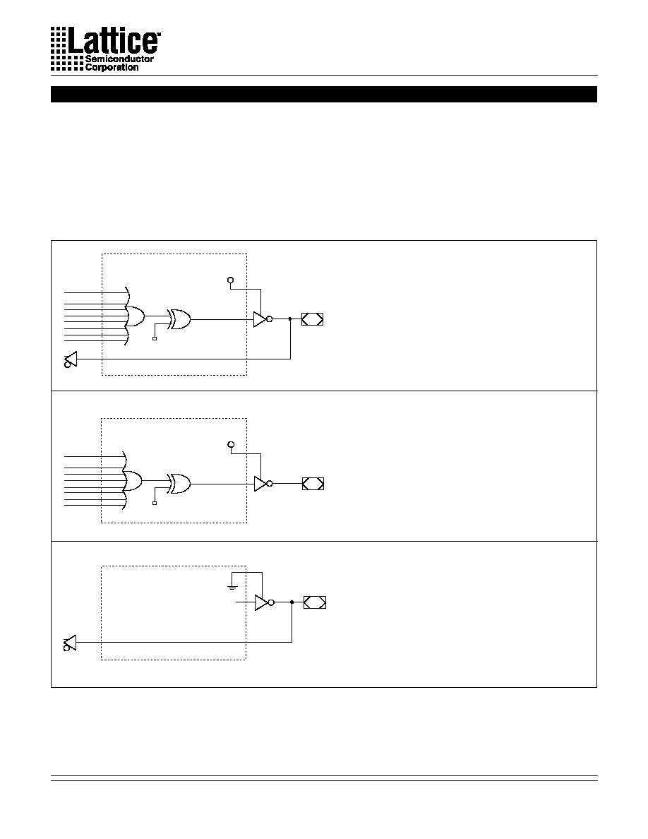
Combinatorial Output with Feedback Configuration
for Simple Mode
- SYN=1.
- AC0=0.
- XOR=0 defines Active Low Output.
- XOR=1 defines Active High Output.
- AC1=0 defines this configuration.
- All OLMC except pins 15 & 16 can be configured to
this function.
Combinatorial Output Configuration for Simple Mode
- SYN=1.
- AC0=0.
- XOR=0 defines Active Low Output.
- XOR=1 defines Active High Output.
- AC1=0 defines this configuration.
- Pins 15 & 16 are permanently configured to this
function.
Dedicated Input Configuration for Simple Mode
- SYN=1.
- AC0=0.
- XOR=0 defines Active Low Output.
- XOR=1 defines Active High Output.
- AC1=1 defines this configuration.
- All OLMC except pins 15 & 16 can be configured to
this function.
Note: The development software configures all of the architecture control bits and checks for proper pin usage automatically.
In the Simple mode, macrocells are configured as dedicated inputs
or as dedicated, always active, combinatorial outputs.
Architecture configurations available in this mode are similar to the
common 10L8 and 12P6 devices with many permutations of ge-
neric output polarity or input choices.
All outputs in the simple mode have a maximum of eight porduct
terms that can control the logic. In addition, each output has pro-
grammable polarity.
Pins 1 and 11 are always available as data inputs into the AND
array. The center two macrocells (pins 15 & 16) cannot be used
in the input configuration.
Pin 4 is used as dedicated power-down pin on GAL16V8ZD. It can-
not be used as functional input.
The JEDEC fuse numbers including the UES fuses and PTD fuses
are shown on the logic diagram.
Vcc
XOR
Vcc
XOR
Simple Mode
Specifications
GAL16V8Z
GAL16V8ZD
9
DIP, SOIC & PLCC Package Pinouts
MSB LSB
64-USER ELECTRONIC SIGNATURE FUSES
2056, 2057, .... .... 2118, 2119
Byte7 Byte6 .... .... Byte1 Byte0
SYN-2192
AC0-2193
*
* Note: Input not available on GAL16V8ZD
1
11
12
13
14
15
16
17
18
19
2
3
4
5
6
7
9
0000
0224
0256
0480
0512
0736
0768
0992
1024
1248
1280
1504
1536
1760
1792
2016
PTD
2128
2191
8
XOR-2048
AC1-2120
OLMC
XOR-2049
AC1-2121
XOR-2050
AC1-2122
XOR-2051
AC1-2123
XOR-2052
AC1-2124
XOR-2053
AC1-2125
XOR-2054
AC1-2126
XOR-2055
AC1-2127
OLMC
OLMC
OLMC
OLMC
OLMC
OLMC
OLMC
28
24
20
16
12
8
4
0
Simple Mode Logic Diagram

Specifications
GAL16V8Z
GAL16V8ZD
10
COMMERCIAL
I
SB
Stand-by Power
V
IL
= GND V
IH
= Vcc Outputs Open
Z-12/-15
--
50
100
�
A
Supply Current
ZD-12/-15
I
CC
Operating Power
V
IL
= 0.5V V
IH
= 3.0V
Z-12/-15
--
--
55
mA
Supply Current
f
toggle
= 15 MHz Outputs Open
ZD-12/-15
Recommended Operating Conditions
Commercial Devices:
Ambient Temperature (T
A
) ............................... 0 to 75
�
C
Supply voltage (V
CC
)
with Respect to Ground ..................... +4.75 to +5.25V
Absolute Maximum Ratings
(1)
Supply voltage V
CC
........................................ �.5 to +7V
Input voltage applied .......................... �2.5 to V
CC
+1.0V
Off-state output voltage applied ......... �2.5 to V
CC
+1.0V
Storage Temperature ................................ �65 to 150
�
C
Ambient Temperature with
Power Applied ........................................... �55 to 125
�
C
1. Stresses above those listed under the "Absolute Maximum
Ratings" may cause permanent damage to the device. These
are stress only ratings and functional operation of the device
at these or at any other conditions above those indicated in
the operational sections of this specification is not implied
(while programming, follow the programming specifications).
SYMBOL
PARAMETER
MAXIMUM*
UNITS
TEST CONDITIONS
C
I
Input Capacitance
10
pF
V
CC
= 5.0V, V
I
= 2.0V
C
I/O
I/O Capacitance
10
pF
V
CC
= 5.0V, V
I/O
= 2.0V
*Characterized but not 100% tested.
SYMBOL
PARAMETER
CONDITION
MIN.
TYP.
2
MAX.
UNITS
V
IL
Input Low Voltage
Vss � 0.5
--
0.8
V
V
IH
Input High Voltage
2.0
--
Vcc+1
V
I
IL
Input or I/O Low Leakage Current
0V
V
IN
V
IL
(MAX.)
--
--
�
10
�
A
I
IH
Input or I/O High Leakage Current
3.5V
V
IN
V
CC
--
--
10
�
A
V
OL
Output Low Voltage
I
OL
= MAX. Vin = V
IL
or V
IH
--
--
0.5
V
V
OH
Output High Voltage
I
OH
= MAX. Vin = V
IL
or V
IH
2.4
--
--
V
I
OH
= -100
�
A Vin = V
IL
or V
IH
Vcc-1
--
--
V
I
OL
Low Level Output Current
--
--
16
mA
I
OH
High Level Output Current
--
--
�3.2
mA
I
OS
1
Output Short Circuit Current
V
CC
= 5V
V
OUT
= 0.5V
T
A
= 25
�
C
�30
--
�150
mA
1) One output at a time for a maximum duration of one second. Vout = 0.5V was selected to avoid test problems by tester ground
degradation. Characterized but not 100% tested.
2) Typical values are at Vcc = 5V and T
A
= 25
�
C
DC Electrical Characteristics
Over Recommended Operating Conditions (Unless Otherwise Specified)
Capacitance (T
A
= 25
�
C, f = 1.0 MHz)

Specifications
GAL16V8Z
GAL16V8ZD
11
Specifications
GAL16V8Z
t
pd
A
Input or I/O to Combinational Output
3
12
3
15
ns
t
co
A
Clock to Output Delay
2
8
2
10
ns
t
cf
2
--
Clock to Feedback Delay
--
6
--
7
ns
t
su
--
Setup Time, Input or Feedback before Clock
10
--
15
--
ns
t
h
--
Hold Time, Input or Feedback after Clock
0
--
0
--
ns
A
Maximum Clock Frequency with
55
--
40
--
MHz
External Feedback, 1/(tsu + tco)
f
max
3
A
Maximum Clock Frequency with
62.5
--
45.5
--
MHz
Internal Feedback, 1/(tsu + tcf)
A
Maximum Clock Frequency with
83.3
--
62.5
--
MHz
No Feedback
t
wh
--
Clock Pulse Duration, High
6
--
8
--
ns
t
wl
--
Clock Pulse Duration, Low
6
--
8
--
ns
t
en
B
Input or I/O to Output Enabled
--
12
--
15
ns
B
OE to Output Enabled
--
12
--
15
ns
t
dis
C
Input or I/O to Output Disabled
--
15
--
15
ns
C
OE to Output DIsabled
--
12
--
15
ns
t
as
--
Last Active Input to Standby
60
140
50
150
ns
t
sa
4
--
Standby to Active Output
6
13
5
15
ns
PARAMETER
UNITS
-15
MIN. MAX.
TEST
COND
1
.
DESCRIPTION
-12
MIN. MAX.
COM
COM
1) Refer to Switching Test Conditions section.
2) Calculated from fmax with internal feedback. Refer to fmax Specification section.
3) Refer to fmax Specification section.
4) Add
t
sa to
t
pd,
t
su,
t
en and
t
dis when the device is coming out of standby state.
POWER
INPUT or
I/O FEEDBACK
OE
CLK
OUTPUT
t
as
t
pd
t
en,
t
dis
Icc
Isb
t
sa
t
su
t
co
*
* Note: Rising clock edges
are allowed during
t
sa but
outputs are not guaranteed.
AC Switching Characteristics
Over Recommended Operating Conditions
Standby Power Timing Waveforms
Specifications
GAL16V8ZD
12
t
pd
A
Input or I/O to Combinational Output
3
12
3
15
ns
t
co
A
Clock to Output Delay
2
8
2
10
ns
t
cf
2
--
Clock to Feedback Delay
--
6
--
7
ns
t
su
--
Setup Time, Input or Feedback before Clock
10
--
15
--
ns
t
h
--
Hold Time, Input or Feedback after Clock
0
--
0
--
ns
A
Maximum Clock Frequency with
55
--
40
--
MHz
External Feedback, 1/(tsu + tco)
f
max
3
A
Maximum Clock Frequency with
62.5
--
45.5
--
MHz
Internal Feedback, 1/(tsu + tcf)
A
Maximum Clock Frequency with
83.3
--
62.5
--
MHz
No Feedback
t
wh
--
Clock Pulse Duration, High
6
--
8
--
ns
t
wl
--
Clock Pulse Duration, Low
6
--
8
--
ns
t
en
B
Input or I/O to Output Enabled
--
12
--
15
ns
B
OE to Output Enabled
--
12
--
15
ns
t
dis
C
Input or I/O to Output Disabled
--
15
--
15
ns
C
OE to Output Disabled
--
12
--
15
ns
PARAMETER
UNITS
-15
MIN. MAX.
TEST
COND
1
.
DESCRIPTION
-12
MIN. MAX.
1) Refer to Switching Test Conditions section.
2) Calculated from fmax with internal feedback. Refer to fmax Specification section.
3) Refer to fmax Specification section.
COM
COM
AC Switching Characteristics
Over Recommended Operating Conditions
13
Specifications
GAL16V8ZD
t
whd
--
DPP Pulse Duration High
12
--
15
--
ns
t
wld
--
DPP Pulse Duration Low
25
--
30
--
ns
t
ivdh
--
Valid Input before DPP High
5
--
8
--
ns
t
gvdh
--
Valid OE before DPP High
0
--
0
--
ns
t
cvdh
--
Valid Clock Before DPP High
0
--
0
--
ns
t
dhix
--
Input Don't Care after DPP High
--
2
--
5
ns
t
dhgx
--
OE Don't Care after DPP High
--
6
--
9
ns
t
dhcx
--
Clock Don't Care after DPP High
--
8
--
11
ns
t
dliv
--
DPP Low to Valid Input
12
--
15
--
ns
t
dlgv
--
DPP Low to Valid OE
16
--
20
--
ns
t
dlcv
--
DPP Low to Valid Clock
18
--
20
--
ns
t
dlov
A
DPP Low to Valid Output
5
24
5
30
ns
PARAMETER
UNITS
-15
MIN. MAX.
TEST
COND
1
.
DESCRIPTION
-12
MIN. MAX.
1) Refer to Switching Test Conditions section.
ACTIVE TO STANDBY
STANDBY TO ACTIVE
COM
COM
t
dhcx
DPP
INPUT or
I/O FEEDBACK
OE
CLK
OUTPUT
t
cvdh
t
gvdh
t
ivdh
t
dhgx
t
dhix
t
pd,
t
en,
t
dis
t
co
t
dliv
t
dlgv
t
dlcv
t
dlov
Dedicated Power-Down Pin Specifications
Over Recommended Operating Conditions
Dedicated Power-Down Pin Timing Waveforms

Specifications
GAL16V8Z
GAL16V8ZD
14
Registered Output
Combinatorial Output
Input or I/O to Output Enable/Disable
Clock Width
OE to Output Enable/Disable
f
max with Feedback
COMBINATIONAL
OUTPUT
VALID INPUT
INPUT or
I/O FEEDBACK
t
pd
COMBINATIONAL
OUTPUT
INPUT or
I/O FEEDBACK
t
en
t
dis
INPUT or
I/O FEEDBACK
REGISTERED
OUTPUT
CLK
VALID INPUT
(external fdbk)
t
su
t
co
t
h
1/
f
max
OE
REGISTERED
OUTPUT
t
en
t
dis
CLK
REGISTERED
FEEDBACK
t
cf
t
su
1/
f
max (internal fdbk)
CLK
(w/o fb)
1/
f
max
t
wl
t
wh
Switching Waveforms

Specifications
GAL16V8Z
GAL16V8ZD
15
f
max with Internal Feedback 1/(
t
su+
t
cf)
f
max with External Feedback 1/(
t
su+
t
co)
Output Load Conditions (see figure)
Test Condition
R1
R2
CL
A
300
390
50pF
B
Active High
390
50pF
Active Low
300
390
50pF
C
Active High
390
5pF
Active Low
300
390
5pF
Input Pulse Levels
GND to 3.0V
Input Rise and Fall Times
3ns 10% � 90%
Input Timing Reference Levels
1.5V
Output Timing Reference Levels
1.5V
Output Load
See Figure
3-state levels are measured 0.5V from steady-state active
level.
TEST POINT
C *
L
FROM OUTPUT (O/Q)
UNDER TEST
+5V
*C
L
INCLUDES TEST FIXTURE AND PROBE CAPACITANCE
R
2
R
1
f
max with No Feedback
Note: fmax with no feedback may be less than 1/(twh
+ twl). This is to allow for a clock duty cycle of other
than 50%.
Note: fmax with external feedback is calculated from
measured tsu and tco.
Note: tcf is a calculated value, derived by subtracting
tsu from the period of fmax w/internal feedback (tcf
= 1/fmax - tsu). The value of tcf is used primarily
when calculating the delay from clocking a register
to a combinatorial output (through registered feed-
back), as shown above. For example, the timing
from clock to a combinatorial output is equal to tcf
+ tpd.
REGISTER
LOGIC
ARRAY
CLK
t
su +
t
h
REGISTER
LOGIC
ARRAY
t
co
t
su
CLK
CLK
REGISTER
LOGIC
ARRAY
t
cf
t
pd
f
max Descriptions
Switching Test Conditions

Specifications
GAL16V8Z
GAL16V8ZD
16
Electronic Signature
An electronic signature word is provided in every GAL16V8Z/ZD
device. It contains 64 bits of reprogrammable memory that can
contain user defined data. Some uses include user ID codes,
revision numbers, or inventory control. The signature data is
always available to the user independent of the state of the se-
curity cell.
NOTE: The electronic signature is included in checksum calcu-
lations. Changing the electronic signature will alter checksum.
Security Cell
A security cell is provided in the GAL16V8Z/ZD devices to pre-
vent unauthorized copying of the array patterns. Once pro-
grammed, this cell prevents further read access to the functional
bits in the device. This cell can only be erased by re-program-
ming the device, so the original configuration can never be ex-
amined once this cell is programmed. The electronic signature
data is always available to the user, regardless of the state of this
security cell.
Device Programming
GAL devices are programmed using a Lattice Semiconductor-
approved Logic Programmer, available from a number of manu-
facturers (see the Development Tools Section of the Data Book).
Complete programming of the device takes only a few seconds.
Erasing of the device is transparent to the user, and is done au-
tomatically as part of the programming cycle.
Input Transition Detection (ITD)
The GAL16V8Z relies on its internal input detection circuitry to
put the device in to power down mode. If there is no input tran-
sition for the specified period of time, the device will go into the
power down state. Any valid input transition will put the device
back into the active state. The first rising clock transition from
power-down state only acts as a wake up signal to the device and
will not clock the data input through to the output (refer to standby
power timing waveform for more detail). Any input pulse widths
greater than 5ns at input voltage level of 1.5V will be detected as
input transition. The device will not detect any input pulse widths
less than 1ns measured at input voltage level of 1.5V as an in-
put transition.
Dedicated Power-Down Pin
The GAL16V8ZD uses pin 4 as the dedicated power-down signal
to put the device in to the power-down state. DPP is an active high
signal where a logic high driven on this signal puts the device into
power-down state. Input pin 4 cannot be used as a functional input
on this device.
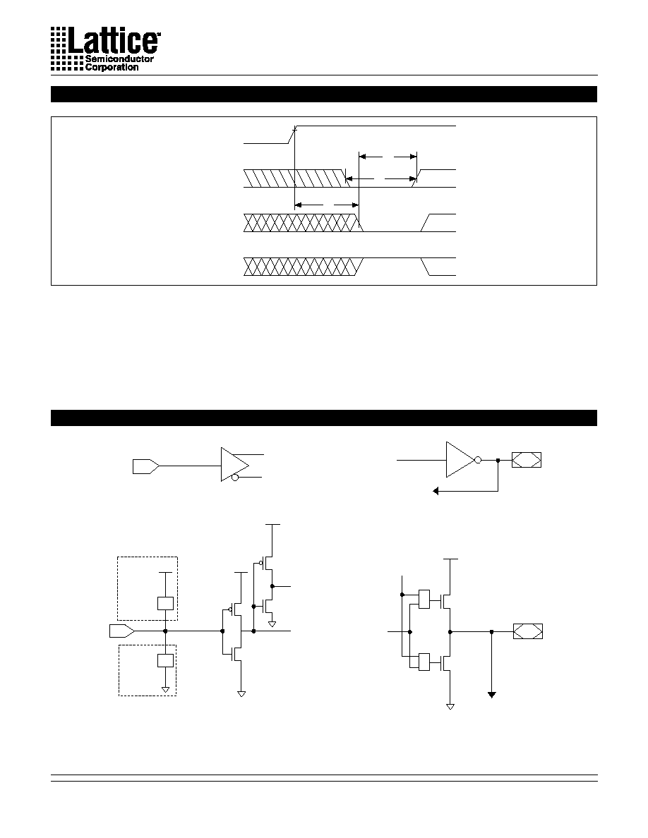
INPUT BUFFERS
Typical Input Characteristic
Input Current (
�
A)
-40
-30
-20
-10
0
10
20
30
40
0
1
2
3
4
5
Input Voltage (Volts)
Output Register Preload
When testing state machine designs, all possible states and state
transitions must be verified in the design, not just those required
in the normal machine operations. This is because, in system
operation, certain events occur that may throw the logic into an
illegal state (power-up, line voltage glitches, brown-outs, etc.). To
test a design for proper treatment of these conditions, a way must
be provided to break the feedback paths, and force any desired
(i.e., illegal) state into the registers. Then the machine can be
sequenced and the outputs tested for correct next state condi-
tions.
The GAL16V8Z/ZD devices includes circuitry that allows each reg-
istered output to be synchronously set either high or low. Thus,
any present state condition can be forced for test sequencing. If
necessary, approved GAL programmers capable of executing test
vectors perform output register preload automatically.
Input Buffers
GAL16V8Z/ZD devices are designed with TTL level compatible
input buffers. These buffers, with their characteristically high im-
pedance, load driving logic much less than traditional bipolar de-
vices. This allows for a greater fan out from the driving logic.
GAL16V8Z/ZD input buffers have latches within the buffers. As
a result, when the device goes into standby mode the inputs will
be latched to its values prior to standby. In order to overcome the
input latches, they will have to be driven by an external source.
Lattice Semiconductor recommends that all unused inputs and
tri-stated I/O pins for both devices be connected to another ac-
tive input, V
CC
, or GND. Doing this will tend to improve noise im-
munity and reduce I
CC
for the device.
Specifications
GAL16V8Z
GAL16V8ZD
17
Vcc
CLK
INTERNAL REGISTER
Q - OUTPUT
FEEDBACK/EXTERNAL
OUTPUT REGISTER
Vcc (min.)
t
pr
Internal Register
Reset to Logic "0"
Device Pin
Reset to Logic "1"
t
wl
t
su
asynchronous nature of system power-up, some conditions must
be met to provide a valid power-up reset of the GAL16V8Z/ZD.
First, the V
CC
rise must be monotonic. Second, the clock input
must be at static TTL level as shown in the diagram during power
up. The registers will reset within a maximum of
t
pr time. As in
normal system operation, avoid clocking the device until all in-
put and feedback path setup times have been met. The clock
must also meet the minimum pulse width requirements.
Vcc
PIN
Vcc
ESD
Protection
Circuit
ESD
Protection
Circuit
Vcc
PIN
Vcc
PIN
Tri-State
Control
Feedback
(To Input Buffer)
PIN
Feedback
Data
Output
Typical Input
Typical Output
Circuitry within the GAL16V8Z/ZD provides a reset signal to all
registers during power-up. All internal registers will have their
Q outputs set low after a specified time (
t
pr, 1
�
s MAX). As a result,
the state on the registered output pins (if they are enabled) will
always be high on power-up, regardless of the programmed
polarity of the output pins. This feature can greatly simplify state
machine design by providing a known state on power-up. The
timing diagram for power-up is shown below. Because of the
Power-Up Reset
Input/Output Equivalent Schematics
Specifications
GAL16V8Z
GAL16V8ZD
18
Normalized Tpd vs Vcc
Supply Voltage (V)
Normalized Tpd
0.8
0.9
1
1.1
1.2
4.50
4.75
5.00
5.25
5.50
PT H->L
PT L->H
Normalized Tco vs Vcc
Supply Voltage (V)
Normalized Tco
0.8
0.9
1
1.1
1.2
4.50
4.75
5.00
5.25
5.50
RISE
FALL
Normalized Tsu vs Vcc
Supply Voltage (V)
Normalized Tsu
0.8
0.9
1
1.1
1.2
1.3
1.4
4.50
4.75
5.00
5.25
5.50
PT H->L
PT L->H
Normalized Tpd vs Temp
Temperature (deg. C)
Normalized Tpd
0.7
0.8
0.9
1
1.1
1.2
1.3
-55
-25
0
25
50
75
100
125
PT H->L
PT L->H
Normalized Tco vs Temp
Temperature (deg. C)
Normalized Tco
0.7
0.8
0.9
1
1.1
1.2
1.3
-55
-25
0
25
50
75
100
125
RISE
FALL
Normalized Tsu vs Temp
Temperature (deg. C)
Normalized Tsu
0.7
0.8
0.9
1
1.1
1.2
1.3
1.4
-55
-25
0
25
50
75
100
125
PT H->L
PT L->H
Delta Tpd vs # of Outputs
Switching
Number of Outputs Switching
Delta Tpd (ns)
-2
-1.5
-1
-0.5
0
1
2
3
4
5
6
7
8
RISE
FALL
Delta Tco vs # of Outputs
Switching
Number of Outputs Switching
Delta Tco (ns)
-2
-1.5
-1
-0.5
0
1
2
3
4
5
6
7
8
RISE
FALL
Delta Tpd vs Output Loading
Output Loading (pF)
Delta Tpd (ns)
-2
0
2
4
6
8
10
0
50
100
150
200
250
300
RISE
FALL
Delta Tco vs Output Loading
Output Loading (pF)
Delta Tco (ns)
-2
0
2
4
6
8
10
0
50
100
150
200
250
300
RISE
FALL
Typical AC and DC Characteristics
Specifications
GAL16V8Z
GAL16V8ZD
19
Vol vs Iol
Iol (mA)
Vol (V)
0
0.25
0.5
0.75
1
1.25
1.5
0.00
20.00
40.00
60.00
Voh vs Ioh
Ioh(mA)
Voh (V)
0
1
2
3
4
5
0.00
10.00
20.00
30.00
40.00
50.00
60.00
Voh vs Ioh
Ioh(mA)
Voh (V)
2.5
3
3.5
4
4.5
5
0.00
1.00
2.00
3.00
4.00
Normalized Icc vs Vcc
Supply Voltage (V)
Normalized Icc
0.70
0.80
0.90
1.00
1.10
1.20
1.30
4.50
4.75
5.00
5.25
5.50
Normalized Icc vs Temp
Temperature (deg. C)
Normalized Icc
0.8
0.9
1
1.1
1.2
-55
-25
0
25
50
75
100
125
Normalized Icc vs Freq. (DPP
& ITD > 10MHz)
Frequency (MHz)
Normalized Icc
0.80
0.90
1.00
1.10
1.20
1.30
0
25
50
75
100
Delta Icc vs Vin (1 input)
Vin (V)
Delta Icc (mA)
0
1
2
3
4
5
0.00 0.50 1.00 1.50 2.00 2.50 3.00 3.50 4.00
Input Clamp (Vik)
Vik (V)
Iik (mA)
0
10
20
30
40
50
60
70
80
90
-1.00
-0.80
-0.60
-0.40
-0.20
0.00
Normalized Icc vs Freq. (ITD)
Frequency (KHz)
Normalized Icc
0
0.2
0.4
0.6
0.8
1
1
10
100
1000
10000
Typical AC and DC Characteristics