
GAL20RA10
High-Speed Asynchronous E
2
CMOS PLD
Generic Array LogicTM
1
1
12
13
24
PL
I
I
I
I
I
I
I
I
I
I
GND
Vcc
I/O/Q
I/O/Q
I/O/Q
I/O/Q
I/O/Q
I/O/Q
I/O/Q
I/O/Q
I/O/Q
I/O/Q
OE
6
18
DIP
PLCC
2
28
NC
PL
I
I
I
I
I
I
I
I
NC
NC
NC
GND
I
I
OE
I/O/Q
I/O/Q
I/O/Q
I/O/Q
I/O/Q
I/O/Q
I/O/Q
Vcc
I/O/Q
I/O/Q
I/O/Q
4
7
5
9
11
12
14
16
18
19
21
23
25
26
GAL
20RA10
Features
� HIGH PERFORMANCE E
2
CMOS
�
TECHNOLOGY
-- 7.5 ns Maximum Propagation Delay
-- Fmax = 83.3 MHz
-- 9 ns Maximum from Clock Input to Data Output
-- TTL Compatible 8 mA Outputs
-- UltraMOS
�
Advanced CMOS Technology
� 50% to 75% REDUCTION IN POWER FROM BIPOLAR
-- 75mA Typical Icc
� ACTIVE PULL-UPS ON ALL PINS
� E
2
CELL TECHNOLOGY
-- Reconfigurable Logic
-- Reprogrammable Cells
-- 100% Tested/100% Yields
-- High Speed Electrical Erasure (<100 ms)
-- 20 Year Data Retention
� TEN OUTPUT LOGIC MACROCELLS
-- Independent Programmable Clocks
-- Independent Asynchronous Reset and Preset
-- Registered or Combinatorial with Polarity
-- Full Function and Parametric Compatibility with
PAL20RA10
� PRELOAD AND POWER-ON RESET OF ALL REGISTERS
-- 100% Functional Testability
� APPLICATIONS INCLUDE:
-- State Machine Control
-- Standard Logic Consolidation
-- Multiple Clock Logic Designs
� ELECTRONIC SIGNATURE FOR IDENTIFICATION
GAL20RA10
Top View
PROGRAMMABLE
AND-ARRAY
(80X40)
OE
PL
I
I/O/Q
8
OLMC
I/O/Q
8
OLMC
I/O/Q
8
OLMC
I/O/Q
8
OLMC
I/O/Q
8
OLMC
I/O/Q
8
OLMC
I/O/Q
8
OLMC
I/O/Q
8
OLMC
I/O/Q
8
OLMC
I/O/Q
8
OLMC
I
I
I
I
I
I
I
I
I
Copyright � 1997 Lattice Semiconductor Corp. All brand or product names are trademarks or registered trademarks of their respective holders. The specifications and information herein are subject
to change without notice.
LATTICE SEMICONDUCTOR CORP., 5555 Northeast Moore Ct., Hillsboro, Oregon 97124, U.S.A.
July 1997
Tel. (503) 681-0118; 1-888-ISP-PLDS; FAX (503) 681-3037; http://www.latticesemi.com
20ra10_02
Description
The GAL20RA10 combines a high performance CMOS process
with electrically erasable (E
2
) floating gate technology to provide
the highest speed performance available in the PLD market. Lattice
Semiconductor's E
2
CMOS circuitry achieves power levels as low
as 75mA typical I
CC
which represents a substantial savings in power
when compared to bipolar counterparts. E
2
technology offers high
speed (<100ms) erase times providing the ability to reprogram,
reconfigure or test the devices quickly and efficiently.
The generic architecture provides maximum design flexibility by
allowing the Output Logic Macrocell (OLMC) to be configured by
the user. The GAL20RA10 is a direct parametric compatible CMOS
replacement for the PAL20RA10 device.
Unique test circuitry and reprogrammable cells allow complete AC,
DC, and functional testing during manufacturing. Therefore, Lattice
Semiconductor delivers 100% field programmability and function-
ality of all GAL products. In addition, 100 erase/write cycles and
data retention in excess of 20 years are specified.
Functional Block Diagram
Pin Configuration

Specifications
GAL20RA10
2
)
s
n
(
d
p
T
)
s
n
(
u
s
T
)
s
n
(
o
c
T
)
A
m
(
c
c
I
#
g
n
i
r
e
d
r
O
e
g
a
k
c
a
P
5
.
7
3
9
0
0
1
J
L
7
-
B
0
1
A
R
0
2
L
A
G
C
C
L
P
d
a
e
L
-
8
2
0
1
4
1
1
0
0
1
P
L
0
1
-
B
0
1
A
R
0
2
L
A
G
P
I
D
c
i
t
s
a
l
P
n
i
P
-
4
2
0
0
1
J
L
0
1
-
B
0
1
A
R
0
2
L
A
G
C
C
L
P
d
a
e
L
-
8
2
5
1
7
5
1
0
0
1
P
L
5
1
-
B
0
1
A
R
0
2
L
A
G
P
I
D
c
i
t
s
a
l
P
n
i
P
-
4
2
0
0
1
J
L
5
1
-
B
0
1
A
R
0
2
L
A
G
C
C
L
P
d
a
e
L
-
8
2
0
2
0
1
0
2
0
0
1
P
L
0
2
-
B
0
1
A
R
0
2
L
A
G
P
I
D
c
i
t
s
a
l
P
n
i
P
-
4
2
0
0
1
J
L
0
2
-
B
0
1
A
R
0
2
L
A
G
C
C
L
P
d
a
e
L
-
8
2
0
3
0
2
0
3
0
0
1
P
L
0
3
-
B
0
1
A
R
0
2
L
A
G
P
I
D
c
i
t
s
a
l
P
n
i
P
-
4
2
0
0
1
J
L
0
3
-
B
0
1
A
R
0
2
L
A
G
C
C
L
P
d
a
e
L
-
8
2
Industrial Grade Specifications
)
s
n
(
d
p
T
)
s
n
(
u
s
T
)
s
n
(
o
c
T
)
A
m
(
c
c
I
#
g
n
i
r
e
d
r
O
e
g
a
k
c
a
P
0
2
0
1
0
2
0
2
1
I
P
L
0
2
-
B
0
1
A
R
0
2
L
A
G
P
I
D
c
i
t
s
a
l
P
n
i
P
-
4
2
0
2
1
I
J
L
0
2
-
B
0
1
A
R
0
2
L
A
G
C
C
L
P
d
a
e
L
-
8
2
Blank = Commercial
I = Industrial
Grade
Package
Power
L = Low Power
Speed (ns)
XXXXXXXX
XX
X
X X
Device Name
_
P = Plastic DIP
J = PLCC
GAL20RA10B
GAL20RA10 Ordering Information
Commercial Grade Specifications
Part Number Description

Specifications
GAL20RA10
3
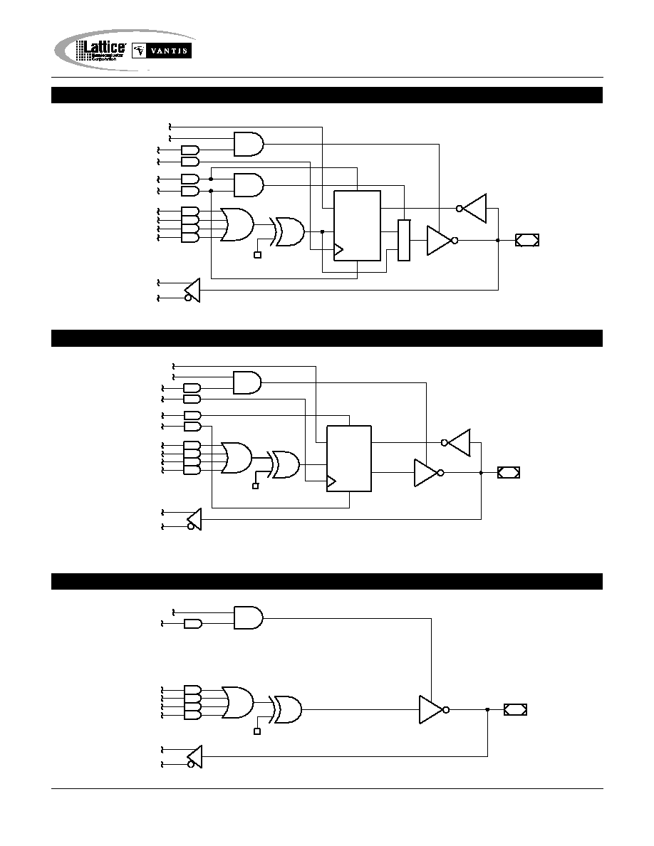
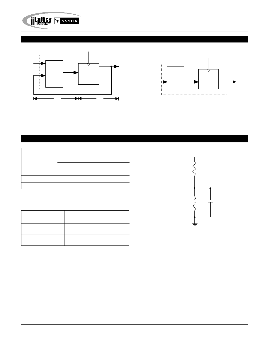
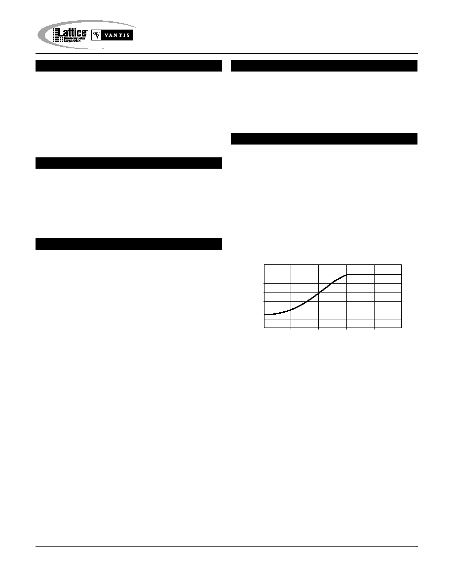
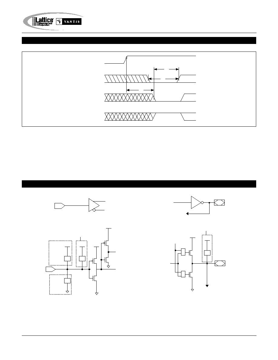
Output Logic Macrocell (OLMC)
The GAL20RA10 OLMC consists of 10 D flip-flops with indi-
vidual asynchronous programmable reset, preset and clock product
terms. The sum of four product terms and an Exclusive-OR pro-
vide a programmable polarity D-input to each flip-flop. An output
enable term combined with the dedicated output enable pin pro-
vides tri-state control of each output. Each OLMC has a flip-flop
bypass, allowing any combination of registered or combinatorial
outputs.
The GAL20RA10 has 10 dedicated input pins and 10 program-
mable I/O pins, which can be either inputs, outputs, or dynamic I/
O. Each pin has a unique path to the logic array. All macrocells
have the same type and number of data and control product terms,
allowing the user to exchange I/O pin assignments without restric-
tion.
Independent Programmable Clocks
An independent clock control product term is provided for each
GAL20RA10 macrocell. Data is clocked into the flip-flop on the
active edge of the clock product term. The use of individual clock
control product terms allow up to ten separate clocks. These clocks
can be derived from any pin or combination of pins and/or feedback
from other flip-flops. Multiple clock sources allow a number of
asynchronous register functions to be combined into a single
GAL20RA10. This allows the designer to combine discrete logic
functions into a single device.
Programmable Polarity
The polarity of the D-input to each macrocell flip-flop is individually
programmable to be active high or low. This is accomplished with
a programmable Exclusive-OR gate on the D-input of each flip-
flop. The polarity of the pin is active low when XOR bit is pro-
grammed (or zero) and is active high when XOR bit is erased (or
one). Because of the inverted output buffer, the XOR gate output
node is opposite polarity from the pin. It should be noted that the
programmable polarity only affects the data latched into the flip-flop
on the active edge of the clock product term. The reset, preset and
preload will alter the state of the flip-flop independent of the state
of programmable polarity bit. The ability to program the active po-
larity of the D-inputs can be used to reduce the total number of
product terms used, by allowing the DeMorganization of the logic
functions. This logic reduction is accomplished by the logic com-
piler, and does not require the designer to define the polarity.
Output Enable
The output of each GAL20RA10 macrocell is controlled by the
"AND'ing" of an independent output enable product term and a
common active low output enable pin (pin 13 on DIP package / pin
16 on PLCC package). The output is enabled while the output en-
able product term is active and the output enable pin is low. This
output control structure allows several output enable alternatives.
Combinatorial Control
The register in each GAL20RA10 macrocell may be bypassed by
asserting both the reset and preset product terms. While both
product terms are active the flip-flop is bypassed and the D- input
is presented directly to the inverting output buffer. This provides
the designer the ability to dynamically configure any macrocell as
a combinatorial output, or to fix the macrocell as combinatorial only
by forcing both reset and preset product terms active. Some logic
compilers will configure macrocells as registered or combinatorial
based on the logic equations, others require the designer to force
the reset and preset product terms active for combinatorial
macrocells.
Parallel Flip-Flop Preload
The flip-flops of a GAL20RA10 can be reset or preset from the
I/O pins by applying a logic low to the preload pin (pin 1 on DIP
package / pin 2 on PLCC package) and applying the desired logic
level to each I/O pin. The I/O pins must remain valid for the preload
setup and hold time. All 10 flip-flops are reset or preset during
preload, independent of all other OLMC inputs.
A logic low on an I/O pin during preload will preset the flip-flop, a
logic high will reset the flip-flop. The output of any flip-flop to be
preloaded must be disabled. Enabling the output during preload
will maintain the current logic state. It should be noted that the
preload alters the state of the flip-flop whose output is inverted by
the output buffer. A reset of the flip-flop will result in the output pin
becoming a logic high and a preset will result in a logic low. Note
that the common output enable pin will disable all 10 outputs of the
GAL20RA10 when held high.
RESET PRESET FUNCTION
0
0
Registered function of data product term
1
0
Reset register to "0" (device pin = "1")
0
1
Preset register to "1" (device pin = "0")
1
1
Register-bypass (combinatorial output)
Asynchronous Reset and Preset
Each GAL20RA10 macrocell has an independent asynchronous
reset and preset control product term. The reset and preset product
terms are level sensitive, and will hold the flip-flop in the reset or
preset state while the product term is active independent of the clock
or D-inputs. It should be noted that the reset and preset term al-
ter the state of the flip-flop whose output is inverted by the output
buffer. A reset of the flip-flop will result in the output pin becoming
a logic high and a preset will result in a logic low.
Specifications
GAL20RA10
4
PD
AP
AR
PL
D
Q
XOR (n)
PL
OE
0
1
PD
AP
AR
PL
D
Q
XOR (n)
PL
OE
XOR (n)
OE
Output Logic Macrocell Diagram
Output Logic Macrocell Configuration (Registered With Polarity)
Output Logic Macrocell Configuration (Combinatorial With Polarity)

Specifications
GAL20RA10
5
DIP (PLCC) Package Pinouts
36
32
28
24
20
16
12
8
4
0
OLMC
XOR - 3209
XOR - 3208
OLMC
XOR - 3207
OLMC
OLMC
XOR - 3206
OLMC
XOR - 3205
OLMC
OLMC
XOR - 3204
XOR - 3203
OLMC
XOR - 3202
OLMC
XOR - 3200
XOR - 3201
OLMC
0
280
320
600
640
920
960
1240
1280
1560
1600
1880
1920
2200
2240
2520
2560
2840
2880
3160
OE
PL
1 (2)
2 (3)
3 (4)
4 (5)
5 (6)
6 (7)
7 (9)
8 (10)
9 (11)
13 (16)
14 (17)
15 (18)
16 (19)
17 (20)
19 (23)
20 (24)
23 (27)
10 (12)
11 (13)
18 (21)
22 (26)
21 (25)
64-USER ELECTRONIC SIGNATURE FUSES
3210, 3211, .... .... 3272, 3273
Byte7 Byte6 .... .... Byte1 Byte0
MSB LSB
GAL20RA10 Logic Diagram

Specifications
GAL20RA10B
6
Recommended Operating Conditions
Commercial Devices:
Ambient Temperature (T
A
) ............................. 0 to +75
�
C
Supply voltage (V
CC
)
with Respect to Ground ..................... +4.75 to +5.25V
Industrial Devices:
Ambient Temperature (T
A
) ..........................-40 to +85
�
C
Supply voltage (V
CC
)
with Respect to Ground ..................... +4.50 to +5.50V
Absolute Maximum Ratings
(1)
Supply voltage V
CC
....................................... -0.5 to +7V
Input voltage applied ........................... -2.5 to V
CC
+1.0V
Off-state output voltage applied .......... -2.5 to V
CC
+1.0V
Storage Temperature ................................. -65 to 150
�
C
Ambient Temperature with
Power Applied ......................................... -55 to 125
�
C
1.Stresses above those listed under the "Absolute Maximum
Ratings" may cause permanent damage to the device. These
are stress only ratings and functional operation of the device at
these or at any other conditions above those indicated in the
operational sections of this specification is not implied (while
programming, follow the programming specifications).
DC Electrical Characteristics
Over Recommended Operating Conditions (Unless Otherwise Specified)
V
IL
Input Low Voltage
Vss � 0.5
--
0.8
V
V
IH
Input High Voltage
2.0
--
Vcc+1
V
I
IL
1
Input or I/O Low Leakage Current
0V
V
IN
V
IL
(MAX.)
--
--
-100
�
A
I
IH
Input or I/O High Leakage Current
3.5V
V
IN
V
CC
--
--
10
�
A
V
OL
Output Low Voltage
I
OL
= MAX. Vin = V
IL
or V
IH
--
--
0.5
V
V
OH
Output High Voltage
I
OH
= MAX. Vin = V
IL
or V
IH
2.4
--
--
V
I
OL
Low Level Output Current
--
--
8
mA
I
OH
High Level Output Current
--
--
-3.2
mA
I
OS
2
Output Short Circuit Current
V
CC
= 5V
V
OUT
= 0.5V T
A
= 25
�
C
-50
--
-135
mA
COMMERCIAL
I
CC
Operating Power
V
IL
= 0.5V V
IH
= 3.0V
L -7/-10/-15/-20/-30
--
75
100
mA
Supply Current
f
toggle
= 15MHz Outputs Open
SYMBOL
PARAMETER
CONDITION
MIN.
TYP.
3
MAX.
UNITS
INDUSTRIAL
I
CC
Operating Power
V
IL
= 0.5V V
IH
= 3.0V
L -20
--
75
120
mA
Supply Current
f
toggle
= 15MHz Outputs Open
1) The leakage current is due to the internal pull-up resistor on all pins. See Input Buffer section for more information.
2) One output at a time for a maximum duration of one second. Vout = 0.5V was selected to avoid test problems caused by tester
ground degradation. Characterized but not 100% tested.
3) Typical values are at Vcc = 5V and T
A
= 25
�
C

Specifications
GAL20RA10B
7
SYMBOL
PARAMETER
MAXIMUM*
UNITS
TEST CONDITIONS
C
I
Input Capacitance
8
pF
V
CC
= 5.0V, V
I
= 2.0V
C
I/O
I/O Capacitance
10
pF
V
CC
= 5.0V, V
I/O
= 2.0V
*Characterized but not 100% tested.
t
pd
A
Input or I/O to Combinatorial Output
2
7.5
2
10
--
15
--
20
--
30
ns
t
co
A
Clock to Output Delay
2
9
2
11
--
15
--
20
--
30
ns
t
su
--
Setup Time, Input or Fdbk before Clk
3
--
4
--
7
--
10
--
20
--
ns
t
h
--
Hold Time, Input or Fdbk after Clk
2
--
3
--
3
--
3
--
10
--
ns
f
max
3
A
Maximum Clock Frequency with
83.3
--
66.7
--
45.0
--
33.3
--
20.0
--
MHz
External Feedback, 1/(tsu + tco)
A
Maximum Clock Frequency with
83.3
--
71.4
--
50.0
--
41.7
--
25.0
--
MHz
No Feedback
t
wh
--
Clock Pulse Duration, High
6
--
7
--
10
--
12
--
20
--
ns
t
wl
--
Clock Pulse Duration, Low
6
--
7
--
10
--
12
--
20
--
ns
t
en/
t
dis
B,C
I or I/O to Output Enabled / Disabled
--
7.5
--
10
--
15
--
20
--
30
ns
t
en/
t
dis
B,C
OE
to Output Enabled / Disabled
--
5
--
9
--
12
--
15
--
20
ns
t
ar/
t
ap
A
Input or I/O to Async. Reset / Preset
--
9
--
11
--
15
--
20
--
30
ns
t
arw/
t
apw
--
Async. Reset / Preset Pulse Duration
6
--
10
--
15
--
20
--
20
--
ns
t
arr/
t
apr
--
Async. Reset / Preset Recovery Time
7
--
7
--
10
--
12
--
20
--
ns
t
wp
--
Preload Pulse Duration
8
--
10
--
15
--
20
--
30
--
ns
t
sp
--
Preload Setup Time
5
--
7
--
10
--
15
--
25
--
ns
t
hp
--
Preload Hold Time
5
--
7
--
10
--
15
--
25
--
ns
UNITS
-30
MIN.
MAX.
-20
MIN.
MAX.
-15
MIN.
MAX.
-10
MIN.
MAX.
PARAM.
DESCRIPTION
TEST
COND
1
.
-7
MIN.
MAX.
COM
COM
COM
COM / IND
COM
1) Refer to Switching Test Conditions section.
2) Refer to fmax Descriptions section.
AC Switching Characteristics
Over Recommended Operating Conditions
Capacitance (T
A
= 25
�
C, f = 1.0 MHz)

Specifications
GAL20RA10
8
Combinatorial Output
Registered Output
Clock Width
Input or I/O to Output Enable/Disable
t
wp
t
sp
t
hp
PL
ALL I/O
PINS
Parallel Preload
INPUT or
I/O FEEDBACK
DRIVING AP or AR
CLK
VALID INPUT
t
apr/arr
t
apw/arw
Asynchronous Reset and Preset Recovery
Asynchronous Reset and Preset
OE
OE
OE
OE
OE
to Enable / Disable
INPUT or
I/O FEEDBACK
REGISTERED
OUTPUT
CLK
VALID INPUT
t
su
t
co
t
h
VALID CLOCK
VALID CLOCK
OE
t
en
t
dis
OUTPUT
CLK
t
wh
t
wl
VALID INPUT
INPUT or
I/O FEEDBACK
t
pd
COMBINATORIAL
OUTPUT
t
en
t
dis
INPUT or
I/O FEEDBACK
OUTPUT
VALID INPUT
t
ar
t
ap
INPUT or
I/O FEEDBACK
Q-OUTPUT OF
REGISTER
REGISTERED
OUTPUT PIN
Q-OUTPUT OF
REGISTER
REGISTERED
OUTPUT PIN
Switching Waveforms
Specifications
GAL20RA10
9
Note: fmax with external feedback is cal-
culated from measured tsu and tco.
f
max with External Feedback 1/(
t
su+
t
co)
Input Pulse Levels
GND to 3.0V
Input Rise and
-7/-10
2ns 10% � 90%
Fall Times
-15/-20/-30
3ns 10% � 90%
Input Timing Reference Levels
1.5V
Output Timing Reference Levels
1.5V
Output Load
See Figure
3-state levels are measured 0.5V from steady-state active
level.
Output Load Conditions (see figure)
Test Condition
R
1
R
2
C
L
A
470
390
50pF
B
Active High
390
50pF
Active Low
470
390
50pF
C
Active High
390
5pF
Active Low
470
390
5pF
TEST POINT
C *
L
FROM OUTPUT (O/Q)
UNDER TEST
+5V
*C
L
INCLUDES TEST FIXTURE AND PROBE CAPACITANCE
R
2
R
1
REGISTER
LOGIC
ARRAY
t
co
t
su
CLK
f
max with No Feedback
Note: fmax with no feedback may be less
than 1/(twh + twl). This is to allow for a
clock duty cycle of other than 50%.
REGISTER
LOGIC
ARRAY
CLK
f
max Descriptions
Switching Test Conditions
Specifications
GAL20RA10
10
Typical Input Pull-up Characteristic
Electronic Signature
An electronic signature word is provided in every GAL20RA10
device. It contains 64 bits of reprogrammable memory that con-
tains user defined data. Some uses include user ID codes, revi-
sion numbers, pattern identification or inventory control codes. The
signature data is always available to the user independent of the
state of the security cell.
NOTE: The electronic signature bits if programmed to any value
other then zero(0) will alter the checksum of the device.
Security Cell
A security cell is provided in every GAL20RA10 device as a deter-
rent to unauthorized copying of the device pattern. Once pro-
grammed, this cell prevents further read access of the device
pattern information. This cell can be only be reset by reprogram-
ming the device. The original pattern can never be examined once
this cell is programmed. The Electronic Signature is always avail-
able regardless of the security cell state.
Latch-Up Protection
GAL20RA10 devices are designed with an on-board charge pump
to negatively bias the substrate. The negative bias is of sufficient
magnitude to prevent input undershoots from causing the circuitry
to latch. Additionally, outputs are designed with n-channel pullups
instead of the traditional p-channel pullups to eliminate any pos-
sibility of SCR induced latching.
1 . 0
2 . 0
3 . 0
4 . 0
5 . 0
- 6 0
0
- 2 0
- 4 0
0
In p u t V o lt ag e ( V o lt s)
I
nput
C
u
r
r
e
nt
(
u
A
)
Device Programming
GAL devices are programmed using a Lattice Semiconductor-
approved Logic Programmer, available from a number of manu-
facturers (see the the GAL Development Tools section). Complete
programming of the device takes only a few seconds. Erasing of
the device is transparent to the user, and is done automatically as
part of the programming cycle.
Input Buffers
GAL20RA10 devices are designed with TTL level compatible in-
put buffers. These buffers have a characteristically high impedance
and present a much lighter load to the driving logic than traditional
bipolar devices.
GAL20RA10 input buffers have active pull-ups within their input
structure. As a result, unused inputs and I/Os will float to a TTL
"high" (logical "1"). Lattice Semiconductor recommends that all un-
used inputs and tri-stated I/O pins be connected to another active
input, Vcc, or GND. Doing this will tend to improve noise immu-
nity and reduce Icc for the device.
Specifications
GAL20RA10
11
Vcc
PIN
Vcc
Vref
Active Pull-up
Circuit
ESD
Protection
Circuit
ESD
Protection
Circuit
Vcc
PIN
Typical Input
Circuitry within the GAL20RA10 provides a reset signal to all reg-
isters during power-up. All internal registers will have their Q
outputs set low after a specified time (tpr, 1
�
s MAX). As a result,
the state on the registered output pins (if they are enabled) will
be high on power-up, because of the inverting buffer on the output
pins. This feature can greatly simplify state machine design by
providing a known state on power-up. The timing diagram for
power-up is shown to the right. Because of the asynchronous
Vcc
CLK
INTERNAL REGISTER
Q - OUTPUT
FEEDBACK/EXTERNAL
OUTPUT REGISTER
Vcc (min.)
t
pr
Internal Register
Reset to Logic "0"
Device Pin
Reset to Logic "1"
t
wl
t
su
nature of system power-up, some conditions must be met to
provide a valid power-up reset of the GAL20RA10. First, the Vcc
rise must be monotonic. Second, the clock input must be at a static
TTL level as shown in the diagram during power up. The regis-
ters will reset within a maximum of 1
�
s. As in normal system op-
eration, avoid clocking the device until all input and feedback path
setup times have been met. The clock must also meet the mini-
mum pulse width requirements.
(Vref Typical = 3.2V)
(Vref Typical = 3.2V)
Vcc
PIN
Vref
Tri-State
Control
Active Pull-up
Circuit
Feedback
(To Input Buffer)
PIN
Feedback
Data
Output
Typical Output
Power-Up Reset
Input/Output Equivalent Schematics
Specifications
GAL20RA10
12
Normalized Tpd vs Vcc
Supply Voltage (V)
Normalized Tpd
0.8
0.9
1
1.1
1.2
4.50
4.75
5.00
5.25
5.50
Normalized Tco vs Vcc
Supply Voltage (V)
Normalized Tco
0.8
0.9
1
1.1
1.2
4.50
4.75
5.00
5.25
5.50
Normalized Tsu vs Vcc
Supply Voltage (V)
Normalized Tsu
0.6
0.8
1
1.2
1.4
4.50
4.75
5.00
5.25
5.50
Normalized Tpd vs Temp
Temperature (deg. C)
Normalized Tpd
0.7
0.8
0.9
1
1.1
1.2
1.3
-55
-25
0
25
50
75
100
125
Normalized Tco vs Temp
Temperature (deg. C)
Normalized Tco
0.7
0.8
0.9
1
1.1
1.2
1.3
-55
-25
0
25
50
75
100
125
Normalized Tsu vs Temp
Temperature (deg. C)
Normalized Tsu
0.6
0.8
1
1.2
1.4
1.6
-55
-25
0
25
50
75
100
125
Delta Tpd vs # of Outputs
Switching
Number of Outputs Switching
Delta Tpd (ns)
-1.5
-1
-0.5
0
1
2
3
4
5
6
7
8
9
10
Delta Tco vs # of Outputs
Switching
Number of Outputs Switching
Delta Tco (ns)
-2
-1.5
-1
-0.5
0
1
2
3
4
5
6
7
8
9
10
Delta Tpd vs Output
Loading
Output Loading (pF)
Delta Tpd (ns)
-4
-2
0
2
4
6
8
0
50
100
150
RISE
FALL
Delta Tco vs Output
Loading
Output Loading (pF)
Delta Tco (ns)
-4
-2
0
2
4
6
8
0
50
100
150
RISE
FALL
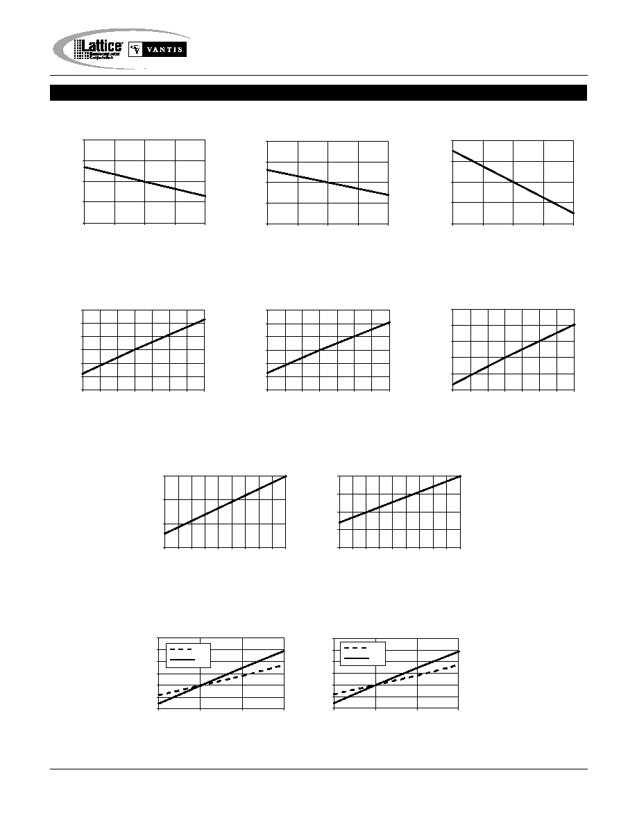
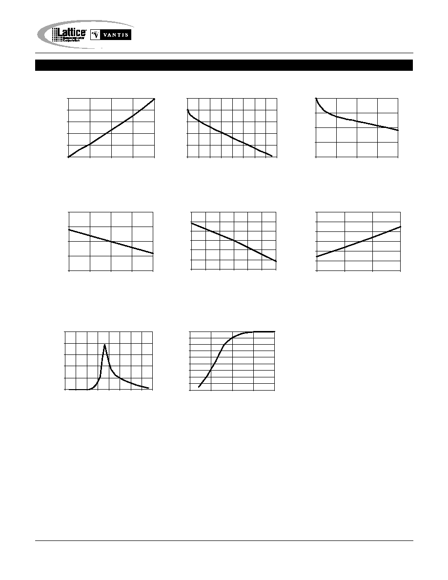
GAL10RA10B-7/-10: Typical AC and DC Characteristic Diagrams
Specifications
GAL20RA10
13
Vol vs Iol
Iol (mA)
Vol (V)
0
0.2
0.4
0.6
0.8
1
0
10
20
30
40
Voh vs Ioh
Ioh(mA)
Voh (V)
0
1
2
3
4
5
0
10
20
30
40
50
60
70
80
Voh vs Ioh
Ioh(mA)
Voh (V)
3
3.25
3.5
3.75
4
0.00
1.00
2.00
3.00
4.00
Normalized Icc vs Vcc
Supply Voltage (V)
Normalized Icc
0.8
0.9
1
1.1
1.2
4.50
4.75
5.00
5.25
5.50
Normalized Icc vs Temp
Temperature (deg. C)
Normalized Icc
0.7
0.8
0.9
1
1.1
1.2
1.3
-55
-25
0
25
75
100
125
Normalized Icc vs Freq.
Frequency (MHz)
Normalized Icc
0.80
0.90
1.00
1.10
1.20
1.30
1.40
0
25
50
75
Delta Icc vs Vin (1 input)
Vin (V)
Delta Icc (mA)
0
2
4
6
8
10
0.20 0.70 1.20 1.70 2.20 2.70 3.20 3.70
Input Clamp (Vik)
Vik (V)
Iik (mA)
0
10
20
30
40
50
60
70
80
90
-2.00
-1.50
-1.00
-0.50
0.00
GAL10RA10B-7/-10: Typical AC and DC Characteristic Diagrams

Specifications
GAL20RA10
14
Normalized Tpd vs Vcc
Supply Voltage (V)
Normalized Tpd
0.8
0.9
1
1.1
1.2
4.50
4.75
5.00
5.25
5.50
PT H->L
PT L->H
Normalized Tco vs Vcc
Supply Voltage (V)
Normalized Tco
0.9
0.95
1
1.05
1.1
4.50
4.75
5.00
5.25
5.50
RISE
FALL
Normalized Tsu vs Vcc
Supply Voltage (V)
Normalized Tsu
0.4
0.6
0.8
1
1.2
1.4
1.6
4.50
4.75
5.00
5.25
5.50
Normalized Tpd vs Temp
Temperature (deg. C)
Normalized Tpd
0.7
0.8
0.9
1
1.1
1.2
1.3
-55
-25
0
25
50
75
90
125
PT H->L
PT L->H
Normalized Tco vs Temp
Temperature (deg. C)
Normalized Tco
0.7
0.8
0.9
1
1.1
1.2
1.3
-55
-25
0
25
50
75
90
125
RISE
FALL
Normalized Tsu vs Temp
Temperature (deg. C)
Normalized Tsu
0.6
0.7
0.8
0.9
1
1.1
1.2
1.3
1.4
-55
-25
0
25
50
75
90
125
Delta Tpd vs # of Outputs
Switching
Number of Outputs Switching
Delta Tpd (ns)
-1.2
-1
-0.8
-0.6
-0.4
-0.2
0
1
2
3
4
5
6
7
8
9
10
RISE
FALL
Delta Tco vs # of Outputs
Switching
Number of Outputs Switching
Delta Tco (ns)
-1.2
-1
-0.8
-0.6
-0.4
-0.2
0
1
2
3
4
5
6
7
8
9
10
RISE
FALL
Delta Tpd vs Output
Loading
Output Loading (pF)
Delta Tpd (ns)
-4
-2
0
2
4
6
8
10
12
0
50
100
150
200
250
300
RISE
FALL
Delta Tco vs Output
Loading
Output Loading (pF)
Delta Tco (ns)
-4
-2
0
2
4
6
8
10
12
14
0
50
100
150
200
250
300
RISE
FALL
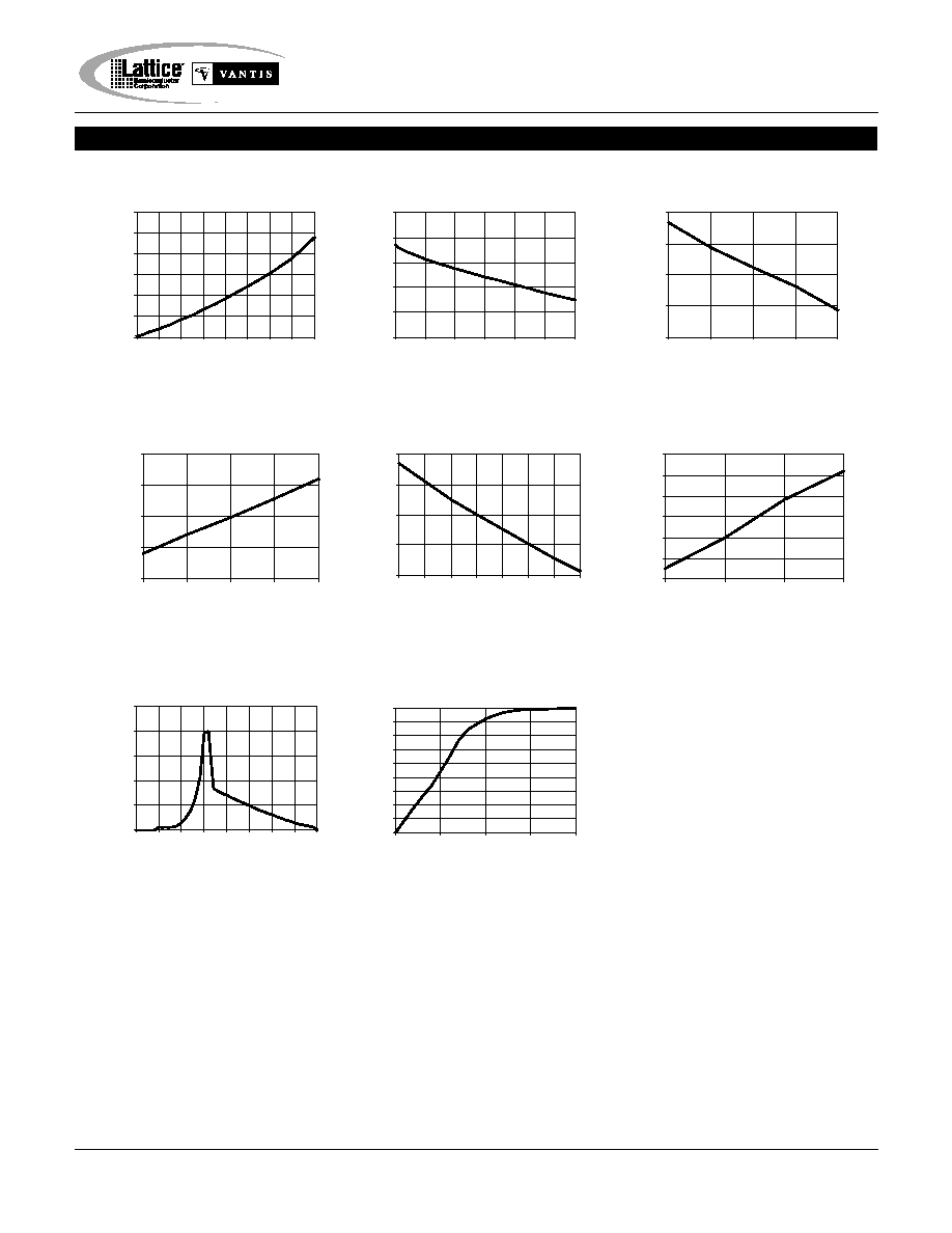
GAL10RA10B-15/-20/-30: Typical AC and DC Characteristic Diagrams
Specifications
GAL20RA10
15
Vol vs Iol
Iol (mA)
Vol (V)
0
0.5
1
1.5
2
2.5
3
0.00
20.00
40.00
60.00
80.00
Voh vs Ioh
Ioh(mA)
Voh (V)
0
1
2
3
4
5
0.00
10.00 20.00 30.00 40.00 50.00 60.00
Voh vs Ioh
Ioh(mA)
Voh (V)
3.25
3.375
3.5
3.625
3.75
0.00
1.00
2.00
3.00
4.00
Normalized Icc vs Vcc
Supply Voltage (V)
Normalized Icc
0.80
0.90
1.00
1.10
1.20
4.50
4.75
5.00
5.25
5.50
Normalized Icc vs Temp
Temperature (deg. C)
Normalized Icc
0.8
0.9
1
1.1
1.2
-55
-25
0
25
50
75
100
125
Normalized Icc vs Freq.
Frequency (MHz)
Normalized Icc
0.80
0.90
1.00
1.10
1.20
1.30
1.40
0
25
50
75
Delta Icc vs Vin (1 input)
Vin (V)
Delta Icc (mA)
0.00 0.50 1.00 1.50 2.00 2.50 3.00 3.50 4.00
Input Clamp (Vik)
Vik (V)
Iik (mA)
0
10
20
30
40
50
60
70
80
90
-2.00
-1.00
0.00
0
1
2
3
4
5
GAL10RA10B-15/-20/-30: Typical AC and DC Characteristic Diagrams