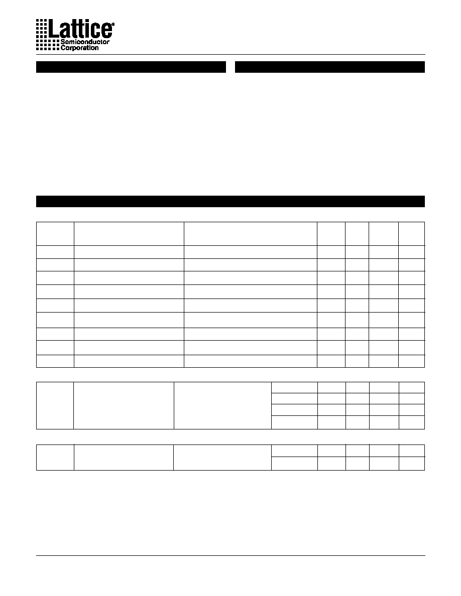
Specifications
GAL22V10
1
1
12
13
24
I
I
I
I
I
I
I
I
I
GND
I/O/Q
I/O/Q
I/O/Q
I/O/Q
I/O/Q
I/O/Q
I/O/Q
I/O/Q
I/O/Q
I/OE
6
18
I/CLK
I
Vcc
I/O/Q
2
28
NC
I/CLK
I
I
I
I
I
I
I
I
NC
NC
NC
GND
I
I
I
I/O/Q
I/O/Q
I/O/Q
I/O/Q
I/O/Q
I/O/Q
I/O/Q
Vcc
I/O/Q
I/O/Q
I/O/Q
4
26
25
19
18
21
23
16
14
12
11
9
7
5
Features
� HIGH PERFORMANCE E
2
CMOS
�
TECHNOLOGY
-- 4 ns Maximum Propagation Delay
-- Fmax = 250 MHz
-- 3.5 ns Maximum from Clock Input to Data Output
-- UltraMOS
�
Advanced CMOS Technology
� ACTIVE PULL-UPS ON ALL PINS
� COMPATIBLE WITH STANDARD 22V10 DEVICES
-- Fully Function/Fuse-Map/Parametric Compatible
with Bipolar and UVCMOS 22V10 Devices
� 50% to 75% REDUCTION IN POWER VERSUS BIPOLAR
-- 90mA Typical Icc on Low Power Device
-- 45mA Typical Icc on Quarter Power Device
� E
2
CELL TECHNOLOGY
-- Reconfigurable Logic
-- Reprogrammable Cells
-- 100% Tested/100% Yields
-- High Speed Electrical Erasure (<100ms)
-- 20 Year Data Retention
� TEN OUTPUT LOGIC MACROCELLS
-- Maximum Flexibility for Complex Logic Designs
� PRELOAD AND POWER-ON RESET OF REGISTERS
-- 100% Functional Testability
� APPLICATIONS INCLUDE:
-- DMA Control
-- State Machine Control
-- High Speed Graphics Processing
-- Standard Logic Speed Upgrade
� ELECTRONIC SIGNATURE FOR IDENTIFICATION
ESCRIPTION
Description
The GAL22V10, at 4ns maximum propagation delay time, combines
a high performance CMOS process with Electrically Erasable (E
2
)
floating gate technology to provide the highest performance avail-
able of any 22V10 device on the market. CMOS circuitry allows
the GAL22V10 to consume much less power when compared to
bipolar 22V10 devices. E
2
technology offers high speed (<100ms)
erase times, providing the ability to reprogram or reconfigure the
device quickly and efficiently.
The generic architecture provides maximum design flexibility by
allowing the Output Logic Macrocell (OLMC) to be configured by
the user. The GAL22V10 is fully function/fuse map/parametric com-
patible with standard bipolar and CMOS 22V10 devices.
Unique test circuitry and reprogrammable cells allow complete AC,
DC, and functional testing during manufacture. As a result, Lat-
tice Semiconductor delivers 100% field programmability and func-
tionality of all GAL products. In addition, 100 erase/write cycles and
data retention in excess of 20 years are specified.
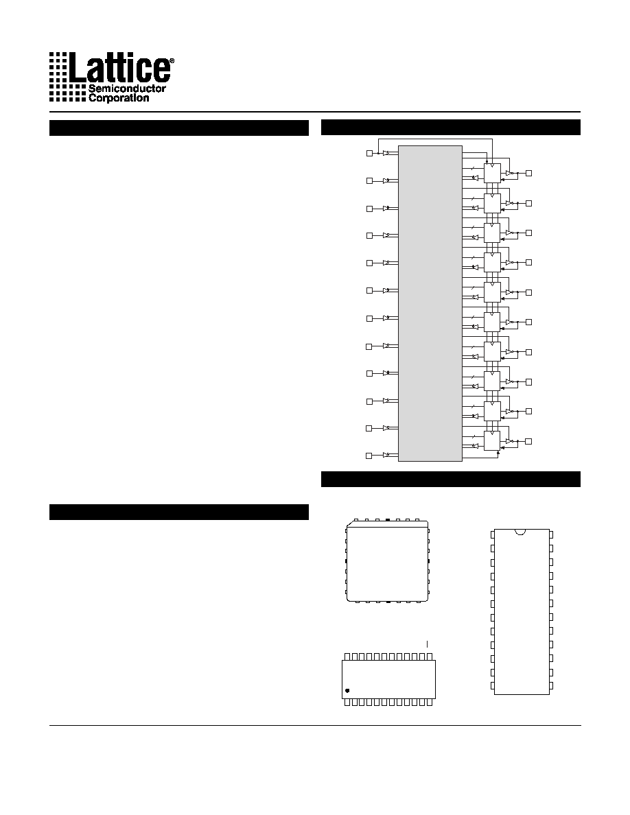
GAL22V10
High Performance E
2
CMOS PLD
Generic Array LogicTM
PROGRAMMABLE
AND-ARRAY
(132X44)
I/O/Q
I/O/Q
I/O/Q
I/O/Q
I/O/Q
I/O/Q
I/O/Q
I/O/Q
I/O/Q
I/O/Q
I
I/CLK
I
I
I
I
I
I
I
I
I
I
RESET
PRESET
8
10
12
14
16
16
14
12
10
8
OLMC
OLMC
OLMC
OLMC
OLMC
OLMC
OLMC
OLMC
OLMC
OLMC
Copyright � 2002 Lattice Semiconductor Corp. All brand or product names are trademarks or registered trademarks of their respective holders. The specifications and information herein are subject
to change without notice.
LATTICE SEMICONDUCTOR CORP., 5555 Northeast Moore Ct., Hillsboro, Oregon 97124, U.S.A.
August 2002
Tel. (503) 268-8000; 1-800-LATTICE; FAX (503) 268-8556; http://www.latticesemi.com
GAL22V10
Top View
PLCC
1
12
13
24
I/CLK
I
I
I
I
I
I
I
I
I
I
GND
Vcc
I/O/Q
I/O/Q
I/O/Q
I/O/Q
I/O/Q
I/O/Q
I/O/Q
I/O/Q
I/O/Q
I/O/Q
I
6
18
GAL
22V10
DIP
22v10_08
Functional Block Diagram
Pin Configuration
SOIC
GAL22V10
Top View

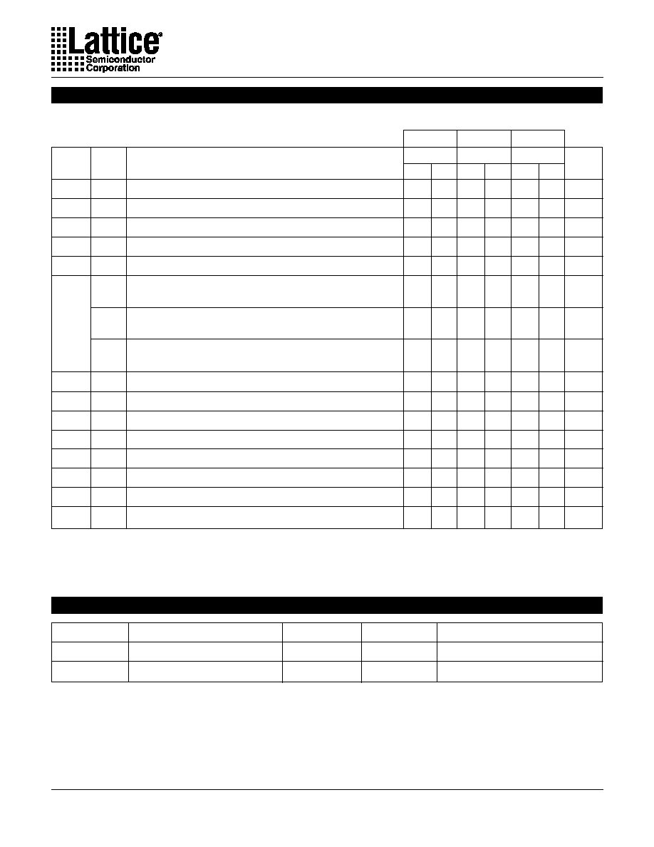
Specifications
GAL22V10
2
Commercial Grade Specifications
Industrial Grade Specifications
Blank = Commercial
I = Industrial
Grade
Package
Power
L = Low Power
Q = Quarter Power
Speed (ns)
XXXXXXXX
XX
X
X X
Device Name
_
P = Plastic DIP
J = PLCC
S = SOIC
GAL22V10D
GAL22V10 Ordering Information
Part Number Description
)
s
n
(
d
p
T
)
s
n
(
u
s
T
)
s
n
(
o
c
T
)
A
m
(
c
c
I
#
g
n
i
r
e
d
r
O
e
g
a
k
c
a
P
5
.
7
5
5
.
4
0
6
1
0
1
V
2
2
L
A
G
D
I
P
L
7
-
P
I
D
c
i
t
s
a
l
P
n
i
P
-
4
2
5
.
4
5
.
4
0
6
1
0
1
V
2
2
L
A
G
D
I
J
L
7
-
C
C
L
P
d
a
e
L
-
8
2
0
1
7
7
0
6
1
0
1
V
2
2
L
A
G
D
I
P
L
0
1
-
P
I
D
c
i
t
s
a
l
P
n
i
P
-
4
2
0
6
1
0
1
V
2
2
L
A
G
D
I
J
L
0
1
-
C
C
L
P
d
a
e
L
-
8
2
5
1
0
1
8
0
5
1
G
I
P
L
5
1
-
D
0
1
V
2
2
L
A
P
I
D
c
i
t
s
a
l
P
n
i
P
-
4
2
0
5
1
I
J
L
5
1
-
D
0
1
V
2
2
L
A
G
C
C
L
P
d
a
e
L
-
8
2
0
2
4
1
0
1
0
5
1
I
P
L
0
2
-
D
0
1
V
2
2
L
A
G
P
I
D
c
i
t
s
a
l
P
n
i
P
-
4
2
0
5
1
I
J
L
0
2
-
D
0
1
V
2
2
L
A
G
C
C
L
P
d
a
e
L
-
8
2
5
2
5
1
5
1
0
5
1
I
P
L
5
2
-
D
0
1
V
2
2
L
A
G
P
I
D
c
i
t
s
a
l
P
n
i
P
-
4
2
0
5
1
I
J
L
5
2
-
D
0
1
V
2
2
L
A
G
C
C
L
P
d
a
e
L
-
8
2
)
s
n
(
d
p
T
)
s
n
(
u
s
T
)
s
n
(
o
c
T
)
A
m
(
c
c
I
#
g
n
i
r
e
d
r
O
e
g
a
k
c
a
P
4
5
.
2
5
.
3
0
4
1
J
L
4
-
D
0
1
V
2
2
L
A
G
C
C
L
P
d
a
e
L
-
8
2
5
3
4
0
4
1
J
L
5
-
D
0
1
V
2
2
L
A
G
C
C
L
P
d
a
e
L
-
8
2
5
.
7
5
.
4
5
.
4
0
4
1
P
L
7
-
D
0
1
V
2
2
L
A
G
P
I
D
c
i
t
s
a
l
P
n
i
P
-
4
2
5
.
4
5
.
4
0
4
1
J
L
7
-
D
0
1
V
2
2
L
A
G
C
C
L
P
d
a
e
L
-
8
2
0
1
7
7
5
5
P
Q
0
1
-
D
0
1
V
2
2
L
A
G
P
I
D
c
i
t
s
a
l
P
n
i
P
-
4
2
5
5
J
Q
0
1
-
D
0
1
V
2
2
L
A
G
C
C
L
P
d
a
e
L
-
8
2
0
3
1
P
L
0
1
-
D
0
1
V
2
2
L
A
G
P
I
D
c
i
t
s
a
l
P
n
i
P
-
4
2
0
3
1
J
L
0
1
-
D
0
1
V
2
2
L
A
G
C
C
L
P
d
a
e
L
-
8
2
0
3
1
S
L
0
1
-
D
0
1
V
2
2
L
A
G
C
I
O
S
n
i
P
-
4
2
5
1
0
1
8
5
5
P
Q
5
1
-
D
0
1
V
2
2
L
A
G
P
I
D
c
i
t
s
a
l
P
n
i
P
-
4
2
5
5
J
Q
5
1
-
D
0
1
V
2
2
L
A
G
C
C
L
P
d
a
e
L
-
8
2
0
3
1
P
L
5
1
-
D
0
1
V
2
2
L
A
G
P
I
D
c
i
t
s
a
l
P
n
i
P
-
4
2
0
3
1
J
L
5
1
-
D
0
1
V
2
2
L
A
G
C
C
L
P
d
a
e
L
-
8
2
0
3
1
S
L
5
1
-
D
0
1
V
2
2
L
A
G
C
I
O
S
n
i
P
-
4
2
5
2
5
1
5
1
5
5
P
Q
5
2
-
D
0
1
V
2
2
L
A
G
P
I
D
c
i
t
s
a
l
P
n
i
P
-
4
2
5
5
J
Q
5
2
-
D
0
1
V
2
2
L
A
G
C
C
L
P
d
a
e
L
-
8
2
0
9
P
L
5
2
-
D
0
1
V
2
2
L
A
G
p
i
D
c
i
t
s
a
l
P
n
i
P
-
4
2
0
9
J
L
5
2
-
D
0
1
V
2
2
L
A
G
C
C
L
P
d
a
e
L
-
8
2
0
9
S
L
5
2
-
D
0
1
V
2
2
L
A
G
C
I
O
S
n
i
P
-
4
2
Specifications
GAL22V10
3
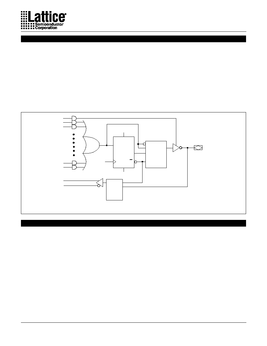
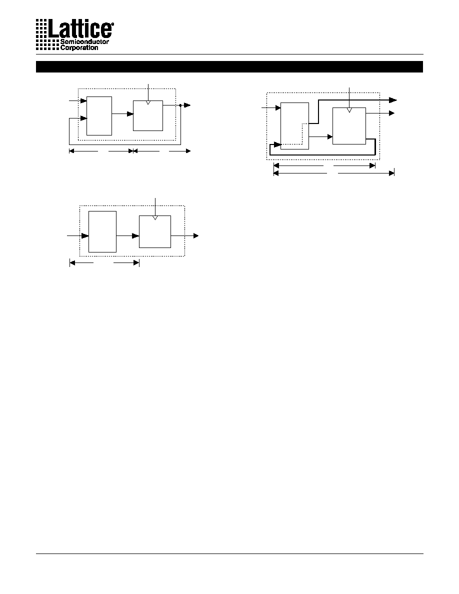
GAL22V10 OUTPUT LOGIC MACROCELL (OLMC)
Each of the Macrocells of the GAL22V10 has two primary functional
modes: registered, and combinatorial I/O. The modes and the
output polarity are set by two bits (SO and S1), which are normally
controlled by the logic compiler. Each of these two primary modes,
and the bit settings required to enable them, are described below
and on the following page.
REGISTERED
In registered mode the output pin associated with an individual
OLMC is driven by the Q output of that OLMC's D-type flip-flop.
Logic polarity of the output signal at the pin may be selected by
specifying that the output buffer drive either true (active high) or
inverted (active low). Output tri-state control is available as an in-
dividual product-term for each OLMC, and can therefore be defined
by a logic equation. The D flip-flop's /Q output is fed back into the
AND array, with both the true and complement of the feedback
available as inputs to the AND array.
NOTE: In registered mode, the feedback is from the /Q output of
the register, and not from the pin; therefore, a pin defined as reg-
istered is an output only, and cannot be used for dynamic
I/O, as can the combinatorial pins.
COMBINATORIAL I/O
In combinatorial mode the pin associated with an individual OLMC
is driven by the output of the sum term gate. Logic polarity of the
output signal at the pin may be selected by specifying that the output
buffer drive either true (active high) or inverted (active low). Out-
put tri-state control is available as an individual product-term for
each output, and may be individually set by the compiler as either
"on" (dedicated output), "off" (dedicated input), or "product-term
driven" (dynamic I/O). Feedback into the AND array is from the pin
side of the output enable buffer. Both polarities (true and inverted)
of the pin are fed back into the AND array.
The GAL22V10 has a variable number of product terms per OLMC.
Of the ten available OLMCs, two OLMCs have access to eight
product terms (pins 14 and 23, DIP pinout), two have ten product
terms (pins 15 and 22), two have twelve product terms (pins 16 and
21), two have fourteen product terms (pins 17 and 20), and two
OLMCs have sixteen product terms (pins 18 and 19). In addition
to the product terms available for logic, each OLMC has an addi-
tional product-term dedicated to output enable control.
The output polarity of each OLMC can be individually programmed
to be true or inverting, in either combinatorial or registered mode.
This allows each output to be individually configured as either active
high or active low.
The GAL22V10 has a product term for Asynchronous Reset (AR)
and a product term for Synchronous Preset (SP). These two prod-
uct terms are common to all registered OLMCs. The Asynchronous
Reset sets all registers to zero any time this dedicated product term
is asserted. The Synchronous Preset sets all registers to a logic
one on the rising edge of the next clock pulse after this product term
is asserted.
NOTE: The AR and SP product terms will force the Q output of the
flip-flop into the same state regardless of the polarity of the output.
Therefore, a reset operation, which sets the register output to a zero,
may result in either a high or low at the output pin, depending on
the pin polarity chosen.
A R
S P
D
Q
Q
C L K
4 T O 1
M U X
2 T O 1
M U X
Output Logic Macrocell (OLMC)
Output Logic Macrocell Configurations
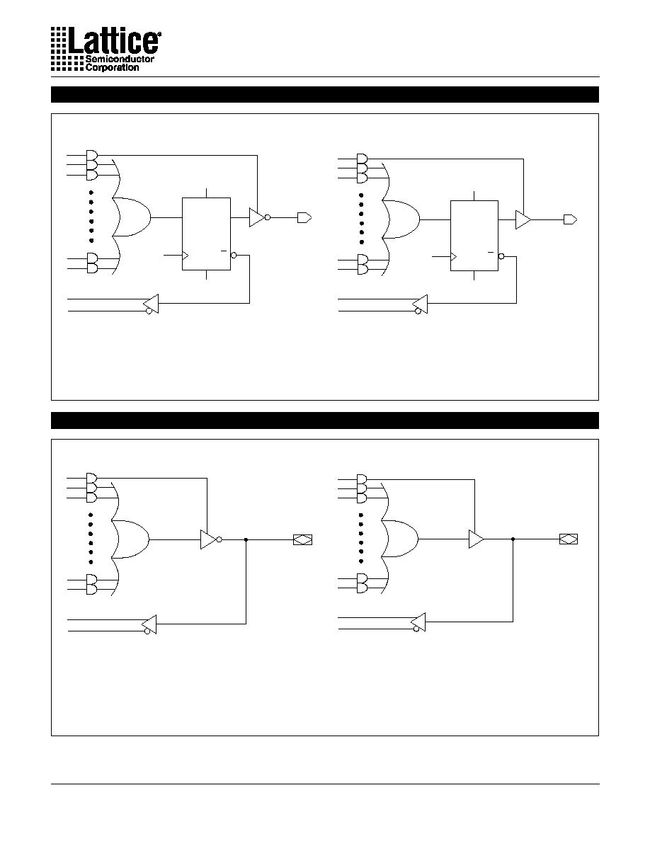
Specifications
GAL22V10
4
ACTIVE HIGH
ACTIVE LOW
ACTIVE HIGH
ACTIVE LOW
S
0
= 1
S
1
= 1
S
0
= 0
S
1
= 1
S
0
= 0
S
1
= 0
S
0
= 1
S
1
= 0
A R
S P
D
Q
Q
C L K
A R
S P
D
Q
Q
C L K
Registered Mode
Combinatorial Mode
Specifications
GAL22V10
5
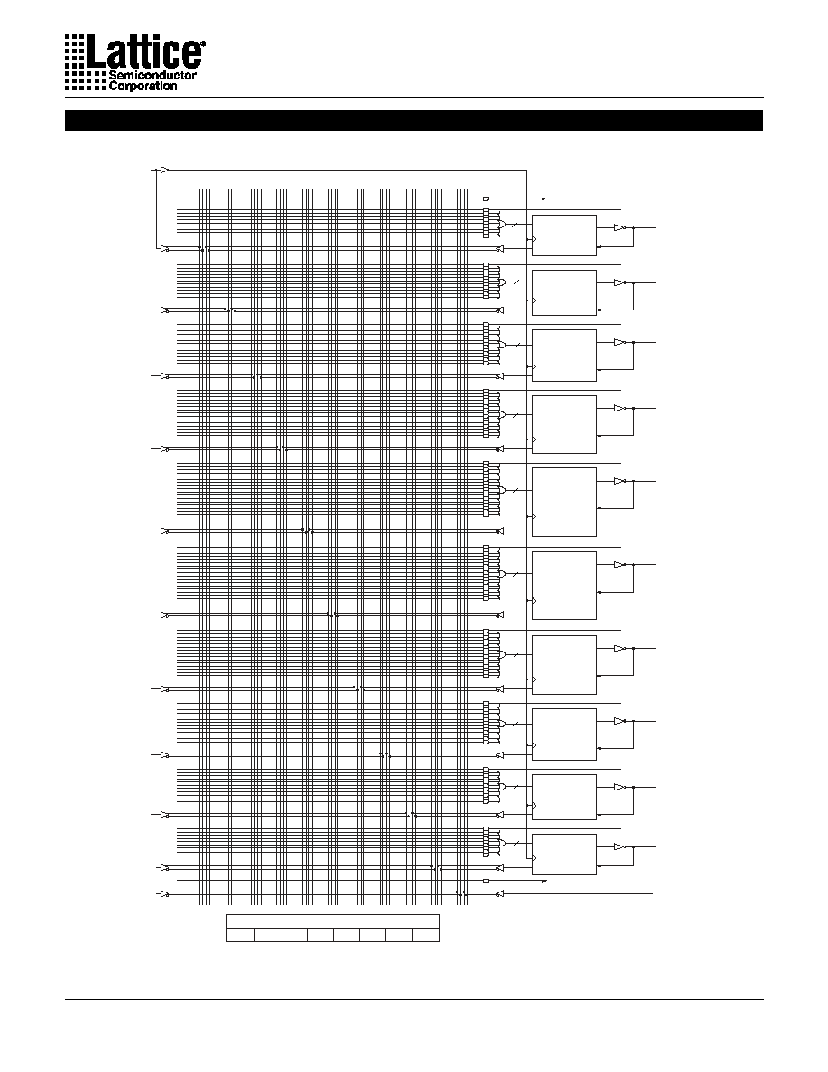
DIP (PLCC) Package Pinouts
1 (2)
22 (26)
OLMC
S0
5810
S1
5811
0440
.
.
.
.
0880
2 (3)
ASYNCHRONOUS RESET
(TO ALL REGISTERS)
0
4
8
12
16
20
24
28
32
36
40
SYNCHRONOUS PRESET
(TO ALL REGISTERS)
10 (12)
0000
5764
0044
.
.
.
0396
23 (27)
S0
5808
S1
5809
21 (25)
OLMC
S0
5812
S1
5813
0924
.
.
.
.
.
1452
3 (4)
4 (5)
5 (6)
20 (24)
OLMC
S0
5814
S1
5815
1496
.
.
.
.
.
.
2112
19 (23)
OLMC
S0
5816
S1
5817
2156
.
.
.
.
.
.
.
2860
18 (21)
OLMC
S0
5818
S1
5819
2904
.
.
.
.
.
.
.
3608
17 (20)
OLMC
S0
5820
S1
5821
3652
.
.
.
.
.
.
4268
OLMC
S0
5822
S1
5823
4312
.
.
.
.
.
4840
8 (10)
16 (19)
15 (18)
OLMC
S0
5824
S1
5825
4884
.
.
.
.
5324
9 (11)
5368
.
.
.
5720
14 (17)
OLMC
S0
5826
S1
5827
7 (9)
6 (7)
11 (13)
13 (16)
8
10
14
16
12
12
16
14
10
8
OLMC
Electronic Signature
5828, 5829 ...
... 5890, 5891
L
S
B
M
S
B
Byte 7 Byte 6 Byte 5 Byte 4
Byte 2 Byte 1 Byte 0
Byte 3
GAL22V10 Logic Diagram / JEDEC Fuse Map
Specifications
GAL22V10
6
Supply voltage V
CC
.......................................
-
0.5 to +7V
Input voltage applied ........................... -2.5 to V
CC
+1.0V
Off-state output voltage applied ........... -2.5 to V
CC
+1.0V
Storage Temperature .................................. -65 to 150
�
C
Ambient Temperature with
Power Applied ......................................... -55 to 125
�
C
1. Stresses above those listed under the "Absolute Maximum
Ratings" may cause permanent damage to the device. These
are stress only ratings and functional operation of the device
at these or at any other conditions above those indicated in
the operational sections of this specification is not implied
(while programming, follow the programming specifications).
Commercial Devices:
Ambient Temperature (T
A
) ............................. 0 to +75
�
C
Supply voltage (V
CC
)
with Respect to Ground ..................... +4.75 to +5.25V
Industrial Devices:
Ambient Temperature (T
A
) ............................ -40 to 85
�
C
Supply voltage (V
CC
)
with Respect to Ground ..................... +4.50 to +5.50V
Specifications
GAL22V10D
COMMERCIAL
I
CC
Operating Power
V
IL
= 0.5V V
IH
= 3.0V
L-4/-5/-7
--
90
140
mA
Supply Current
f
toggle
= 15MHz Outputs Open
L-10
--
90
130
mA
L-15/-25
--
75
90
mA
Q-10/-15/-25
--
45
55
mA
V
IL
Input Low Voltage
Vss � 0.5
--
0.8
V
V
IH
Input High Voltage
2.0
--
Vcc+1
V
I
IL
1
Input or I/O Low Leakage Current
0V
V
IN
V
IL
(MAX.)
--
--
�100
�
A
I
IH
Input or I/O High Leakage Current
3.5V
V
IN
V
CC
--
--
10
�
A
V
OL
Output Low Voltage
I
OL
= MAX. Vin = V
IL
or V
IH
--
--
0.4
V
V
OH
Output High Voltage
I
OH
= MAX. Vin = V
IL
or V
IH
2.4
--
--
V
I
OL
Low Level Output Current
--
--
16
mA
I
OH
High Level Output Current
--
--
�3.2
mA
I
OS
2
Output Short Circuit Current
V
CC
= 5V
V
OUT
= 0.5V T
A
= 25
�
C
�30
--
�130
mA
Over Recommended Operating Conditions (Unless Otherwise Specified)
SYMBOL
PARAMETER
CONDITION
MIN.
TYP.
3
MAX.
UNITS
INDUSTRIAL
I
CC
Operating Power
V
IL
= 0.5V V
IH
= 3.0V
L-7/-10
--
90
160
mA
Supply Current
f
toggle
= 15MHz Outputs Open
L-15/-20/-25
--
75
130
mA
1) The leakage current is due to the internal pull-up on all pins. See Input Buffer section for more information.
2) One output at a time for a maximum duration of one second. Vout = 0.5V was selected to avoid test problems caused by tester
ground degradation. Characterized but not 100% tested.
3) Typical values are at Vcc = 5V and T
A
= 25
�
C
Absolute Maximum Ratings
1
Recommended Operating Conditions
DC Electrical Characteristics
Specifications
GAL22V10
7
t
pd
A
Input or I/O to Combinatorial Output
1
4
1
5
1
7.5
ns
t
co
A
Clock to Output Delay
1
3.5
1
4
1
4.5
ns
t
cf
2
--
Clock to Feedback Delay
--
2.5
--
3
--
3
ns
t
su
--
Setup Time, Input or Fdbk before Clk
2.5
--
3
--
4.5
--
ns
t
h
--
Hold Time, Input or Fdbk after Clk
0
--
0
--
0
--
ns
A
Maximum Clock Frequency with
167
--
142.8
--
111
--
MHz
External Feedback, 1/(tsu + tco)
f
max
3
A
Maximum Clock Frequency with
200
--
166
--
133
--
MHz
Internal Feedback, 1/(tsu + tcf)
A
Maximum Clock Frequency with
250
--
200
--
166
--
MHz
No Feedback
t
wh
--
Clock Pulse Duration, High
2
--
2.5
--
3
--
ns
t
wl
--
Clock Pulse Duration, Low
2
--
2.5
--
3
--
ns
t
en
B
Input or I/O to Output Enabled
1
5
1
6
1
7.5
ns
t
dis
C
Input or I/O to Output Disabled
1
5
1
5.5
1
7.5
ns
t
ar
A
Input or I/O to Asynch. Reset of Reg.
1
4.5
1
5.5
1
9
ns
t
arw
--
Asynch. Reset Pulse Duration
4.5
--
4.5
--
7
--
ns
t
arr
--
Asynch. Reset to Clk
Recovery Time
3
--
4
--
5
--
ns
t
spr
--
Synch. Preset to Clk
Recovery Time
3
--
4
--
5
--
ns
Over Recommended Operating Conditions
UNITS
1) Refer to Switching Test Conditions section.
2) Calculated from fmax with internal feedback. Refer to fmax Description section.
3) Refer to fmax Description section. Characterized initially and after any design or process changes that may affect these
parameters.
PARAM
TEST
COND.
1
DESCRIPTION
SYMBOL
PARAMETER
MAXIMUM*
UNITS
TEST CONDITIONS
C
I
Input Capacitance
8
pF
V
CC
= 5.0V, V
I
= 2.0V
C
I/O
I/O Capacitance
8
pF
V
CC
= 5.0V, V
I/O
= 2.0V
*Characterized but not 100% tested.
-5
MIN. MAX.
COM/IND
COM
-7
MIN. MAX.
AC Switching Characteristics
Capacitance (T
A
= 25
�
C, f = 1.0 MHz)
Specifications
GAL22V10D
COM
-4
MIN. MAX.

Specifications
GAL22V10
8
t
pd
A
Input or I/O to Comb. Output
1
10
3
15
3
20
3
25
ns
t
co
A
Clock to Output Delay
1
7
2
8
2
10
2
15
ns
t
cf
2
--
Clock to Feedback Delay
--
2.5
--
2.5
--
8
--
13
ns
t
su
--
Setup Time, Input or Fdbk before Clk
6
--
10
--
12
--
15
--
ns
t
h
--
Hold Time, Input or Fdbk after Clk
0
--
0
--
0
--
0
--
ns
A
Maximum Clock Frequency with
83.3
--
55.5
--
41.6
--
33.3
--
MHz
External Feedback, 1/(tsu + tco)
f
max
3
A
Maximum Clock Frequency with
110
--
80
--
45.4
--
35.7
--
MHz
Internal Feedback, 1/(tsu + tcf)
A
Maximum Clock Frequency with
125
--
83.3
--
50
--
38.5
--
MHz
No Feedback
t
wh
--
Clock Pulse Duration, High
4
--
6
--
10
--
13
--
ns
t
wl
--
Clock Pulse Duration, Low
4
--
6
--
10
--
13
--
ns
t
en
B
Input or I/O to Output Enabled
1
10
3
15
3
20
3
25
ns
t
dis
C
Input or I/O to Output Disabled
1
9
3
15
3
20
3
25
ns
t
ar
A
Input or I/O to Asynch. Reset of Reg.
1
13
3
20
3
25
3
25
ns
t
arw
--
Asynch. Reset Pulse Duration
8
--
15
--
20
--
25
--
ns
t
arr
--
Asynch. Reset to Clk
Recovery Time
8
--
10
--
20
--
25
--
ns
t
spr
--
Synch. Preset to Clk
Recovery Time
8
--
10
--
14
--
15
--
ns
Specifications
GAL22V10D
-10
MIN. MAX.
-25
MIN. MAX.
-20
MIN. MAX.
-15
MIN. MAX.
Over Recommended Operating Conditions
UNITS
1) Refer to Switching Test Conditions section.
2) Calculated from fmax with internal feedback. Refer to fmax Description section.
3) Refer to fmax Description section.
SYMBOL
PARAMETER
MAXIMUM*
UNITS
TEST CONDITIONS
C
I
Input Capacitance
8
pF
V
CC
= 5.0V, V
I
= 2.0V
C
I/O
I/O Capacitance
8
pF
V
CC
= 5.0V, V
I/O
= 2.0V
*Characterized but not 100% tested.
PARAM.
TEST
COND.
1
DESCRIPTION
COM / IND
IND
COM / IND
COM / IND
Capacitance (T
A
= 25
�
C, f = 1.0 MHz)
AC Switching Characteristics

Specifications
GAL22V10
9
Input or I/O to Output Enable/Disable
Registered Output
Combinatorial Output
VALID INPUT
INPUT or
I/O FEEDBACK
t
pd
COMBINATORIAL
OUTPUT
INPUT or
I/O FEEDBACK
REGISTERED
OUTPUT
CLK
VALID INPUT
t
su
t
co
t
h
(external fdbk)
1/
f
max
t
en
t
dis
INPUT or
I/O FEEDBACK
OUTPUT
CLK
(w/o fdbk)
t
w h
t
w l
1 /
f
m a x
Clock Width
REGISTERED
OUTPUT
CLK
INPUT or
I/O FEEDBACK
DRIVING SP
t
su
t
h
t
co
t
spr
R E G I S T ER E D
O U T P U T
CLK
t
arw
t
ar
t
arr
INPU T or
I/O F EED B ACK
DRIVI NG AR
f
max with Feedback
Asynchronous Reset
Synchronous Preset
CLK
REGISTERED
FEEDBACK
t
cf
t
su
1/
f
max (internal fdbk)
Switching Waveforms
Specifications
GAL22V10
10
f
max with Internal Feedback 1/(
t
su+
t
cf)
Note: fmax with external feedback is cal-
culated from measured tsu and tco.
f
max with External Feedback 1/(
t
su+
t
co)
Note: tcf is a calculated value, derived by sub-
tracting tsu from the period of fmax w/internal
feedback (tcf = 1/fmax - tsu). The value of tcf is
used primarily when calculating the delay from
clocking a register to a combinatorial output
(through registered feedback), as shown above.
For example, the timing from clock to a combi-
natorial output is equal to tcf + tpd.
f
max with No Feedback
Note: fmax with no feedback may be less
than 1/(twh + twl). This is to allow for a
clock duty cycle of other than 50%.
R E G I S T E R
L O G I C
A R R A Y
t
c o
t
s u
C L K
REGISTER
LOGIC
ARRAY
CLK
t
su +
t
h
CLK
REGISTER
LOGIC
ARRAY
t
cf
t
pd
fmax Descriptions
Specifications
GAL22V10
11
GAL22V10D-4 Output Load Conditions (see figure below)
Test Condition
R
1
C
L
A
50
50pF
B
Z to Active High at 1.9V
50
50pF
Z to Active Low at 1.0V
50
50pF
C
Active High to Z at 1.9V
50
50pF
Active Low to Z at 1.0V
50
50pF
Input Pulse Levels
GND to 3.0V
Input Rise and
D-4/-5/-7
1.5ns 10% � 90%
Fall Times
D-10/-15/-20/-25
2.0ns 10% � 90%
Input Timing Reference Levels
1.5V
Output Timing Reference Levels
1.5V
Output Load
See Figure
3-state levels are measured 0.5V from steady-state active
level.
TEST POINT
C *
L
FROM OUTPUT (O/Q)
UNDER TEST
+5V
*C
L
INCLUDES TEST FIXTURE AND PROBE CAPACITANCE
R
2
R
1
Output Load Conditions (except D-4) (see figure below)
Test Condition
R
1
R
2
C
L
A
300
390
50pF
B
Active High
390
50pF
Active Low
300
390
50pF
C
Active High
390
5pF
Active Low
300
390
5pF
TEST POINT
Z
0
= 50
, C
L
*
FROM OUTPUT (O/Q)
UNDER TEST
+1.45V
R
1
Switching Test Conditions
Specifications
GAL22V10
12
Electronic Signature
An electronic signature (ES) is provided in every GAL22V10
device. It contains 64 bits of reprogrammable memory that can
contain user-defined data. Some uses include user ID codes,
revision numbers, or inventory control. The signature data is
always available to the user independent of the state of the se-
curity cell.
The electronic signature is an additional feature not present in
other manufacturers' 22V10 devices. To use the extra feature of
the user-programmable electronic signature it is necessary to
choose a Lattice Semiconductor 22V10 device type when com-
piling a set of logic equations. In addition, many device program-
mers have two separate selections for the device, typically a
GAL22V10 and a GAL22V10-UES (UES = User Electronic Sig-
nature) or GAL22V10-ES. This allows users to maintain compat-
ibility with existing 22V10 designs, while still having the option to
use the GAL device's extra feature.
The JEDEC map for the GAL22V10 contains the 64 extra fuses
for the electronic signature, for a total of 5892 fuses. However,
the GAL22V10 device can still be programmed with a standard
22V10 JEDEC map (5828 fuses) with any qualified device pro-
grammer.
Security Cell
A security cell is provided in every GAL22V10 device to prevent
unauthorized copying of the array patterns. Once programmed,
this cell prevents further read access to the functional bits in the
device. This cell can only be erased by re-programming the
device, so the original configuration can never be examined once
this cell is programmed. The Electronic Signature is always avail-
able to the user, regardless of the state of this control cell.
Latch-Up Protection
GAL22V10 devices are designed with an on-board charge pump
to negatively bias the substrate. The negative bias is of sufficient
magnitude to prevent input undershoots from causing the circuitry
to latch. Additionally, outputs are designed with n-channel pullups
instead of the traditional p-channel pullups to eliminate any pos-
sibility of SCR induced latching.
Device Programming
GAL devices are programmed using a Lattice Semiconductor-
approved Logic Programmer, available from a number of manu-
facturers (see the the GAL Development Tools section). Com-
plete programming of the device takes only a few seconds. Eras-
ing of the device is transparent to the user, and is done automati-
cally as part of the programming cycle.
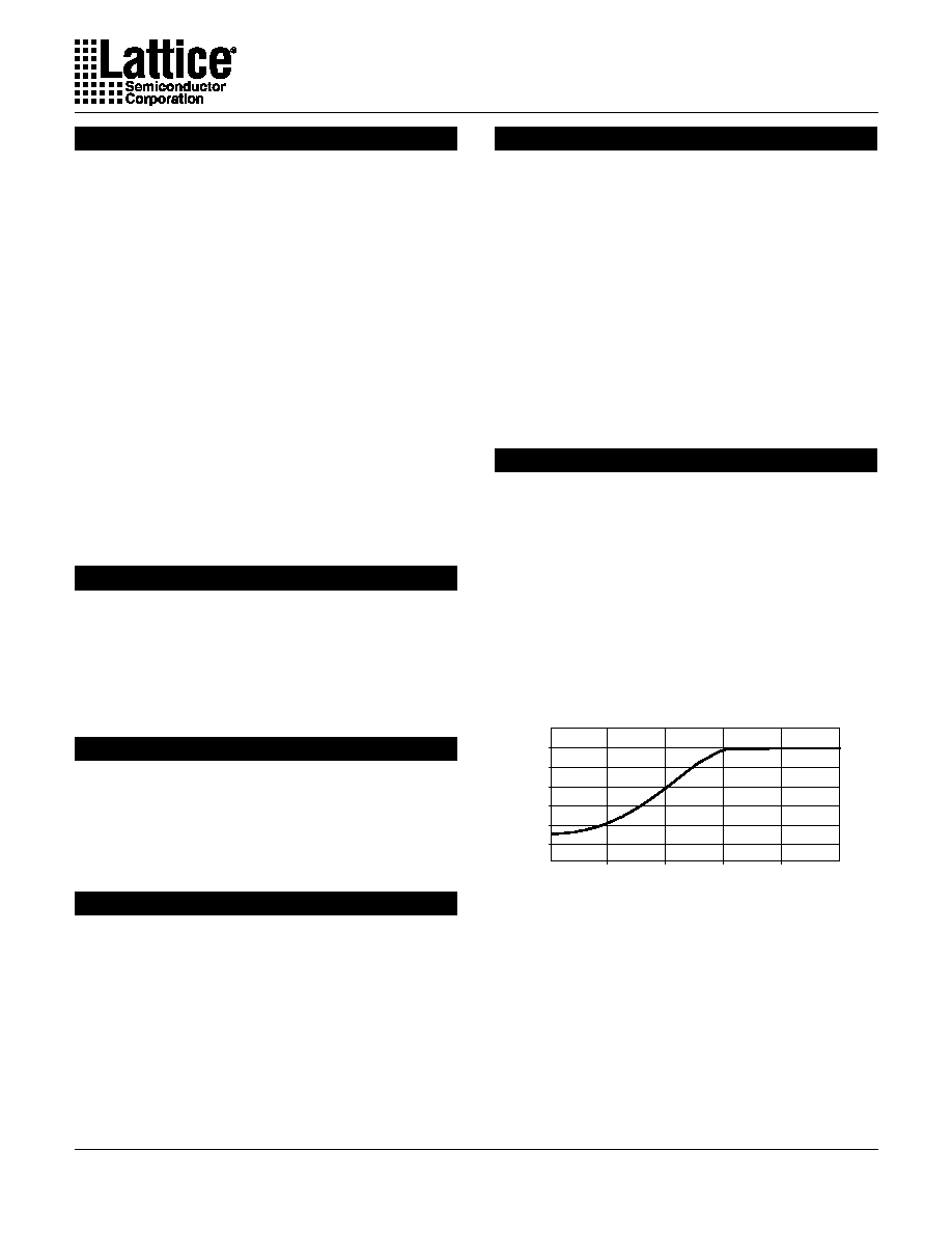
Typical Input Current
1 . 0
2 . 0
3 . 0
4 . 0
5 . 0
- 6 0
0
- 2 0
- 4 0
0
In p u t V o lt ag e ( V o lt s)
I
nput
C
u
r
r
e
nt
(
u
A
)
Output Register Preload
When testing state machine designs, all possible states and state
transitions must be verified in the design, not just those required
in the normal machine operations. This is because certain events
may occur during system operation that throw the logic into an
illegal state (power-up, line voltage glitches, brown-outs, etc.). To
test a design for proper treatment of these conditions, a way must
be provided to break the feedback paths, and force any desired
(i.e., illegal) state into the registers. Then the machine can be
sequenced and the outputs tested for correct next state condi-
tions.
The GAL22V10 device includes circuitry that allows each regis-
tered output to be synchronously set either high or low. Thus, any
present state condition can be forced for test sequencing. If
necessary, approved GAL programmers capable of executing test
vectors perform output register preload automatically.
Input Buffers
GAL22V10 devices are designed with TTL level compatible in-
put buffers. These buffers have a characteristically high imped-
ance, and present a much lighter load to the driving logic than bi-
polar TTL devices.
The input and I/O pins also have built-in active pull-ups. As a re-
sult, floating inputs will float to a TTL high (logic 1). However,
Lattice Semiconductor recommends that all unused inputs and
tri-stated I/O pins be connected to an adjacent active input, Vcc,
or ground. Doing so will tend to improve noise immunity and
reduce Icc for the device. (See equivalent input and I/O schemat-
ics on the following page.)

Specifications
GAL22V10
13
(Vref Typical = 3.2V)
(Vref Typical = 3.2V)
Circuitry within the GAL22V10 provides a reset signal to all reg-
isters during power-up. All internal registers will have their Q out-
puts set low after a specified time (tpr, 1
�
s MAX). As a result, the
state on the registered output pins (if they are enabled) will be
either high or low on power-up, depending on the programmed
polarity of the output pins. This feature can greatly simplify state
machine design by providing a known state on power-up. The
timing diagram for power-up is shown below. Because of the asyn-
chronous nature of system power-up, some conditions must be
met to guarantee a valid power-up reset of the GAL22V10. First,
the Vcc rise must be monotonic. Second, the clock input must
be at static TTL level as shown in the diagram during power up.
The registers will reset within a maximum of tpr time. As in nor-
mal system operation, avoid clocking the device until all input and
feedback path setup times have been met. The clock must also
meet the minimum pulse width requirements.
Vcc
PIN
Vcc
Vref
Active Pull-up
Circuit
ESD
Protection
Circuit
ESD
Protection
Circuit
Vcc
PIN
Vcc (min.)
t
pr
Internal Register
Reset to Logic "0"
Device Pin
Reset to Logic "1"
t
wl
t
su
Device Pin
Reset to Logic "0"
V c c
C L K
INTERNAL REGISTER
Q - OUTPUT
ACTIVE LOW
OUTPUT REGISTER
ACTIVE HIGH
OUTPUT REGISTER
Vcc
PIN
Vref
Tri-State
Control
Active Pull-up
Circuit
Feedback
(To Input Buffer)
PIN
Feedback
Data
Output
Typical Input
Typical Output
Power-Up Reset
Input/Output Equivalent Schematics
Specifications
GAL22V10
14
Delta Tpd vs # of Outputs
Switching
-0.3
-0.2
-0.1
0
1
2
3
4
5
6
7
8
9
1 0
Number of Outputs Switching
Delta T
pd (
ns)
RISE
FALL
Delta Tco vs # of Outputs
Switching
-0.4
-0.3
-0.2
-0.1
0
1
2
3
4
5
6
7
8
9
1 0
Number of Outputs Switching
Delta T
co (
ns)
Delta T
co (
ns)
RISE
FALL
Delta Tpd vs Output Loading
Output Loading (pF)
Delta T
pd (
ns)
RISE
FALL
Delta Tco vs Output Loading
RISE
FALL
Normalized Tpd vs Vcc
Normalized T
p
d
Normalized T
p
d
RISE
FALL
Normalized Tco vs Vcc
RISE
FALL
Normalized Tsu vs Vcc
Supply Voltage (V)
Supply Voltage (V)
Supply Voltage (V)
RISE
FALL
Normalized Tpd vs Temp
Normalized Tco vs Temp
Normalized Tsu vs Temp
125
100
75
50
25
0
-25
-55
125
100
75
50
25
0
-25
-55
300
250
200
150
100
50
0
Output Loading (pF)
300
250
200
150
100
50
0
Temperature (deg. C)
Temperature (deg. C)
Temperature (deg. C)
125
100
75
50
25
0
-25
-55
RISE
FALL
RISE
FALL
RISE
FALL
5.5
5.25
5
4.75
4.5
0.9
1.3
1.2
1.1
1
0.9
0.8
12
8
4
0
-4
12
8
4
0
-4
1.3
1.2
1.1
1
0.9
0.8
0.9
1
1.1
1.2
0.95
1
1.05
1.1
Normalized T
c
o
Normalized T
c
o
0.9
0.95
1
1.05
1.1
Normalized T
Normalized T
s
u
0.9
0.95
1
1.05
1.1
5.5
5.25
5
4.75
4.5
5.5
5.25
5
4.75
4.5
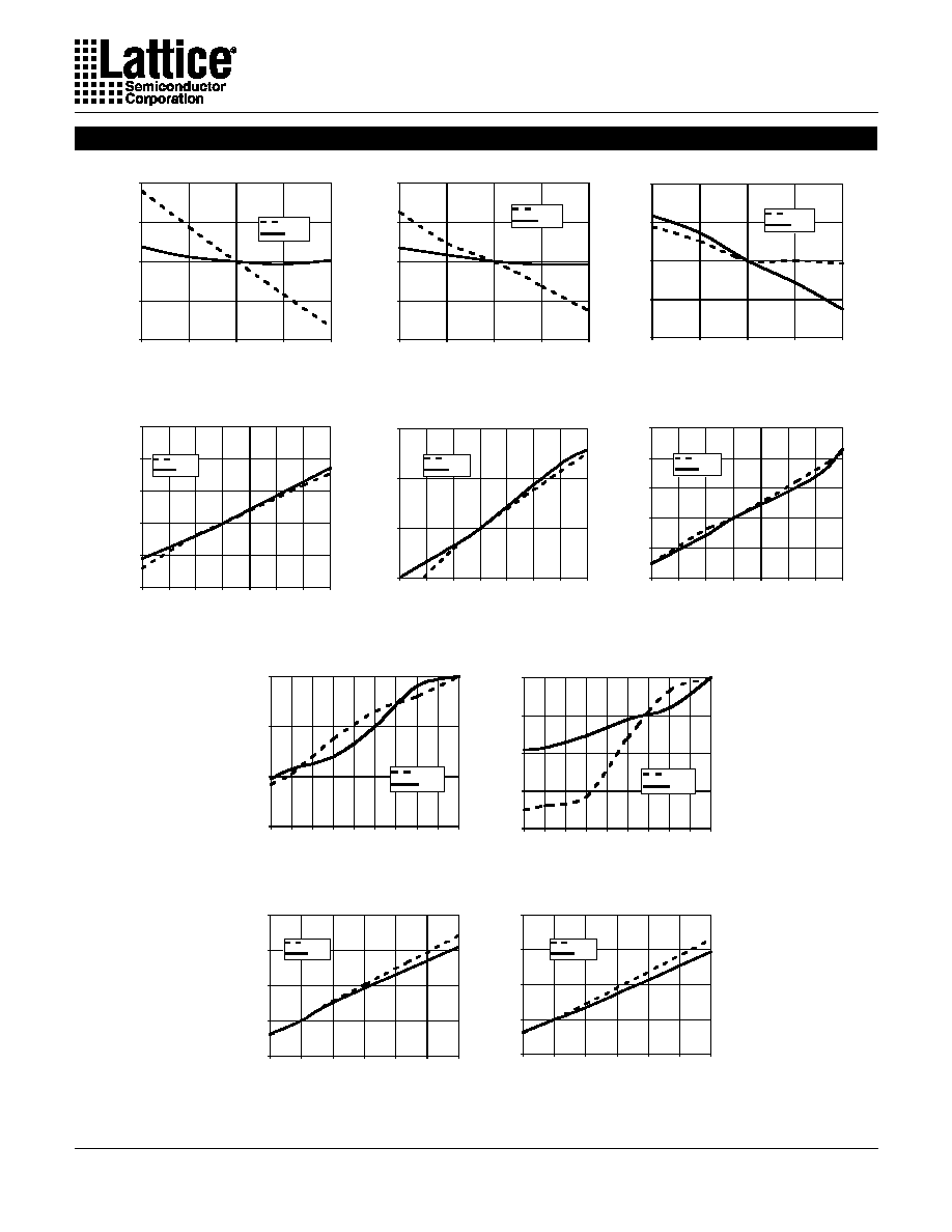
GAL22V10D-4/-5/-7/-10L (PLCC): Typical AC and DC Characteristic Diagrams
Specifications
GAL22V10
15
Vol vs Iol
0
0.2
0.4
0.6
0
5
10
15
20
25
30
35
40
Iol (mA)
Vol (
V
)
Voh vs Ioh
0
1
2
3
4
0
5
10 1 5 2 0 2 5 3 0 3 5 4 0 4 5 50 55 60
Ioh(mA)
Voh (
V
)
Voh vs Ioh
3.15
3.25
3.35
3.45
3.55
3.65
3.75
3.85
3.95
0.00
1.00
2.00
3.00
4.00
5.00
Ioh(mA)
Voh (
V
)
Normalized Icc vs Vcc
0.8
0.9
1
1.1
1.2
4.5
4.75
5
5.25
5.5
Supply Voltage (V)
Normalized I
c
c
Normalized Icc vs Temp
0.7
0.8
0.9
1
1.1
1.2
1.3
-55
-25
0
2 5
5 0
8 8
100
125
Temperature (deg. C)
Normalized I
c
c
Normalized Icc vs Freq
0.95
1
1.05
1.1
1.15
1.2
1
15
25
50
75
1 00
Frequency (MHz)
Normalized I
c
c
Input Clamp (Vik)
Vik (V)
Iik (
mA)
Delta Icc vs Vin (1 input)
6
5
4
3
2
1
0
0
0.5
1
1.5
2
2.5
3
3.5
4
4.5
5
-3
100
80
60
40
20
0
-2.5
-2
-1.5
-1
-0.5
1
Vin (V)
Delta I
cc (
mA)
GAL22V10D-4/-5/-7/-10L (PLCC): Typical AC and DC Characteristic Diagrams
Specifications
GAL22V10
16
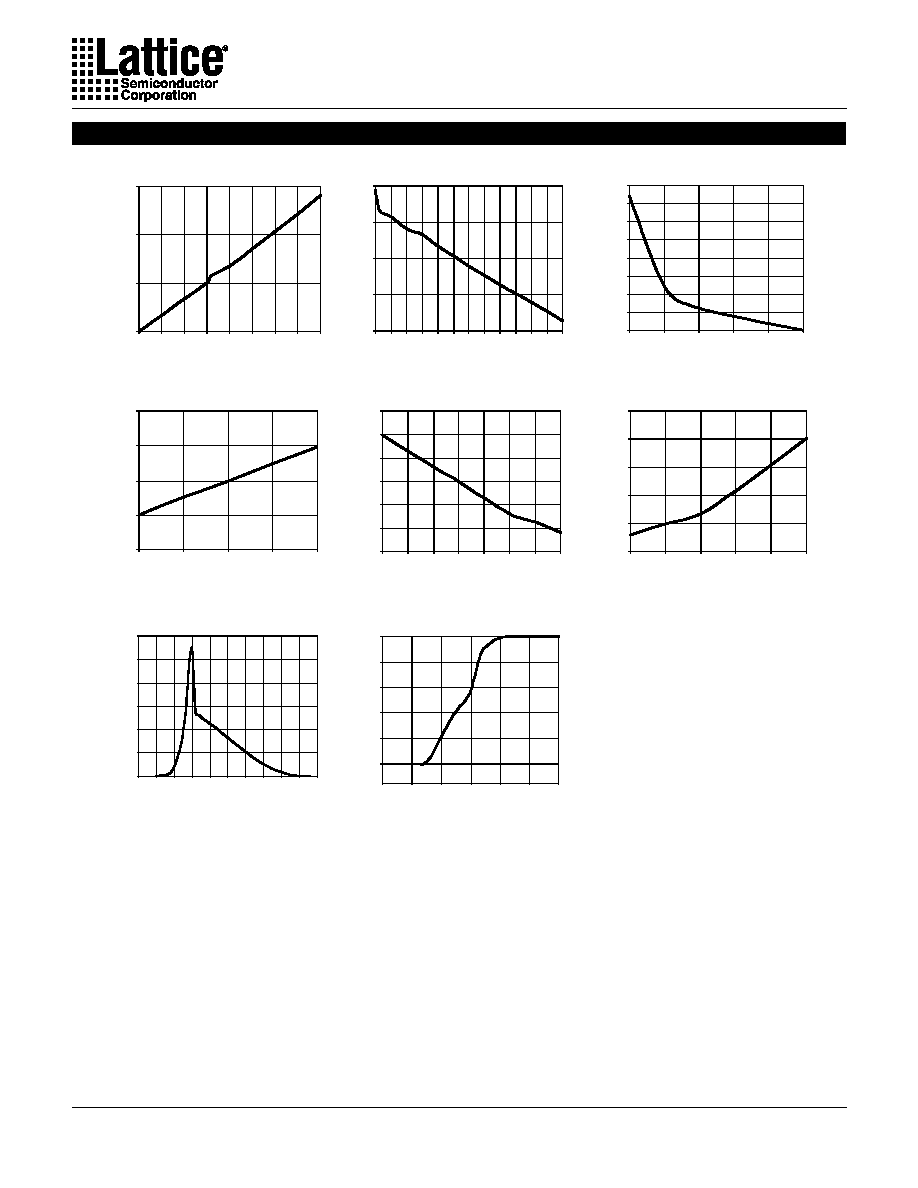
GAL22V10D-7/10L (PDIP): Typical AC and DC Characteristic Diagrams
Normalized Tpd vs Vcc
0.9
0.95
1
1.05
1.1
4.5
4.75
5
5.25
5.5
Supply Voltage (V)
Normalized Tpd
RISE
FALL
Normalized Tco vs Vcc
0.95
1
1.05
1.1
4.5
4.75
5
5.25
5.5
Supply Voltage (V)
Normalized Tco
RISE
FALL
Normalized Tsu vs Vcc
0.8
0.9
1
1.1
1.2
4.5
4.75
5
5.25
5.5
Supply Voltage (V)
Normalized Tsu
RISE
FALL
Normalized Tpd vs Temp
0.8
0.9
1
1.1
1.2
1.3
-55
-25
0
25
50
75
100
125
Temperature (deg. C)
Normalized Tpd
RISE
FALL
Normalized Tsu vs Temp
0.8
0.9
1
1.1
1.2
1.3
-55
-25
0
25
50
75
100
125
Temperature (deg. C)
Normalized Tsu
RISE
FALL
Normalized Tco vs Temp
0.8
0.9
1
1.1
1.2
-55
-25
0
25
50
75
100
125
Temperature (deg. C)
Normalized Tco
RISE
FALL
Delta Tpd vs # of Outputs
Switching
-1.1
-1
-0.9
-0.8
-0.7
-0.6
-0.5
-0.4
-0.3
-0.2
-0.1
0
1
2
3
4
5
6
7
8
9
10
Number of Outputs Switching
Delta Tpd (ns)
RISE
FALL
Delta Tco vs # of Outputs
Switching
-1.1
-1
-0.9
-0.8
-0.7
-0.6
-0.5
-0.4
-0.3
-0.2
-0.1
0
1
2
3
4
5
6
7
8
9
10
Number of Outputs Switching
Delta Tco (ns)
RISE
FALL
Delta Tpd vs Output Loading
-4
0
4
8
12
0
50
100
150
200
250
300
Output Loading (pF)
Delta Tpd (ns)
RISE
FALL
Delta Tco vs Output Loading
-4
0
4
8
12
0
50
100
150
200
250
300
Output Loading (pF)
Delta Tco (ns)
RISE
FALL
Specifications
GAL22V10
17
GAL22V10D-7/10L (PDIP): Typical AC and DC Characteristic Diagrams
Vol vs Iol
0
0.1
0.2
0.3
0.4
0.5
0
5
10
15
20
25
30
Iol (mA)
Vol (V)
Voh vs Ioh
0
1
2
3
4
0
5
10
15
20
25
30
35
40
Ioh (mA)
Voh (V)
Voh vs Ioh
2.8
2.9
3
3.1
3.2
3.3
3.4
3.5
3.6
3.7
3.8
0.00
1.00
2.00
3.00
4.00
5.00
Ioh (mA)
Voh (V)
Normalized Icc vs Vcc
0.85
0.9
0.95
1
1.05
1.1
1.15
4.5
4.75
5
5.25
5.5
Supply Voltage (V)
Normalized Icc
Normalized Icc vs Temp
0.7
0.8
0.9
1
1.1
1.2
1.3
-55
0
25
100
Temperature (deg. C)
Normalized Icc
Normalized Icc vs Freq
0.95
1
1.05
1.1
1.15
1.2
1
15
25
50
75
100
Frequency (MHz)
Normalized Icc
Input Clamp (Vik)
0
10
20
30
40
50
60
70
80
90
100
-2.5
-2
-1.5
-1
-0.5
0
Vik (V)
Iik (mA)
Delta Isb vs Vin (1 input)
0
1
2
3
4
5
6
7
8
9
10
0
0.5
1
1.5
2
2.5
3
3.5
4
4.5
5
Vin (V)
Delta Icc (mA)
Specifications
GAL22V10
18
Normalized Tpd vs Vcc
0.9
0.95
1
1.05
1.1
4.5
4.75
5
5.25
5.5
Supply Voltage (V)
Normalized T
p
d
RISE
FALL
Normalized Tco vs Vcc
0.9
0.95
1
1.05
1.1
1.15
4.5
4.75
5
5.25
5.5
Supply Voltage (V)
Normalized T
c
o
RISE
FALL
Normalized Tsu vs Vcc
0.8
0.9
1
1.1
1.2
4.5
4.75
5
5.25
5.5
Supply Voltage (V)
Normalized T
s
u
RISE
FALL
Normalized Tpd vs Temp
0.8
0.9
1
1.1
1.2
1.3
-55
-25
0
25
50
75
100
125
Temperature (deg. C)
Normalized T
p
d
RISE
FALL
Normalized Tsu vs Temp
0.75
0.85
0.95
1.05
1.15
1.25
1.35
1.45
-55
-25
0
25
50
75
100
1 25
Temperature (deg. C)
Normalized T
s
u
RISE
FALL
Normalized Tco vs Temp
0.8
0.9
1
1.1
1.2
1.3
-55
-25
0
25
50
75
100
1 25
Temperature (deg. C)
Normalized T
c
o
RISE
FALL
Delta Tpd vs # of Outputs
Switching
-1.2
-0.8
-0.4
0
1
2
3
4
5
6
7
8
9
1 0
Number of Outputs Switching
Delta T
pd (
ns)
RISE
FALL
Delta Tco vs # of Outputs
Switching
-1.2
-0.8
-0.4
0
1
2
3
4
5
6
7
8
9
1 0
Number of Outputs Switching
Delta T
co (
ns)
RISE
FALL
Delta Tpd vs Output Loading
-8
-4
0
4
8
1 2
1 6
2 0
0
50
100
150
200
250
3 00
Output Loading (pF)
Delta T
pd (
ns)
RISE
FALL
Delta Tco vs Output Loading
-4
0
4
8
12
16
20
0
50
100
150
200
250
3 00
Output Loading (pF)
Delta T
co (
ns)
RISE
FALL
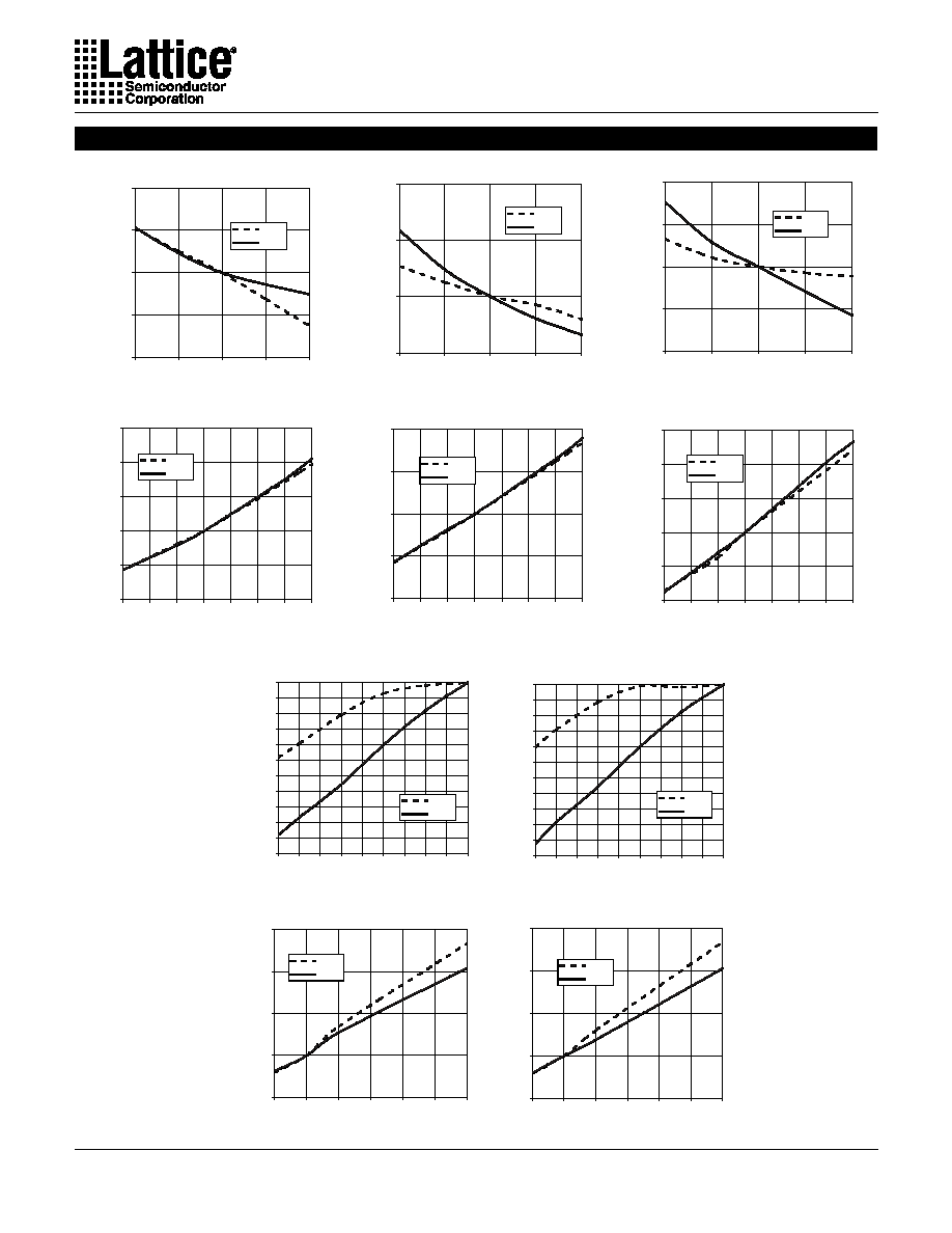
GAL22V10D-10Q and Slower (L & Q): Typical AC and DC Characteristic Diagrams
Specifications
GAL22V10
19
Vol vs Iol
0
0.2
0.4
0.6
0
5
10
15
20
25
30
35
4 0
Iol (mA)
Vol (
V
)
Voh vs Ioh
0
0.5
1
1.5
2
2.5
3
3.5
4
4.5
0
20
40
6 0
Ioh (mA)
Voh (
V
)
Voh vs Ioh
2.5
3
3.5
4
4.5
0.00
1.00
2.00
3.00
4.00
5.00
Ioh (mA)
Voh (
V
)
Normalized Icc vs Vcc
0.8
0.9
1
1.1
1.2
4.5
4.75
5
5.25
5.5
Supply Voltage (V)
Normalized I
c
c
Normalized Icc vs Temp
0.75
0.85
0.95
1.05
1.15
1.25
1.35
-55
-25
0
25
50
88
100
1 25
Temperature (deg. C)
Normalized I
c
c
Normalized Icc vs Freq
0.9
1
1.1
1.2
1.3
1.4
1
15
25
50
75
1 00
Frequency (MHz)
Normalized I
c
c
Input Clamp (Vik)
0
1 0
2 0
3 0
4 0
5 0
6 0
7 0
8 0
9 0
-2.5
-2
-1.5
-1
-0.5
0
Vik (V)
Iik (
m
A)
Delta Icc vs Vin (1 input)
0
1
2
3
4
5
6
7
0
0.5
1
1.5
2
2.5
3
3.5
4
4.5
5
Vin (V)
Delta I
cc (
m
A)
GAL22V10D-10Q and Slower (L & Q): Typical AC and DC Characteristic Diagrams

Specifications
GAL22V10
20
Notes