Document Outline
- Table of Contents
- GAL22V10 Datasheet
- Pin Configuration
- Ordering Information
- 22V10D: DC Electrical Characteristics
- 22V10D: AC Characteristics
- 22V10C: DC Electrical Characteristics
- 22V10C: AC Characteristics
- 22V10B: DC Electrical Characteristics
- 22V10B: AC Characteristics
Specifications
GAL22V10
1
Features
∑ HIGH PERFORMANCE E
2
CMOS
Æ
TECHNOLOGY
-- 4 ns Maximum Propagation Delay
-- Fmax = 250 MHz
-- 3.5 ns Maximum from Clock Input to Data Output
-- UltraMOS
Æ
Advanced CMOS Technology
∑ ACTIVE PULL-UPS ON ALL PINS
∑ COMPATIBLE WITH STANDARD 22V10 DEVICES
-- Fully Function/Fuse-Map/Parametric Compatible
with Bipolar and UVCMOS 22V10 Devices
∑ 50% to 75% REDUCTION IN POWER VERSUS BIPOLAR
-- 90mA Typical Icc on Low Power Device
-- 45mA Typical Icc on Quarter Power Device
∑ E
2
CELL TECHNOLOGY
-- Reconfigurable Logic
-- Reprogrammable Cells
-- 100% Tested/100% Yields
-- High Speed Electrical Erasure (<100ms)
-- 20 Year Data Retention
∑ TEN OUTPUT LOGIC MACROCELLS
-- Maximum Flexibility for Complex Logic Designs
∑ PRELOAD AND POWER-ON RESET OF REGISTERS
-- 100% Functional Testability
∑ APPLICATIONS INCLUDE:
-- DMA Control
-- State Machine Control
-- High Speed Graphics Processing
-- Standard Logic Speed Upgrade
∑ ELECTRONIC SIGNATURE FOR IDENTIFICATION
ESCRIPTION
Description
The GAL22V10, at 4ns maximum propagation delay time, combines
a high performance CMOS process with Electrically Erasable (E
2
)
floating gate technology to provide the highest performance avail-
able of any 22V10 device on the market. CMOS circuitry allows
the GAL22V10 to consume much less power when compared to
bipolar 22V10 devices. E
2
technology offers high speed (<100ms)
erase times, providing the ability to reprogram or reconfigure the
device quickly and efficiently.
The generic architecture provides maximum design flexibility by
allowing the Output Logic Macrocell (OLMC) to be configured by
the user. The GAL22V10 is fully function/fuse map/parametric com-
patible with standard bipolar and CMOS 22V10 devices.
Unique test circuitry and reprogrammable cells allow complete AC,
DC, and functional testing during manufacture. As a result, Lat-
tice Semiconductor delivers 100% field programmability and func-
tionality of all GAL products. In addition, 100 erase/write cycles and
data retention in excess of 20 years are specified.
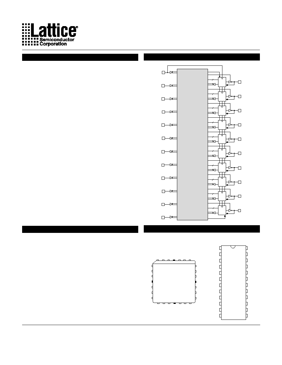
GAL22V10
High Performance E
2
CMOS PLD
Generic Array LogicTM
PROGRAMMABLE
AND-ARRAY
(132X44)
I/O/Q
I/O/Q
I/O/Q
I/O/Q
I/O/Q
I/O/Q
I/O/Q
I/O/Q
I/O/Q
I/O/Q
I
I/CLK
I
I
I
I
I
I
I
I
I
I
RESET
PRESET
8
10
12
14
16
16
14
12
10
8
OLMC
OLMC
OLMC
OLMC
OLMC
OLMC
OLMC
OLMC
OLMC
OLMC
Copyright © 2000 Lattice Semiconductor Corp. All brand or product names are trademarks or registered trademarks of their respective holders. The specifications and information herein are subject
to change without notice.
LATTICE SEMICONDUCTOR CORP., 5555 Northeast Moore Ct., Hillsboro, Oregon 97124, U.S.A.
August 2000
Tel. (503) 268-8000; 1-800-LATTICE; FAX (503) 268-8556; http://www.latticesemi.com
GAL22V10
Top View
PLCC
1
12
13
24
I/CLK
I
I
I
I
I
I
I
I
I
I
GND
Vcc
I/O/Q
I/O/Q
I/O/Q
I/O/Q
I/O/Q
I/O/Q
I/O/Q
I/O/Q
I/O/Q
I/O/Q
I
6
18
GAL
22V10
2
28
NC
I/CLK
I
I
I
I
I
I
I
I
NC
NC
NC
GND
I
I
I
I/O/Q
I/O/Q
I/O/Q
I/O/Q
I/O/Q
I/O/Q
I/O/Q
Vcc
I/O/Q
I/O/Q
I/O/Q
4
26
25
19
18
21
23
16
14
12
11
9
7
5
DIP
22v10_06
Functional Block Diagram
Pin Configuration
Specifications
GAL22V10
2
)
s
n
(
d
p
T
)
s
n
(
u
s
T
)
s
n
(
o
c
T
)
A
m
(
c
c
I
#
g
n
i
r
e
d
r
O
e
g
a
k
c
a
P
4
5
.
2
5
.
3
0
4
1
J
L
4
-
D
0
1
V
2
2
L
A
G
C
C
L
P
d
a
e
L
-
8
2
5
3
4
0
4
1
J
L
5
-
D
0
1
V
2
2
L
A
G
C
C
L
P
d
a
e
L
-
8
2
0
5
1
J
L
5
-
C
0
1
V
2
2
L
A
G
C
C
L
P
d
a
e
L
-
8
2
5
.
7
5
.
4
5
.
4
0
4
1
P
L
7
-
D
0
1
V
2
2
L
A
G
P
I
D
c
i
t
s
a
l
P
n
i
P
-
4
2
5
5
.
4
0
4
1
P
L
7
-
C
0
1
V
2
2
L
A
G
P
I
D
c
i
t
s
a
l
P
n
i
P
-
4
2
5
.
4
5
.
4
0
4
1
J
L
7
-
C
0
1
V
2
2
L
A
G
r
o
J
L
7
-
D
0
1
V
2
2
L
A
G
C
C
L
P
d
a
e
L
-
8
2
5
.
6
5
0
4
1
P
L
7
-
B
0
1
V
2
2
L
A
G
P
I
D
c
i
t
s
a
l
P
n
i
P
-
4
2
0
4
1
J
L
7
-
B
0
1
V
2
2
L
A
G
C
C
L
P
d
a
e
L
-
8
2
0
1
7
7
5
5
P
Q
0
1
-
D
0
1
V
2
2
L
A
G
P
I
D
c
i
t
s
a
l
P
n
i
P
-
4
2
5
5
J
Q
0
1
-
D
0
1
V
2
2
L
A
G
C
C
L
P
d
a
e
L
-
8
2
0
3
1
P
L
0
1
-
B
0
1
V
2
2
L
A
G
r
o
P
L
0
1
-
C
0
1
V
2
2
L
A
G
,
P
L
0
1
-
D
0
1
V
2
2
L
A
G
P
I
D
c
i
t
s
a
l
P
n
i
P
-
4
2
0
3
1
J
L
0
1
-
B
0
1
V
2
2
L
A
G
r
o
J
L
0
1
-
C
0
1
V
2
2
L
A
G
,
J
L
0
1
-
D
0
1
V
2
2
L
A
G
C
C
L
P
d
a
e
L
-
8
2
5
1
0
1
8
5
5
P
Q
5
1
-
B
0
1
V
2
2
L
A
G
r
o
P
Q
5
1
-
D
0
1
V
2
2
L
A
G
P
I
D
c
i
t
s
a
l
P
n
i
P
-
4
2
5
5
J
Q
5
1
-
B
0
1
V
2
2
L
A
G
r
o
J
Q
5
1
-
D
0
1
V
2
2
L
A
G
C
C
L
P
d
a
e
L
-
8
2
0
3
1
P
L
5
1
-
B
0
1
V
2
2
L
A
G
r
o
P
L
5
1
-
D
0
1
V
2
2
L
A
G
P
I
D
c
i
t
s
a
l
P
n
i
P
-
4
2
0
3
1
J
L
5
1
-
B
0
1
V
2
2
L
A
G
r
o
J
L
5
1
-
D
0
1
V
2
2
L
A
G
C
C
L
P
d
a
e
L
-
8
2
5
2
5
1
5
1
5
5
P
Q
5
2
-
B
0
1
V
2
2
L
A
G
r
o
P
Q
5
2
-
D
0
1
V
2
2
L
A
G
P
I
D
c
i
t
s
a
l
P
n
i
P
-
4
2
5
5
J
Q
5
2
-
B
0
1
V
2
2
L
A
G
r
o
J
Q
5
2
-
D
0
1
V
2
2
L
A
G
C
C
L
P
d
a
e
L
-
8
2
0
9
P
L
5
2
-
B
0
1
V
2
2
L
A
G
r
o
P
L
5
2
-
D
0
1
V
2
2
L
A
G
p
i
D
c
i
t
s
a
l
P
n
i
P
-
4
2
0
9
J
L
5
2
-
B
0
1
V
2
2
L
A
G
r
o
J
L
5
2
-
D
0
1
V
2
2
L
A
G
C
C
L
P
n
i
P
-
8
2
)
s
n
(
d
p
T
)
s
n
(
u
s
T
)
s
n
(
o
c
T
)
A
m
(
c
c
I
#
g
n
i
r
e
d
r
O
e
g
a
k
c
a
P
5
.
7
5
5
.
4
0
6
1
0
1
V
2
2
L
A
G
D
I
P
L
7
-
r
o
I
P
L
7
-
C
0
1
V
2
2
L
A
G
P
I
D
c
i
t
s
a
l
P
n
i
P
-
4
2
5
.
4
5
.
4
0
6
1
0
1
V
2
2
L
A
G
D
I
J
L
7
-
r
o
I
J
L
7
-
C
0
1
V
2
2
L
A
G
C
C
L
P
d
a
e
L
-
8
2
0
1
7
7
0
6
1
0
1
V
2
2
L
A
G
D
I
P
L
0
1
-
r
o
I
P
L
0
1
-
C
0
1
V
2
2
L
A
G
P
I
D
c
i
t
s
a
l
P
n
i
P
-
4
2
0
6
1
0
1
V
2
2
L
A
G
D
I
J
L
0
1
-
r
o
I
J
L
0
1
-
C
0
1
V
2
2
L
A
G
C
C
L
P
d
a
e
L
-
8
2
5
1
0
1
8
0
5
1
r
o
I
P
L
5
1
-
D
0
1
V
2
2
L
A
G
I
P
L
5
1
-
B
0
1
V
2
2
L
A
G
P
I
D
c
i
t
s
a
l
P
n
i
P
-
4
2
0
5
1
r
o
I
J
L
5
1
-
D
0
1
V
2
2
L
A
G
I
J
L
5
1
-
B
0
1
V
2
2
L
A
G
C
C
L
P
d
a
e
L
-
8
2
0
2
4
1
0
1
0
5
1
r
o
I
P
L
0
2
-
D
0
1
V
2
2
L
A
G
I
P
L
0
2
-
B
0
1
V
2
2
L
A
G
P
I
D
c
i
t
s
a
l
P
n
i
P
-
4
2
0
5
1
r
o
I
J
L
0
2
-
D
0
1
V
2
2
L
A
G
I
J
L
0
2
-
B
0
1
V
2
2
L
A
G
C
C
L
P
d
a
e
L
-
8
2
5
2
5
1
5
1
0
5
1
r
o
I
P
L
5
2
-
D
0
1
V
2
2
L
A
G
I
P
L
5
2
-
B
0
1
V
2
2
L
A
G
P
I
D
c
i
t
s
a
l
P
n
i
P
-
4
2
0
5
1
r
o
I
J
L
5
2
-
D
0
1
V
2
2
L
A
G
I
J
L
5
2
-
B
0
1
V
2
2
L
A
G
C
C
L
P
d
a
e
L
-
8
2
Commercial Grade Specifications
Industrial Grade Specifications
Blank = Commercial
I = Industrial
Grade
Package
Power
L = Low Power
Q = Quarter Power
Speed (ns)
XXXXXXXX
XX
X
X X
Device Name
_
P = Plastic DIP
J = PLCC
GAL22V10D
GAL22V10C
GAL22V10B
GAL22V10 Ordering Information
Part Number Description

Specifications
GAL22V10
3
GAL22V10 OUTPUT LOGIC MACROCELL (OLMC)
Each of the Macrocells of the GAL22V10 has two primary functional
modes: registered, and combinatorial I/O. The modes and the
output polarity are set by two bits (SO and S1), which are normally
controlled by the logic compiler. Each of these two primary modes,
and the bit settings required to enable them, are described below
and on the following page.
REGISTERED
In registered mode the output pin associated with an individual
OLMC is driven by the Q output of that OLMC's D-type flip-flop.
Logic polarity of the output signal at the pin may be selected by
specifying that the output buffer drive either true (active high) or
inverted (active low). Output tri-state control is available as an in-
dividual product-term for each OLMC, and can therefore be defined
by a logic equation. The D flip-flop's /Q output is fed back into the
AND array, with both the true and complement of the feedback
available as inputs to the AND array.
NOTE: In registered mode, the feedback is from the /Q output of
the register, and not from the pin; therefore, a pin defined as reg-
istered is an output only, and cannot be used for dynamic
I/O, as can the combinatorial pins.
COMBINATORIAL I/O
In combinatorial mode the pin associated with an individual OLMC
is driven by the output of the sum term gate. Logic polarity of the
output signal at the pin may be selected by specifying that the output
buffer drive either true (active high) or inverted (active low). Out-
put tri-state control is available as an individual product-term for
each output, and may be individually set by the compiler as either
"on" (dedicated output), "off" (dedicated input), or "product-term
driven" (dynamic I/O). Feedback into the AND array is from the pin
side of the output enable buffer. Both polarities (true and inverted)
of the pin are fed back into the AND array.
The GAL22V10 has a variable number of product terms per OLMC.
Of the ten available OLMCs, two OLMCs have access to eight
product terms (pins 14 and 23, DIP pinout), two have ten product
terms (pins 15 and 22), two have twelve product terms (pins 16 and
21), two have fourteen product terms (pins 17 and 20), and two
OLMCs have sixteen product terms (pins 18 and 19). In addition
to the product terms available for logic, each OLMC has an addi-
tional product-term dedicated to output enable control.
The output polarity of each OLMC can be individually programmed
to be true or inverting, in either combinatorial or registered mode.
This allows each output to be individually configured as either active
high or active low.
The GAL22V10 has a product term for Asynchronous Reset (AR)
and a product term for Synchronous Preset (SP). These two prod-
uct terms are common to all registered OLMCs. The Asynchronous
Reset sets all registers to zero any time this dedicated product term
is asserted. The Synchronous Preset sets all registers to a logic
one on the rising edge of the next clock pulse after this product term
is asserted.
NOTE: The AR and SP product terms will force the Q output of the
flip-flop into the same state regardless of the polarity of the output.
Therefore, a reset operation, which sets the register output to a zero,
may result in either a high or low at the output pin, depending on
the pin polarity chosen.
A R
S P
D
Q
Q
C L K
4 T O 1
M U X
2 T O 1
M U X
Output Logic Macrocell (OLMC)
Output Logic Macrocell Configurations

Specifications
GAL22V10
4
ACTIVE HIGH
ACTIVE LOW
ACTIVE HIGH
ACTIVE LOW
S
0
= 1
S
1
= 1
S
0
= 0
S
1
= 1
S
0
= 0
S
1
= 0
S
0
= 1
S
1
= 0
A R
S P
D
Q
Q
C L K
A R
S P
D
Q
Q
C L K
Registered Mode
Combinatorial Mode

Specifications
GAL22V10
5
DIP (PLCC) Package Pinouts
1 (2)
22 (26)
OLMC
S0
5810
S1
5811
0440
.
.
.
.
0880
2 (3)
ASYNCHRONOUS RESET
(TO ALL REGISTERS)
0
4
8
12
16
20
24
28
32
36
40
SYNCHRONOUS PRESET
(TO ALL REGISTERS)
10 (12)
0000
5764
0044
.
.
.
0396
23 (27)
S0
5808
S1
5809
21 (25)
OLMC
S0
5812
S1
5813
0924
.
.
.
.
.
1452
3 (4)
4 (5)
5 (6)
20 (24)
OLMC
S0
5814
S1
5815
1496
.
.
.
.
.
.
2112
19 (23)
OLMC
S0
5816
S1
5817
2156
.
.
.
.
.
.
.
2860
18 (21)
OLMC
S0
5818
S1
5819
2904
.
.
.
.
.
.
.
3608
17 (20)
OLMC
S0
5820
S1
5821
3652
.
.
.
.
.
.
4268
OLMC
S0
5822
S1
5823
4312
.
.
.
.
.
4840
8 (10)
16 (19)
15 (18)
OLMC
S0
5824
S1
5825
4884
.
.
.
.
5324
9 (11)
5368
.
.
.
5720
14 (17)
OLMC
S0
5826
S1
5827
7 (9)
6 (7)
11 (13)
13 (16)
8
10
14
16
12
12
16
14
10
8
OLMC
Electronic Signature
5828, 5829 ...
... 5890, 5891
L
S
B
M
S
B
Byte 7 Byte 6 Byte 5 Byte 4
Byte 2 Byte 1 Byte 0
Byte 3
GAL22V10 Logic Diagram / JEDEC Fuse Map