
GAL26CV12
High Performance E
2
CMOS PLD
Generic Array LogicTM
1
Features
∑ HIGH PERFORMANCE E
2
CMOS
Æ
TECHNOLOGY
-- 7.5 ns Maximum Propagation Delay
-- Fmax = 142.8 MHz
-- 4.5ns Maximum from Clock Input to Data Output
-- TTL Compatible 16 mA Outputs
-- UltraMOS
Æ
Advanced CMOS Technology
∑ ACTIVE PULL-UPS ON ALL PINS
∑ LOW POWER CMOS
-- 90 mA Typical Icc
∑ E
2
CELL TECHNOLOGY
-- Reconfigurable Logic
-- Reprogrammable Cells
-- 100% Tested/100% Yields
-- High Speed Electrical Erasure (<100ms)
-- 20 Year Data Retention
∑ TWELVE OUTPUT LOGIC MACROCELLS
-- Uses Standard 22V10 Macrocells
-- Maximum Flexibility for Complex Logic Designs
∑ PRELOAD AND POWER-ON RESET OF REGISTERS
-- 100% Functional Testability
∑ APPLICATIONS INCLUDE:
-- DMA Control
-- State Machine Control
-- High Speed Graphics Processing
-- Standard Logic Speed Upgrade
∑ ELECTRONIC SIGNATURE FOR IDENTIFICATION
I
I
I
I
I
I
I
I
I
I
I
I
PROGRAMMABLE
AND-ARRAY
(122X52)
8
OLMC
I/O/Q
8
OLMC
I/O/Q
8
OLMC
I/O/Q
8
OLMC
I/O/Q
10
OLMC
I/O/Q
12
OLMC
I/O/Q
12
OLMC
I/O/Q
10
OLMC
I/O/Q
8
OLMC
I/O/Q
8
OLMC
I/O/Q
8
OLMC
I/O/Q
8
OLMC
I/O/Q
I/CLK
INPUT
RESET
PRESET
I/O/Q
1
28
14
15
GND
I/O/Q
I/O/Q
I/O/Q
I/O/Q
I/O/Q
I/O/Q
I
I/O/Q
Vcc
I/CLK
I
I/O/Q
I/O/Q
I/O/Q
I
I
I
I
I/O/Q
I
I
I
I
I
I
I
7
21
I
I
I
VCC
I
I
I
2
I
I
I
I/O/Q
I/O/Q
I/O/Q
I/O/Q
I
I
I
I/CLK
I
I/O/Q
I/O/Q
I/O/Q
I/O/Q
I/O/Q
GND
I/O/Q
I/O/Q
I/O/Q
28
4
26
5
7
9
11
12
14
16
18
19
21
23
25
GAL26CV12
Top View
GAL
26CV12
PLCC
DIP
Copyright © 2000 Lattice Semiconductor Corp. All brand or product names are trademarks or registered trademarks of their respective holders. The specifications and information herein are subject
to change without notice.
LATTICE SEMICONDUCTOR CORP., 5555 Northeast Moore Ct., Hillsboro, Oregon 97124, U.S.A.
June 2000
Tel. (503) 268-8000; 1-800-LATTICE; FAX (503) 268-8556; http://www.latticesemi.com
26cv12_03
Description
The GAL26CV12, at 7.5 ns maximum propagation delay time,
combines a high performance CMOS process with Electrically
Erasable (E
2
) floating gate technology to provide the highest
performance 28-pin PLD available on the market. E
2
technology
offers high speed (<100ms) erase times, providing the ability to
reprogram or reconfigure the device quickly and efficiently.
Expanding upon the industry standard 22V10 architecture, the
GAL26CV12 eliminates the learning curve typically associated with
using a new device architecture. The generic architecture provides
maximum design flexibility by allowing the Output Logic Macrocell
(OLMC) to be configured by the user. The GAL26CV12 OLMC is
fully compatible with the OLMC in standard bipolar and CMOS
22V10 devices.
Unique test circuitry and reprogrammable cells allow complete AC,
DC, and functional testing during manufacture. As a result, Lattice
Semiconductor delivers100% field programmability and functionality
of all GAL products. In addition, 100 erase/write cycles and data
retention in excess of 20 years are specified.
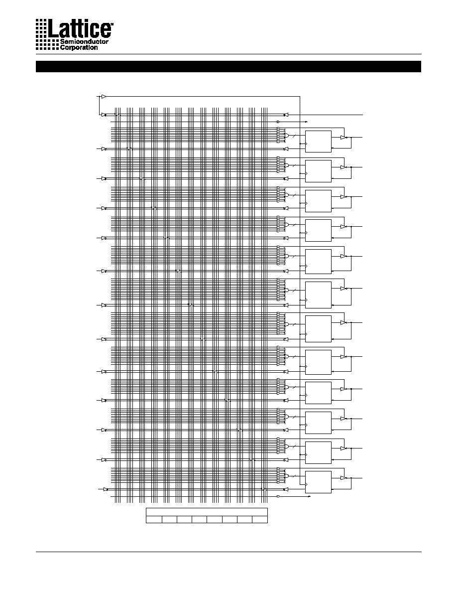
Functional Block Diagram
Pin Configuration

Specifications
GAL26CV12
2
)
s
n
(
d
p
T
)
s
n
(
u
s
T
)
s
n
(
o
c
T
)
A
m
(
c
c
I
#
g
n
i
r
e
d
r
O
e
g
a
k
c
a
P
5
.
7
6
5
.
4
0
3
1
P
L
7
-
C
2
1
V
C
6
2
L
A
G
P
I
D
c
i
t
s
a
l
P
n
i
P
-
8
2
0
3
1
J
L
7
-
C
2
1
V
C
6
2
L
A
G
C
C
L
P
d
a
e
L
-
8
2
0
1
7
7
0
3
1
P
L
0
1
-
B
2
1
V
C
6
2
L
A
G
P
I
D
c
i
t
s
a
l
P
n
i
P
-
8
2
0
3
1
J
L
0
1
-
B
2
1
V
C
6
2
L
A
G
C
C
L
P
d
a
e
L
-
8
2
5
1
0
1
8
0
3
1
P
L
5
1
-
B
2
1
V
C
6
2
L
A
G
P
I
D
c
i
t
s
a
l
P
n
i
P
-
8
2
0
3
1
J
L
5
1
-
B
2
1
V
C
6
2
L
A
G
C
C
L
P
d
a
e
L
-
8
2
0
2
2
1
2
1
0
3
1
P
L
0
2
-
B
2
1
V
C
6
2
L
A
G
P
I
D
c
i
t
s
a
l
P
n
i
P
-
8
2
0
3
1
J
L
0
2
-
B
2
1
V
C
6
2
L
A
G
C
C
L
P
d
a
e
L
-
8
2
)
s
n
(
d
p
T
)
s
n
(
u
s
T
)
s
n
(
o
c
T
)
A
m
(
c
c
I
#
g
n
i
r
e
d
r
O
e
g
a
k
c
a
P
0
1
7
7
0
5
1
I
P
L
0
1
-
C
2
1
V
C
6
2
L
A
G
P
I
D
c
i
t
s
a
l
P
n
i
P
-
8
2
0
5
1
I
J
L
0
1
-
C
2
1
V
C
6
2
L
A
G
C
C
L
P
d
a
e
L
-
8
2
5
1
0
1
8
0
5
1
I
P
L
5
1
-
B
2
1
V
C
6
2
L
A
G
P
I
D
c
i
t
s
a
l
P
n
i
P
-
8
2
0
5
1
I
J
L
5
1
-
B
2
1
V
C
6
2
L
A
G
C
C
L
P
d
a
e
L
-
8
2
0
2
2
1
2
1
0
5
1
I
P
L
0
2
-
B
2
1
V
C
6
2
L
A
G
P
I
D
c
i
t
s
a
l
P
n
i
P
-
8
2
0
5
1
I
J
L
0
2
-
B
2
1
V
C
6
2
L
A
G
C
C
L
P
d
a
e
L
-
8
2
Industrial Grade Specifications
Blank = Commercial
I = Industrial
Grade
Package
Power
L = Low Power
Speed (ns)
XXXXXXXX
XX
X
X X
Device Name
_
P = Plastic DIP
J = PLCC
GAL26CV12C
GAL26CV12B
GAL26CV12 Ordering Information
Commercial Grade Specifications
Part Number Description

Specifications
GAL26CV12
3
GAL26CV12 OUTPUT LOGIC MACROCELL (OLMC)
Each of the Macrocells of the GAL26CV12 has two primary
functional modes: registered, and combinatorial I/O. The modes
and the output polarity are set by two bits (SO and S1), which are
normally controlled by the logic compiler. Each of these two primary
modes, and the bit settings required to enable them, are described
below and on the the following page.
REGISTERED
In registered mode the output pin associated with an individual
OLMC is driven by the Q output of that OLMC's D-type flip-flop.
Logic polarity of the output signal at the pin may be selected by
specifying that the output buffer drive either true (active high) or
inverted (active low). Output tri-state control is available as an
individual product term for each OLMC, and can therefore be
defined by a logic equation. The D flip-flop's /Q output is fed back
into the AND array, with both the true and complement of the
feedback available as inputs to the AND array.
The GAL26CV12 has a product term for Asynchronous Reset (AR)
and a product term for Synchronous Preset (SP). These two prod-
uct terms are common to all registered OLMCs. The Asynchronous
Reset sets all registered outputs to zero any time this dedicated
product term is asserted. The Synchronous Preset sets all registers
to a logic one on the rising edge of the next clock pulse after this
product term is asserted.
NOTE: The AR and SP product terms will force the Q output of the
flip-flop into the same state regardless of the polarity of the output.
Therefore, a reset operation, which sets the register output to a zero,
may result in either a high or low at the output pin, depending on
the pin polarity chosen.
The GAL26CV12 has a variable number of product terms per
OLMC. Of the twelve available OLMCs, two OLMCs have access
to twelve product terms (pins 20 and 22), two have access to ten
product terms (pins 19 and 23), and the other eight OLMCs have
eight product terms each. In addition to the product terms available
for logic, each OLMC has an additional product term dedicated to
output enable control.
The output polarity of each OLMC can be individually programmed
to be true or inverting, in either combinatorial or registered mode.
This allows each output to be individually configured as either active
high or active low.
A R
S P
D
Q
Q
C L K
4 T O 1
M U X
2 T O 1
M U X
NOTE: In registered mode, the feedback is from the /Q output of
the register, and not from the pin; therefore, a pin defined as
registered is an output only, and cannot be used for dynamic
I/O, as can the combinatorial pins.
COMBINATORIAL I/O
In combinatorial mode the pin associated with an individual OLMC
is driven by the output of the sum term gate. Logic polarity of the
output signal at the pin may be selected by specifying that the output
buffer drive either true (active high) or inverted (active low). Output
tri-state control is available as an individual product term for each
output, and may be individually set by the compiler as either "on"
(dedicated output), "off" (dedicated input), or "product term driven"
(dynamic I/O). Feedback into the AND array is from the pin side of
the output enable buffer. Both polarities (true and inverted) of the
pin are fed back into the AND array.
Output Logic Macrocell (OLMC)
Output Logic Macrocell Configurations

Specifications
GAL26CV12
4
ACTIVE HIGH
ACTIVE LOW
ACTIVE HIGH
ACTIVE LOW
S
0
= 1
S
1
= 1
S
0
= 0
S
1
= 1
S
0
= 0
S
1
= 0
S
0
= 1
S
1
= 0
A R
S P
D
Q
Q
C L K
A R
S P
D
Q
Q
C L K
Registered Mode
Combinatorial Mode
Specifications
GAL26CV12
5
ASYNCHRONOUS RESET
(TO ALL REGISTERS)
0
4
8
12
16
20
24
28
32
36
40
44
48
1
0052
.
.
.
0468
2
27
28
OLMC
S0
6344
S1
6345
26
25
24
23
22
20
19
18
17
16
15
SYNCHRONOUS PRESET
(TO ALL REGISTERS)
14
13
12
11
10
OLMC
S0
6346
S1
6347
OLMC
S0
6348
S1
6349
OLMC
S0
6350
S1
6351
OLMC
S0
6352
S1
6353
OLMC
S0
6354
S1
6355
OLMC
S0
6356
S1
6357
OLMC
S0
6358
S1
6359
OLMC
S0
6360
S1
6361
OLMC
S0
6362
S1
6363
OLMC
S0
6364
S1
6365
OLMC
S0
6366
S1
6367
0000
0520
.
.
.
0936
0988
.
.
.
1404
1456
.
.
.
1872
1924
.
.
.
.
2444
3848
.
.
.
.
4368
2496
.
.
.
.
.
3120
3172
.
.
.
.
.
3796
4420
.
.
.
4836
4888
.
.
.
5304
5356
.
.
.
5772
5824
.
.
.
6240
6292
3
4
5
6
8
9
Electronic Signature
6368, 6369 ...
... 6430, 6431
L
S
B
M
S
B
Byte 7 Byte 6 Byte 5 Byte 4
Byte 2 Byte 1 Byte 0
Byte 3
8
8
8
8
10
12
12
10
8
8
8
8
GAL26CV12 Logic Diagram/JEDEC Fuse Map
DIP & PLCC Package Pinouts