GAL6002
High Performance E
2
CMOS FPLA
Generic Array LogicTM
1
ILMC
INPUT LOGIC MACROCELL
IOLMC I/O LOGIC MACROCELL
BLMC
BURIED LOGIC MACROCELL
OLMC
OUTPUT LOGIC MACROCELL
1
12
13
24
I/ICLK
I
I
I
I
I
I
I
I
I
I
GND
Vcc
I/O/Q
I/O/Q
I/O/Q
I/O/Q
I/O/Q
I/O/Q
I/O/Q
I/O/Q
OCLK
I/O/Q
I/O/Q
6
18
2
28
NC
I/ICLK
I
I
I
I
I
I
I
NC
NC
NC
GND
I
I
OCLK
I/O/Q
I/O/Q
I/O/Q
I/O/Q
I/O/Q
I/O/Q
I/O/Q
Vcc
I/O/Q
I
I/O/Q
I/O/Q
4
5
7
9
11
12
14
16
18
19
21
23
25
26
GAL6002
Top View
PLCC
DIP
GAL
6002
OUTPUT
ENABLE
AND
OR
D
11
2
INPUT
CLOCK
ICLK
14
23
IOLMC
ILMC
OLMC
E
RESET
OUTPUTS
14 - 23
14
23
0
7
BLMC
D
E
OUTPUT
CLOCK
OCLK
{
INPUTS
2-11
{
Copyright � 1997 Lattice Semiconductor Corp. All brand or product names are trademarks or registered trademarks of their respective holders. The specifications and information herein are subject
to change without notice.
LATTICE SEMICONDUCTOR CORP., 5555 Northeast Moore Ct., Hillsboro, Oregon 97124, U.S.A.
July 1997
Tel. (503) 268-8000; 1-800-LATTICE; FAX (503) 268-8556; http://www.latticesemi.com
6002_02
Features
� HIGH PERFORMANCE E
2
CMOS
�
TECHNOLOGY
-- 15ns Maximum Propagation Delay
-- 75MHz Maximum Frequency
-- 6.5ns Maximum Clock to Output Delay
-- TTL Compatible 16mA Outputs
-- UltraMOS
�
Advanced CMOS Technology
� ACTIVE PULL-UPS ON ALL PINS
� LOW POWER CMOS
-- 90mA Typical Icc
� E
2
CELL TECHNOLOGY
-- Reconfigurable Logic
-- Reprogrammable Cells
-- 100% Tested/100% Yields
-- High Speed Electrical Erasure (<100ms)
-- 20 Year Data Retention
� UNPRECEDENTED FUNCTIONAL DENSITY
-- 78 x 64 x 36 FPLA Architecture
-- 10 Output Logic Macrocells
-- 8 Buried Logic Macrocells
-- 20 Input and I/O Logic Macrocells
� HIGH-LEVEL DESIGN FLEXIBILITY
-- Asynchronous or Synchronous Clocking
-- Separate State Register and Input Clock Pins
-- Functional Superset of Existing 24-pin PAL
�
and FPLA Devices
� APPLICATIONS INCLUDE:
-- Sequencers
-- State Machine Control
-- Multiple PLD Device Integration
Description
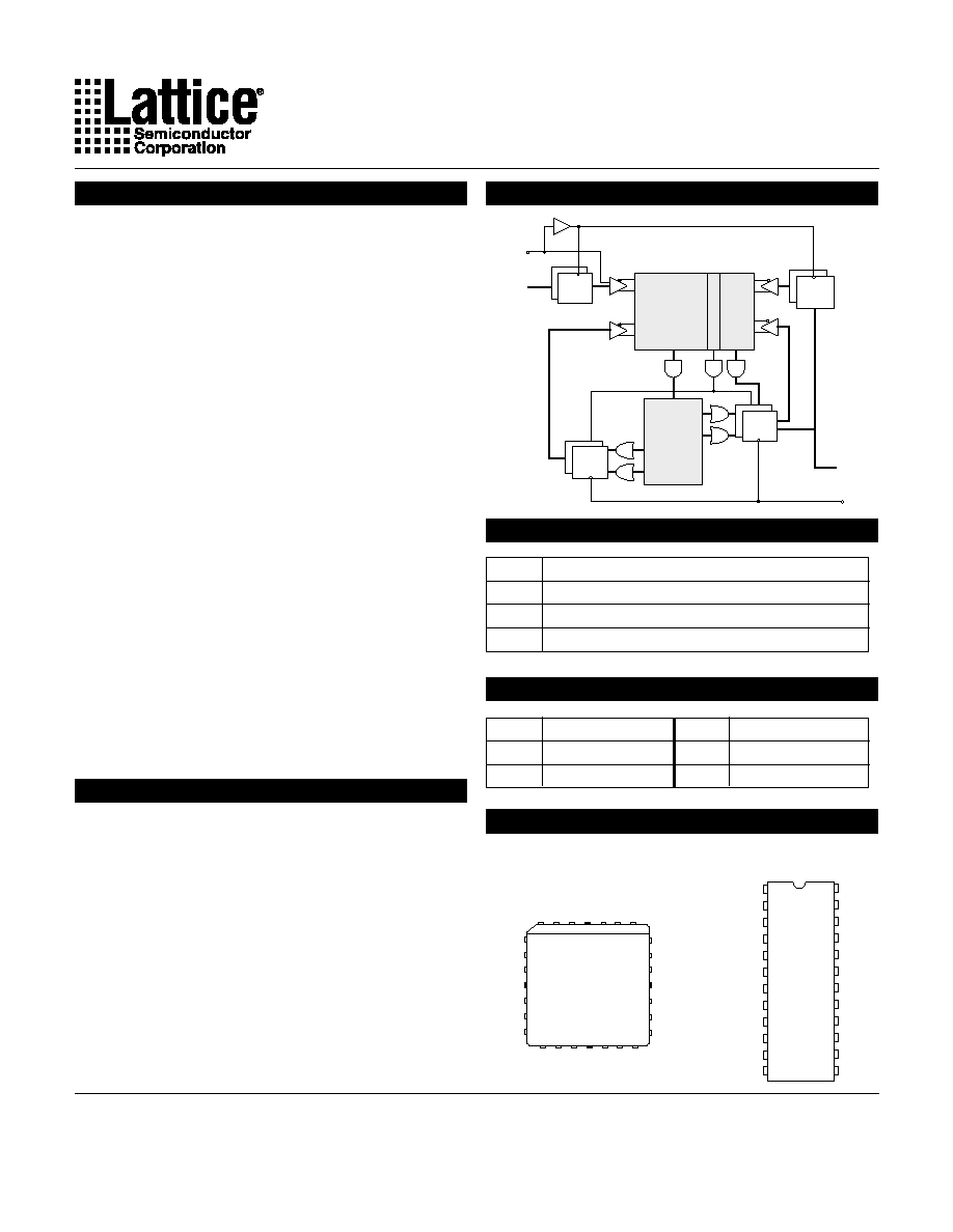
Having an FPLA architecture, the GAL6002 provides superior
flexibility in state-machine design. The GAL6002 offers the highest
degree of functional integration, flexibility, and speed currently
available in a 24-pin, 300-mil package. E
2
CMOS technology offers
high speed (<100ms) erase times, providing the ability to reprogram
or reconfigure the device quickly and efficiently.
The GAL6002 has 10 programmable Output Logic Macrocells
(OLMC) and 8 programmable Buried Logic Macrocells (BLMC). In
addition, there are 10 Input Logic Macrocells (ILMC) and 10
I/O Logic Macrocells (IOLMC). Two clock inputs are provided for
independent control of the input and output macrocells.
Unique test circuitry and reprogrammable cells allow complete AC,
DC, and functional testing during manufacturing. As a result, Lattice
Semiconductor delivers 100% field programmability and
functionality of all GAL products. In addition, 100 erase/write cycles
and data retention in excess of 20 years are specified.
Pin Configuration
Macrocell Names
PinNames
I
0
- I
10
INPUT
I/O/Q
BIDIRECTIONAL
ICLK
INPUT CLOCK
V
CC
POWER (+5V)
OCLK
OUTPUT CLOCK
GND
GROUND
Functional Block Diagram

Specifications
GAL6002
2
Blank = Commercial
Grade
Package
Power
L = Low Power
Speed (ns)
XXXXXXXX
XX
X
X X
Device Name
_
P = Plastic DIP
J = PLCC
GAL6002B
)
s
n
(
d
p
T
)
z
H
M
(
x
a
m
F
)
A
m
(
c
c
I
#
g
n
i
r
e
d
r
O
e
g
a
k
c
a
P
5
1
5
7
5
3
1
P
L
5
1
-
B
2
0
0
6
L
A
G
P
I
D
c
i
t
s
a
l
P
n
i
P
-
4
2
5
3
1
J
L
5
1
-
B
2
0
0
6
L
A
G
C
C
L
P
d
a
e
L
-
8
2
0
2
0
6
5
3
1
P
L
0
2
-
B
2
0
0
6
L
A
G
P
I
D
c
i
t
s
a
l
P
n
i
P
-
4
2
5
3
1
J
L
0
2
-
B
2
0
0
6
L
A
G
C
C
L
P
d
a
e
L
-
8
2
GAL6002 Commercial Device Ordering Information
Commercial Grade Specifications
Part Number Description
Specifications
GAL6002
3
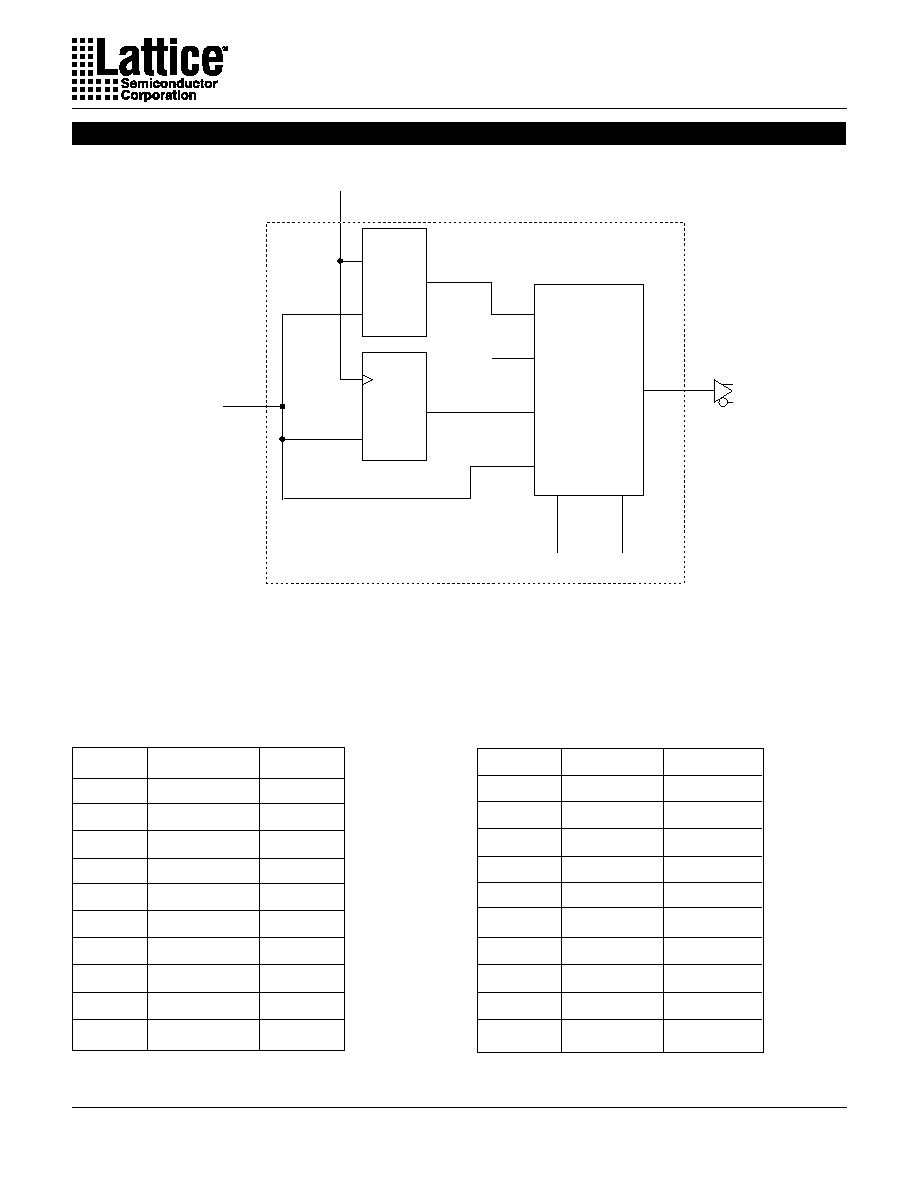
The GAL6002 features two configurable input sections. The ILMC
section corresponds to the dedicated input pins (2-11) and the
IOLMC to the I/O pins (14-23). Each input section is individually
configurable as asynchronous, latched, or registered inputs. Pin
1 (ICLK) is used as an enable input for latched macrocells or as a
clock input for registered macrocells. Individually configurable
inputs provide system designers with unparalleled design flexibility.
With the GAL6002, external input registers and latches are not
necessary.
Both the ILMC and the IOLMC are individually configurable and the
ILMC can be configured independently of the IOLMC. The three
valid macrocell configurations and its associated fuse numbers are
shown in the diagrams on the following pages. Note that these
programmable cells are configured by the logic compiler software.
The user does not need to manually manipulate these architecture
bits.
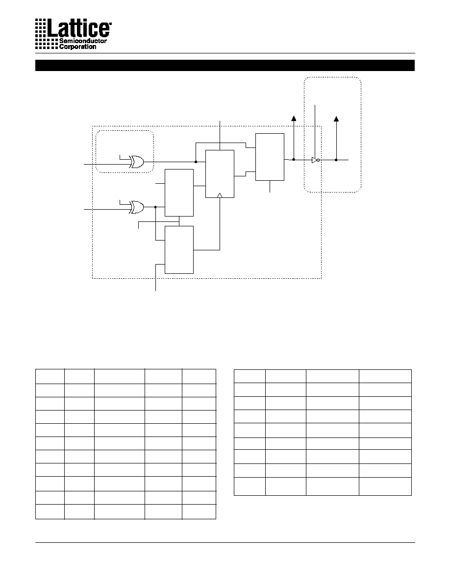
The outputs of the OR array feed two groups of macrocells. One
group of eight macrocells is buried; its outputs feed back directly
into the AND array rather than to device pins. These cells are called
the Buried Logic Macrocells (BLMC), and are useful for building
state machines. The second group of macrocells consists of 10
cells whose outputs, in addition to feeding back into the AND array,
are available at the device pins. Cells in this group are known as
Output Logic Macrocells (OLMC).
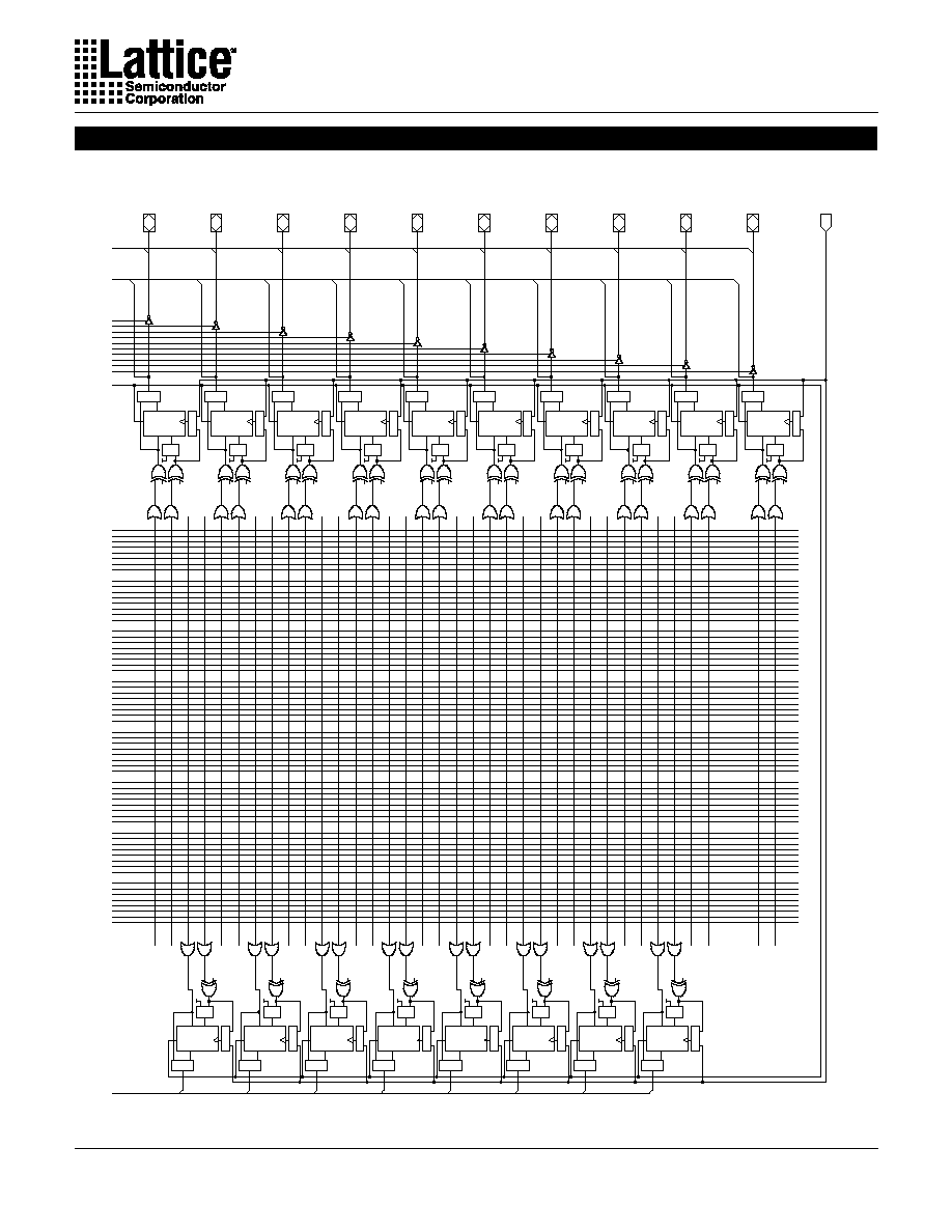
The Output and Buried Logic Macrocells are configurable on a
macrocell by macrocell basis. Buried and Output Logic Macrocells
may be set to one of three configurations: combinational, D-type
register with sum term (asynchronous) clock, or D/E-type register.
Output macrocells always have I/O capability, with directional control
provided by the 10 output enable (OE) product terms. Additionally,
the polarity of each OLMC output is selected through the
programmable polarity control cell called XORD. Polarity selection
for BLMCs is selected through the true and complement forms of
their feedbacks to the AND array. Polarity of all E (Enable) sum
terms is selected through the XORE programmable cells.
When the output or buried logic macrocell is configured as a
D/E type register, the register is clocked from the common OCLK
and the register clock enable input is controlled by the associated
"E" sum term. This configuration is useful for building counters and
state-machines with count hold and state hold functions.
When the macrocell is configured as a D type register with a sum
term clock, the register is always enabled and the associated "E"
sum term is routed directly to the clock input. This permits
asynchronous programmable clocking, selected on a register-by-
register basis.
Registers in both the Output and Buried Logic Macrocells feature
a common RESET product term. This active high product term
allows the registers to be asynchronously reset. All registers reset
to logic zero. With the inverting output buffers, the output pins will
reset to logic one.
There are two possible feedback paths from each OLMC. The first
path is directly from the OLMC (this feedback is before the output
buffer). When the OLMC is used as an output, the second feedback
path is through the IOLMC. With this dual feedback arrangement,
the OLMC can be permanently buried without losing the use of the
associated OLMC pin as an input, or dynamically buried with the
use of the output enable product term.
The D/E registers used in this device offer the designer the ultimate
in flexibility and utility. The D/E register architecture can emulate
RS, JK, and T registers with the same efficiency as a dedicated RS,
JK, or T registers.
The three macrocell configurations are shown in the diagrams on
the following pages. These programmable cells are also configured
by the logic compiler software. The user does not need to manually
manipulate these architecture bits.
Input Logic Macrocell (ILMC) and I/O Logic Macrocell (IOLMC)
Output Logic Macrocell (OLMC) and Buried Logic Macrocell (BLMC)
Specifications
GAL6002
4
Input Macrocell JEDEC Fuse Numbers
INSYNC
INLATCH
ILMC
8218
8219
0
8220
8221
1
8222
8223
2
8224
8225
3
8226
8227
4
8228
8229
5
8230
8231
6
8232
8233
7
8234
8235
8
8236
8237
9
I/O Macrocell JEDEC Fuse Numbers
IOSYNC
IOLATCH
IOLMC
8238
8239
9
8240
8241
8
8242
8243
7
8244
8245
6
8246
8247
5
8248
8249
4
8250
8251
3
8252
8253
2
8254
8255
1
8256
8257
0
MUX
INVALID
LATCH
REG.
D
Q
E
D
Q
ICLK
0 0
0 1
1 0
1 1
ISYN(i)
AND
ARRAY
LATCH(i)
INPUT
or I/O
ILMC/IOLMC
Generic Logic Block Diagram
ILMC and IOLMC Configurations
Specifications
GAL6002
5
OLMC/BLMC
Generic Logic Block Diagram
OLMC JEDEC Fuse Numbers
OLMC
CKS
OUTSYNC
XORE
XORD
0
8178
8179
8180
8181
1
8182
8183
8184
8185
2
8186
8187
8188
8189
3
8190
8191
8192
8193
4
8194
8195
8196
8197
5
8198
8199
8200
8201
6
8202
8203
8204
8205
7
8206
8207
8208
8209
8
8210
8211
8212
8213
9
8214
8215
8216
8217
BLMC JEDEC Fuse Numbers
BLMC
CKS
OUTSYNC
XORE
7
8175
8176
8177
6
8172
8173
8174
5
8169
8170
8171
4
8166
8167
8168
3
8163
8164
8165
2
8160
8161
8162
1
8157
8158
8159
0
8154
8155
8156
D
Q
E
OSYN(i)
MUX
0
1
R
MUX
0
1
CKS(i)
Vcc
MUX
0
1
RESET
IOLMC
I/O
AND
ARRAY
OE
PRODUCT
TERM
OCLK
D
E
OLMC ONLY
OLMC ONLY
XORD(i)
XORE(i)
OLMC and BLMC Configurations
Specifications
GAL6002
6
IO
L
M
C
9
IO
L
M
C
8
IO
L
M
C
7
IO
L
M
C
6
IO
L
M
C
5
IO
L
M
C
4
IO
L
M
C
3
IO
L
M
C
2
IO
L
M
C
1
IO
L
M
C
0
OL
MC 0
OL
M
C
1
OL
MC 2
OL
M
C
3
OL
MC 4
OL
MC
5
OL
MC 6
OL
MC
7
OL
MC 8
OL
M
C
9
ICLK
IL
M
C
0
IL
M
C
1
IL
M
C
2
IL
M
C
3
IL
M
C
4
IL
M
C
5
IL
M
C
6
IL
M
C
7
IL
M
C
8
IL
M
C
9
BL
M
C
0
BL
M
C
7
BL
M
C
6
BL
M
C
5
BL
M
C
4
BL
M
C
1
BL
M
C
2
BL
M
C
3
1(
2
)
2(
3)
3(
4
)
4(
5)
5(
6)
6(
7)
7(
9
)
8(
1
0
)
9(
1
1
)
10(
1
2)
11
(
1
3)
Logic Diagram
Specifications
GAL6002
7
XO
RD
XO
RE
0
1
D
E
R
Q
01
1
0
XO
RD
XO
RE
0
1
D
E
R
Q
01
1
0
XO
RD
XO
RE
0
1
D
E
R
Q
01
1
0
XO
RD
XO
RE
0
1
D
E
R
Q
01
1
0
XO
RD
XO
RE
0
1
D
E
R
Q
01
1
0
XO
RD
XO
RE
0
1
D
E
R
Q
01
1
0
XO
R
D
XO
R
E
0
1
D
E
R
Q
01
1
0
XO
R
D
XO
R
E
0
1
D
E
R
Q
01
1
0
XO
R
D
XO
R
E
0
1
D
E
R
Q
01
1
0
XO
RD
XO
RE
0
1
D
E
R
Q
01
1
0
XO
R
E
0
1
D
E
R
Q
0
1
1
0
XO
R
E
0
1
D
E
R
Q
0
1
1
0
XO
RE
0
1
D
E
R
Q
0
1
1
0
XO
RE
0
1
D
E
R
Q
0
1
1
0
XO
RE
0
1
D
E
R
Q
0
1
1
0
XO
RE
0
1
D
E
R
Q
0
1
1
0
XO
RE
0
1
D
E
R
Q
0
1
1
0
XO
RE
0
1
D
E
R
Q
0
1
1
0
23
(
2
7
)
13(
1
6)
14
(
1
7)
15
(
1
8)
16(
19)
17(
20)
18(
21)
19(
23)
20(
2
4)
21(
2
5)
22
(
2
6)
BL
M
C
0
BL
M
C
1
BL
M
C
2
BL
M
C
3
BL
M
C
4
BL
M
C
5
BL
M
C
6
BL
M
C
7
OL
M
C
9
OL
M
C
8
OL
M
C
7
OL
M
C
6
OL
M
C
5
OL
M
C
4
OL
M
C
3
OL
M
C
2
OL
M
C
1
OL
M
C
0
R
ESET
OC
L
K
Logic Diagram (Continued)

Specifications
GAL6002
8
Recommended Operating Conditions
Commercial Devices:
Ambient Temperature (T
A
) ............................... 0 to 75
�
C
Supply voltage (V
CC
)
with Respect to Ground ..................... +4.75 to +5.25V
Absolute Maximum Ratings
(1)
Supply voltage V
CC
...................................... �0.5 to +7V
Input voltage applied .......................... �2.5 to V
CC
+1.0V
Off-state output voltage applied ......... �2.5 to V
CC
+1.0V
Storage Temperature ................................ �65 to 150
�
C
Ambient Temperature with
Power Applied ........................................ �55 to 125
�
C
1.Stresses above those listed under the "Absolute Maximum
Ratings" may cause permanent damage to the device. These
are stress only ratings and functional operation of the device at
these or at any other conditions above those indicated in the
operational sections of this specification is not implied (while
programming, follow the programming specifications).
COMMERCIAL
I
CC
Operating Power
V
IL
= 0.5V V
IH
= 3.0V
L -15/-20
--
90
135
mA
Supply Current
f
toggle
= 15MHz Outputs Open
V
IL
Input Low Voltage
Vss � 0.5
--
0.8
V
V
IH
Input High Voltage
2.0
--
Vcc+1
V
I
IL
1
Input or I/O Low Leakage Current
0V
V
IN
V
IL
(MAX.)
--
--
-100
�
A
I
IH
Input or I/O High Leakage Current
3.5V
V
IN
V
CC
--
--
10
�
A
V
OL
Output Low Voltage
I
OL
= MAX. Vin = V
IL
or V
IH
--
--
0.5
V
V
OH
Output High Voltage
I
OH
= MAX. Vin = V
IL
or V
IH
2.4
--
--
V
I
OL
Low Level Output Current
--
--
16
mA
I
OH
High Level Output Current
--
--
�3.2
mA
I
OS
2
Output Short Circuit Current
V
CC
= 5V
V
OUT
= 0.5V T
A
= 25
�
C
�30
--
�130
mA
SYMBOL
PARAMETER
CONDITION
MIN.
TYP.
3
MAX.
UNITS
1) The leakage current is due to the internal pull-up resistor on all pins. See Input Buffer section for more information.
2) One output at a time for a maximum duration of one second. Vout = 0.5V was selected to avoid test problems caused by tester
ground degradation. Characterized but not 100% tested.
3) Typical values are at Vcc = 5V and T
A
= 25
�
C
SYMBOL
PARAMETER
MAXIMUM*
UNITS
TEST CONDITIONS
C
I
Input Capacitance
8
pF
V
CC
= 5.0V, V
I
= 2.0V
C
I/O
I/O Capacitance
8
pF
V
CC
= 5.0V, V
I/O
= 2.0V
*Characterized but not 100% tested.
DC Electrical Characteristics
Over Recommended Operating Conditions (Unless Otherwise Specified)
Capacitance (TA = 25
�
C, f = 1.0 MHz)

Specifications
GAL6002
9
AC Switching Characteristics
Over Recommended Operating Conditions
t
pd1
A
Combinatorial Input to Combinatorial Output
--
15
--
20
ns
t
pd2
A
Feedback or I/O to Combinational Output
--
15
--
20
ns
t
pd3
A
Transparent Latch Input to Combinatorial Output
--
18
--
23
ns
t
co1
A
Input Latch ICLK to Combinatorial Output Delay
--
20
--
25
ns
t
co2
A
Input Reg. ICLK to Combinatorial Output Delay
--
20
--
25
ns
t
co3
A
Output D/E Reg. OCLK to Output Delay
--
6.5
--
8
ns
t
co4
A
Output D Reg. Sum Term CLK to Output Delay
--
18
--
20
ns
t
cf1
2
--
Output D/E Reg. OCLK to Buried Feedback Delay
--
3.6
--
7
ns
t
cf2
2
--
Output D Reg. STCLK to Buried Feedback Delay
--
10.1
--
13
ns
t
su1
--
Setup Time, Input before Input Latch ICLK
1.5
--
2
--
ns
t
su2
--
Setup Time, Input before Input Reg. ICLK
1.5
--
2
--
ns
t
su3
--
Setup Time, Input or Fdbk before D/E Reg. OCLK
11.5
--
13
--
ns
t
su4
--
Setup Time, Input or Fdbk before D Reg. Sum Term CLK
5
--
7
--
ns
t
su5
--
Setup Time, Input Reg. ICLK before D/E Reg. OCLK
15
--
20
--
ns
t
su6
--
Setup Time, Input Reg. ICLK before D Reg. Sum Term CLK
7
--
9
--
ns
t
h1
--
Hold Time, Input after Input Latch ICLK
3
--
4
--
ns
t
h2
--
Hold Time, Input after Input Reg. ICLK
3
--
4
--
ns
t
h3
--
Hold Time, Input or Feedback after D/E Reg. OCLK
0
--
0
--
ns
t
h4
--
Hold Time, Input or Feedback after D Reg. Sum Term CLK
4
--
6
--
ns
f
max1
3
--
Max. Clock Frequency w/External Feedback, 1/(
t
su3+
t
co3)
55.5 --
47.6 --
MHz
f
max2
3
--
Max. Clock Frequency w/External Feedback, 1/(
t
su4+
t
co4)
43.4 --
37
--
MHz
f
max3
3
--
Max. Clock Frequency w/Internal Feedback, 1/(
t
su3+
t
cf1)
66
--
50
--
MHz
f
max4
3
--
Max. Clock Frequency w/Internal Feedback, 1/(
t
su4+
t
cf2)
66
--
50
--
MHz
f
max5
3
--
Max. Clock Frequency w/No Feedback, OCLK
75
--
60
--
MHz
f
max6
3
--
Max. Clock Frequency w/No Feedback, STCLK
70
--
60
--
MHz
t
wh1
--
ICLK Pulse Duration, High
6
--
7
--
ns
t
wh2
--
OCLK Pulse Duration, High
6
--
7
--
ns
t
wh3
--
STCLK Pulse Duration, High
7
--
8
--
ns
UNITS
1) Refer to Switching Test Conditions section.
2) Calculated from fmax with internal feedback. Refer to fmax Description section.
3) Refer to fmax Description section.
PARAM.
TEST
COND
1
.
DESCRIPTION
-20
MIN. MAX.
-15
MIN. MAX.
COM
COM
Specifications
GAL6002
10
UNITS
PARAMETER
TEST
COND
1
.
DESCRIPTION
t
wl1
--
ICLK Pulse Duration, Low
6
--
7
--
ns
t
wl2
--
OCLK Pulse Duration, Low
6
--
7
--
ns
t
wl3
--
STCLK Pulse Duration, Low
7
--
8
--
ns
t
arw
--
Reset Pulse Duration
12
--
15
--
ns
t
en
B
Input or I/O to Output Enabled
--
15
--
20
ns
t
dis
C
Input or I/O to Output Disabled
--
15
--
20
ns
t
ar
A
Input or I/O to Asynchronous Reg. Reset
--
16
--
20
ns
t
arr1
--
Asynchronous Reset to OCLK Recovery Time
11
--
14
--
ns
t
arr2
--
Asynchronous Reset to Sum Term CLK Recovery Time
4
--
6
--
ns
1) Refer to Switching Test Conditions section.
-20
MIN. MAX.
-15
MIN. MAX.
COM
COM
AC Switching Characteristics (Continued)
Over Recommended Operating Conditions

Specifications
GAL6002
11
Asynchronous Reset
REGISTERED
OUTPUT
t
arw
t
ar
INPUT or
I/O FEEDBACK
DRIVING AR
OCLK
Sum Term CLK
t
arr2
t
arr1
VALID INPUT
COMBINATORIAL
OUTPUT
t
pd1,2
INPUT or
I/O FEEDBACK
Combinatorial Output
Latched Input
INPUT or
I/O FEEDBACK
VALID INPUT
COMBINATORIAL
OUTPUT
ICLK (LATCH)
t
su1
t
h1
t
co1
t
pd3
INPUT or
I/O FEEDBACK
VALID INPUT
REGISTERED
OUTPUT
Sum Term CLK
t
su4
t
h4
t
co4
1/
f
max2
Input or I/O to Output Enable/Disable
Clock Width
ICLK or
OCLK
Sum Term CLK
t
wh1,2
t
wl1,2
t
wl3
t
wh3
Registered Output (Sum Term CLK)
Registered Output (OCLK)
INPUT or
I/O FEEDBACK
VALID INPUT
REGISTERED
OUTPUT
OCLK
1/
f
max1
t
su3
t
h3
t
co3
Registered Input
INPUT or
I/O FEEDBACK
VALID INPUT
COMBINATORIAL
OUTPUT
ICLK (REGISTER)
OCLK
Sum Term CLK
t
su2
t
h2
t
co2
t
su5
t
su6
t
en
t
dis
INPUT or
I/O FEEDBACK
OUTPUT
Switching Waveforms
Specifications
GAL6002
12
f
max with External Feedback 1/(
t
su+
t
co)
Note: fmax with external feedback is calculated from measured
tsu and tco.
f
max with Internal Feedback 1/(
t
su+
t
cf)
Note: tcf is a calculated value, derived by subtracting tsu from
the period of fmax w/internal feedback (tcf = 1/fmax - tsu). The
value of tcf is used primarily when calculating the delay from
clocking a register to a combinatorial output (through registered
feedback), as shown above. For example, the timing from clock
to a combinatorial output is equal to tcf + tpd.
f
max with No Feedback
Note: fmax with no feedback may be less than 1/(twh + twl). This
is to allow for a clock duty cycle of other than 50%.
Input Pulse Levels
GND to 3.0V
Input Rise and Fall Times
3ns 10% � 90%
Input Timing Reference Levels
1.5V
Output Timing Reference Levels
1.5V
Output Load
See Figure
3-state levels are measured 0.5V from steady-state active
level.
Test Condition
R
1
R
2
C
L
A
300
390
50pF
B
Active High
390
50pF
Active Low
300
390
50pF
C
Active High
390
5pF
Active Low
300
390
5pF
TEST POINT
C *
L
FROM OUTPUT (O/Q)
UNDER TEST
+5V
*C
L
INCLUDES TEST FIXTURE AND PROBE CAPACITANCE
R
2
R
1
REGISTER
LOGIC
ARRAY
t
co
t
su
CLK
REGISTER
LOGIC
ARRAY
CLK
CLK
REGISTER
LOGIC
ARRAY
t
cf
t
pd
fmax Descriptions
Switching Test Conditions
Output Load Conditions (see figure)
Specifications
GAL6002
13
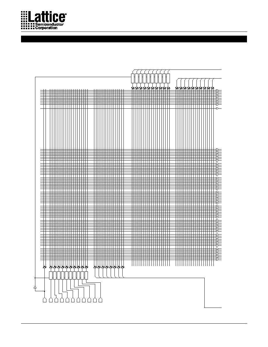
Array Description
The GAL6002 contains two E
2
reprogrammable arrays. The first is
an AND array and the second is an OR array. These arrays are de-
scribed in detail below.
AND ARRAY
The AND array is organized as 78 inputs by 75 product term outputs.
The 10 ILMCs, 10 IOLMCs, 8 BLMC feedbacks, 10 OLMC feed-
backs, and ICLK comprise the 39 inputs to this array (each available
in true and complement forms). 64 product terms serve as inputs
to the OR array. The RESET product term generates the RESET
signal described in the Output and Buried Logic Macrocells sec-
tion. There are 10 output enable product terms which allow device
I/O pins to be bi-directional or tri-state.
OR ARRAY
The OR array is organized as 64 inputs by 36 sum term outputs.
64 product terms from the AND array serve as the inputs to the OR
array. Of the 36 sum term outputs, 18 are data ("D") terms and 18
are enable/clock ("E") terms. These terms feed into the 10 OLMCs
and 8 BLMCs, one "D" term and one "E" term to each.
The programmable OR array offers unparalleled versatility in prod-
uct term usage. This programmability allows from 1 to 64 product
terms to be connected to a single sum term. A programmable OR
array is more flexible than a fixed, shared, or variable product term
architecture.
Electronic Signature
An electronic signature is provided with every GAL6002 device. It
contains 72 bits of reprogrammable memory that can contain user
defined data. Some uses include user ID codes, revision numbers,
or inventory control. The signature data is always available to the
user independent of the state of the security cell.
NOTE: The electronic signature is included in checksum calcula-
tions. Changing the electronic signature will alter the checksum.
Security Cell
A security cell is provided with every GAL6002 device as a deterrent
to unauthorized copying of the array patterns. Once programmed,
this cell prevents further read access to the AND array. This cell
can be erased only during a bulk erase cycle, so the original con-
figuration can never be examined once this cell is programmed.
The Electronic Signature is always available to the user, regard-
less of the state of this control cell.
Device Programming
GAL devices are programmed using a Lattice Semiconductor-
approved Logic Programmer, available from a number of manufac-
turers. Complete programming of the device takes only a few
seconds. Erasing of the device is transparent to the user, and is
done automatically as part of the programming cycle.
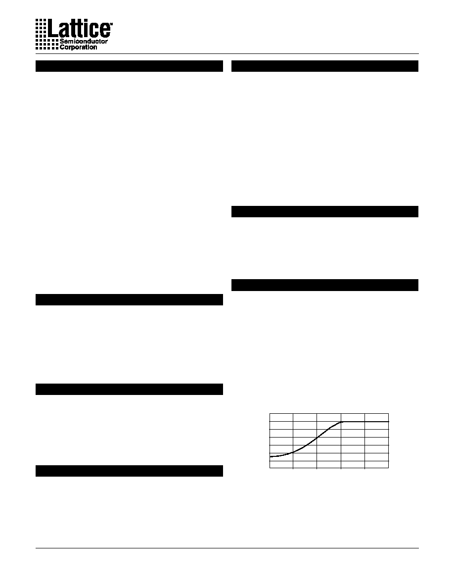
Typical Input Pull-up Characteristic
1 . 0
2 . 0
3 . 0
4 . 0
5 . 0
- 6 0
0
- 2 0
- 4 0
0
In p u t V o lt ag e ( V o lt s)
I
nput
C
u
r
r
e
nt
(
u
A
)
Register Preload
When testing state machine designs, all possible states and state
transitions must be verified, not just those required during normal
operations. This is because certain events may occur during sys-
tem operation that cause the logic to be in an illegal state (power-
up, line voltage glitches, brown-out, etc.). To test a design for proper
treatment of these conditions, a method must be provided to break
the feedback paths and force any desired state (i.e., illegal) into the
registers. Then the machine can be sequenced and the outputs
tested for correct next state generation.
All of the registers in the GAL6002 can be preloaded, including the
ILMC, IOLMC, OLMC, and BLMC registers. In addition, the con-
tents of the state and output registers can be examined in a special
diagnostics mode. Programming hardware takes care of all preload
timing and voltage requirements.
Latch-Up Protection
GAL6002 devices are designed with an on-board charge pump to
negatively bias the substrate. The negative bias is of sufficient
magnitude to prevent input undershoots from causing the circuitry
to latch. Additionally, outputs are designed with n-channel pull-ups
instead of the traditional p-channel pull-ups to eliminate any pos-
sibility of SCR induced latching.
Input Buffers
GAL6002 devices are designed with TTL level compatible input
buffers. These buffers have a characteristically high impedance,
and present a much lighter load to the driving logic than bipolar TTL
devices.
GAL6002 input buffers have active pull-ups within their input struc-
ture. This pull-up will cause any un-terminated input or I/O to float
to a TTL high (logical 1). Lattice Semiconductor recommends that
all unused inputs and tri-stated I/O pins be connected to another
active input, Vcc, or GND. Doing this will tend to improve noise
immunity and reduce Icc for the device.

Specifications
GAL6002
14
Vcc
CLK
INTERNAL REGISTER
Q - OUTPUT
FEEDBACK/EXTERNAL
OUTPUT REGISTER
Vcc (min.)
t
pr
Internal Register
Reset to Logic "0"
Device Pin
Reset to Logic "1"
t
wl
t
su
Circuitry within the GAL6002 provides a reset signal to all registers
during power-up. All internal registers will have their Q outputs
set low after a specified time (tpr, 1
�
s MAX). As a result, the state
on the registered output pins (if they are enabled) will always be
high on power-up, regardless of the programmed polarity of the
output pins. This feature can greatly simplify state machine design
by providing a known state on power-up. The timing diagram for
power-up is shown below. Because of the asynchronous nature
of system power-up, some conditions must be met to provide a
valid power-up reset of the GAL6002. First, the V
CC
rise must be
monotonic. Second, the clock input must be at static TTL level
as shown in the diagram during power up. The registers will reset
within a maximum of tpr time. As in normal system operation,
avoid clocking the device until all input and feedback path setup
times have been met. The clock must also meet the minimum
pulse width requirements.
The number of Differential Product Term Switching (DPTS ) for
a given design is calculated by subtracting the total number of
product terms that are switching from a Logical HI to a Logical LO
from those switching from a Logical LO to a Logical HI within a
5ns period. After subtracting take the absolute value.
DPTS =
(P-Terms)
LH
- (P-Terms)
HL
DPTS restricts the number of product terms that can be switched
simultaneously - there is no limit on the number of product terms
that can be used.
The majority of designs fall below 15 DPTS, with the upper limit
being approximately 25 DPTS. Lattice Semiconductor guarantees
and tests the commercial grade GAL6002 for functionality at
DPTS
30.
A software utility is available from Lattice Semiconductor
Applications Engineering that will perform this calculation on any
GAL6002 JEDEC file. This program, DPTS, and additional
information may be obtained from your local Lattice
Semiconductor representative or by contacting Lattice
Semiconductor Applications Engineering Dept. (Tel: 503-681-0118
or 1-888-ISP-PLDS; FAX: 681-3037).
Power-Up Reset
Differential Product Term Switching (DPTS) Applications
Specifications
GAL6002
15
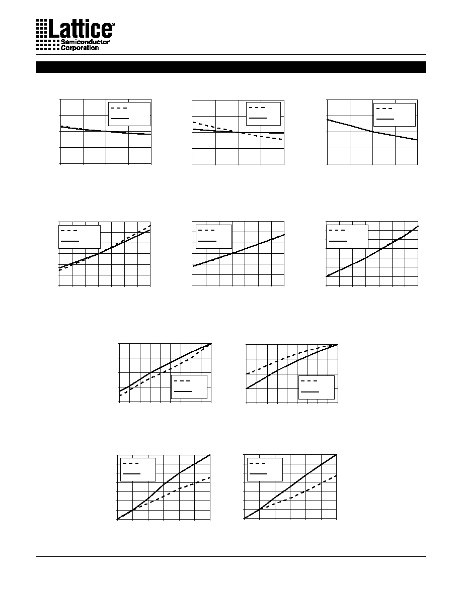
Normalized Tpd vs Vcc
Supply Voltage (V)
Normalized Tpd
0.8
0.9
1
1.1
1.2
4.50
4.75
5.00
5.25
5.50
PT H->L
PT L->H
Normalized Tco vs Vcc
Supply Voltage (V)
Normalized Tco
0.8
0.9
1
1.1
1.2
4.50
4.75
5.00
5.25
5.50
RISE
FALL
Normalized Tsu vs Vcc
Supply Voltage (V)
Normalized Tsu
0.8
0.9
1
1.1
1.2
4.50
4.75
5.00
5.25
5.50
PT H->L
PT L->H
Normalized Tpd vs Temp
Temperature (deg. C)
Normalized Tpd
0.7
0.8
0.9
1
1.1
1.2
1.3
-55
-25
0
25
50
75
100
125
PT H->L
PT L->H
Normalized Tco vs Temp
Temperature (deg. C)
Normalized Tco
0.7
0.8
0.9
1
1.1
1.2
1.3
-55
-25
0
25
50
75
100
125
RISE
FALL
Normalized Tsu vs Temp
Temperature (deg. C)
Normalized Tsu
0.7
0.8
0.9
1
1.1
1.2
1.3
1.4
-55
-25
0
25
50
75
100
125
PT H->L
PT L->H
Delta Tpd vs # of Outputs
Switching
Number of Outputs Switching
Delta Tpd (ns)
-2
-1.5
-1
-0.5
0
1
2
3
4
5
6
7
8
9
10
RISE
FALL
Delta Tco vs # of Outputs
Switching
Number of Outputs Switching
Delta Tco (ns)
-2
-1.5
-1
-0.5
0
1
2
3
4
5
6
7
8
9
10
RISE
FALL
Delta Tpd vs Output Loading
Output Loading (pF)
Delta Tpd (ns)
-2
0
2
4
6
8
10
12
0
50
100
150
200
250
300
RISE
FALL
Delta Tco vs Output Loading
Output Loading (pF)
Delta Tco (ns)
-2
0
2
4
6
8
10
12
0
50
100
150
200
250
300
RISE
FALL
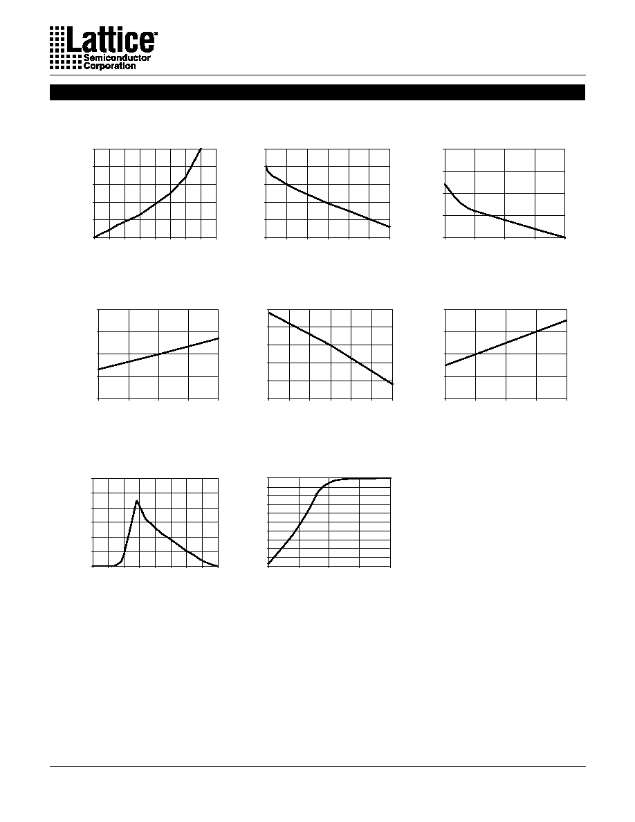
Typical AC and DC Characteristic Diagrams
Specifications
GAL6002
16
Vol vs Iol
Iol (mA)
Vol (V)
0
0.5
1
1.5
2
2.5
0.00
20.00
40.00
60.00
80.00
Voh vs Ioh
Ioh(mA)
Voh (V)
0
1
2
3
4
5
0.00
10.00
20.00
30.00
40.00
50.00
60.00
Voh vs Ioh
Ioh(mA)
Voh (V)
3.5
3.75
4
4.25
4.5
0.00
1.00
2.00
3.00
4.00
Normalized Icc vs Vcc
Supply Voltage (V)
Normalized Icc
0.80
0.90
1.00
1.10
1.20
4.50
4.75
5.00
5.25
5.50
Normalized Icc vs Temp
Temperature (deg. C)
Normalized Icc
0.7
0.8
0.9
1
1.1
1.2
-55
-25
0
25
75
100
125
Normalized Icc vs Freq.
Frequency (MHz)
Normalized Icc
0.80
0.90
1.00
1.10
1.20
0
25
50
75
100
Delta Icc vs Vin (1 input)
Vin (V)
Delta Icc (mA)
0
0.5
1
1.5
2
2.5
3
0.00 0.50 1.00 1.50 2.00 2.50 3.00 3.50 4.00
Input Clamp (Vik)
Vik (V)
Iik (mA)
0
10
20
30
40
50
60
70
80
90
100
-2.00
-1.50
-1.00
-0.50
0.00
Typical AC and DC Characteristic Diagrams