World's
Fastest &
Smallest
SPLD
www.latticesemi.com
1
isp22av_01
ispGAL22V10AV/B/C
In-System Programmable Low Voltage
E
2
CMOS
PLD Generic Array Logic
February 2003
Preliminary Data Sheet
��
� 2003 Lattice Semiconductor Corp. All Lattice trademarks, registered trademarks, patents, and disclaimers are as listed at www.latticesemi.com/legal. All other
brand or product names are trademarks or registered trademarks of their respective holders. The specifications and information herein are subject to change without
notice.
Features
High Performance
� t
PD
= 2.3ns propagation delay
� f
MAX
= 455 MHz maximum operating frequency
� t
CO
= 2ns maximum from clock input to data
output
� t
SU
= 1.3 ns clock set-up time
Low Power
� 1.8V core E
2
CMOS
�
technology
� Typical standby power <300�W
(ispGAL22V10AC)
� CMOS design techniques provide low static and
dynamic power
Space-Saving Packaging
� Available in 32-pin QFN (Quad Flat-pack No
lead), 5mm x 5mm body size
Easy System Integration
� Operation with 3.3V (ispGAL22V10AV), 2.5V
(ispGAL22V10AB) or 1.8V (ispGAL22V10AC)
supplies
� Operation with 3.3V, 2.5V or 1.8V LVCMOS I/O
� 5V tolerant I/O for LVCMOS 3.3 interface
� Hot-socketing
� Open-drain capability
� Input pull-up, pull-down or bus-keeper
� Programmable output slew rate
� 3.3V PCI compatible
In-System Programmable
� IEEE 1149.1 boundary scan testable
� 3.3V/2.5V/1.8V in-system programmable
(ISPTM) using IEEE 1532 compliant interface
E
2
CELL TECHNOLOGY
� In-system programmable logic
� 100% tested/100% yields
� High speed electrical erasure (<50ms)
Applications Include
� DMA control
� State machine control
� High speed graphics processing
� Software-driven hardware configuration
Boundary Scan USERCODE Register
� Supports electronic signature
Introduction
The ispGAL22V10A is manufactured using Lattice
Semiconductor's advanced E
2
CMOS process, which
combines CMOS with Electrically Erasable (E
2
) floating
gate technology. With an advanced E
2
low-power cell
and full CMOS logic approach, the ispGAL22V10A fam-
ily offers fast pin-to-pin speeds, while simultaneously
delivering low standby power without requiring any
"turbo bits" or other traditional power management
schemes. The ispGAL22V10A can interface with both
3.3V, 2.5V and 1.8V signal levels.
The ispGAL22V10A is functionally compatible with the
ispGAL22LV10, GAL22LV10 and GAL22V10.
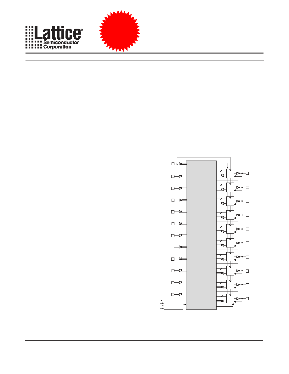
Figure 1. Functional Block Diagram
PROGRAMMABLE
AND-ARRAY
(132X44)
I/O
I/O
I/O
I/O
I/O
I/O
I/O
I/O
I/O
I/O
TDO
TDI
TMS
TCK
I/CLK
I
I
I
I
I
I
I
I
I
I
RESET
PRESET
8
10
12
14
16
16
14
12
10
8
OLMC
OLMC
OLMC
OLMC
OLMC
OLMC
OLMC
OLMC
OLMC
OLMC
PROGRAMMING
LOGIC
I
Lattice Semiconductor
ispGAL22V10AV/B/C Data Sheet
2
ispGAL Architecture
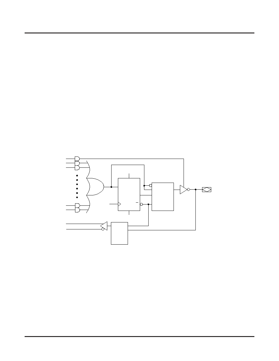
Output Logic Macrocell (OLMC)
The ispGAL22V10A has a variable number of product terms per OLMC. Of the ten available OLMCs, two OLMCs
have access to eight product terms (pins 17 and 27), two have ten product terms (pins 18 and 26), two have twelve
product terms (pins 19 and 25), two have fourteen product terms (pins 20 and 24), and two OLMCs have sixteen
product terms (pins 21 and 23). In addition to the product terms available for logic, each OLMC has an additional
product-term dedicated to output enable control.
The output polarity of each OLMC can be individually programmed to be true or inverting, in either combinatorial or
registered mode. This allows each output to be individually configured as either active high or active low.
The ispGAL22V10A has a product term for Asynchronous Reset (AR) and a product term for Synchronous Preset
(SP). These two product terms are common to all registered OLMCs. The Asynchronous Reset sets all registers to
zero any time this dedicated product term is asserted. The Synchronous Preset sets all registers to a logic one on
the rising edge of the next clock pulse after this product term is asserted.
NOTE: The AR and SP product terms will force the Q output of the flip-flop into the same state regardless of the
polarity of the output. Therefore, a reset operation, which sets the register output to a zero, may result in either a
high or low at the output pin, depending on the pin polarity chosen.
Figure 2. Output Logic Macrocell
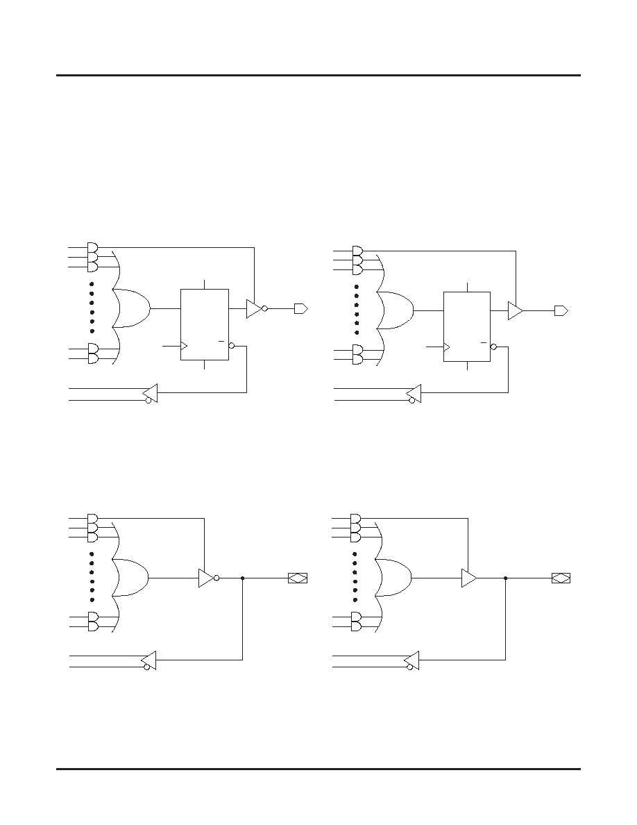
Output Logic Macrocell Configurations
Each of the Macrocells of the ispGAL22V10A has two primary functional modes: registered, and combinatorial I/O.
The modes and the output polarity are set by two bits (S0 and S1), which are normally controlled by the logic com-
piler. Each of these two primary modes, and the bit settings required to enable them, are described below and on
the following page.
Registered
In registered mode the output pin associated with an individual OLMC is driven by the Q output of that OLMC's D-
type flip-flop. Logic polarity of the output signal at the pin may be selected by specifying that the output buffer drive
either true (active high) or inverted (active low). Output tri-state control is available as an individual product-term for
each OLMC, and can therefore be defined by a logic equation. The D flip-flop's /Q output is fed back into the AND
array, with both the true and complement of the feedback available as inputs to the AND array.
AR
SP
D
Q
Q
CLK
4 TO 1
MUX
2 TO 1
MUX
Lattice Semiconductor
ispGAL22V10AV/B/C Data Sheet
3
NOTE: In registered mode, the feedback is from the /Q output of the register, and not from the pin; therefore, a pin
defined as registered is an output only, and cannot be used for dynamic I/O, as can the combinatorial pins.
Combinatorial I/O
In combinatorial mode the pin associated with an individual OLMC is driven by the output of the sum term gate.
Logic polarity of the output signal at the pin may be selected by specifying that the output buffer drive either true
(active high) or inverted (active low). Output tri-state control is available as an individual product-term for each out-
put, and may be individually set by the compiler as either "on" (dedicated output), "off" (dedicated input), or "prod-
uct-term driven" (dynamic I/O). Feedback into the AND array is from the pin side of the output enable buffer. Both
polarities (true and inverted) of the pin are fed back into the AND array.
Figure 3. Registered Mode
Figure 4. Combinatorial Mode
ACTIVE HIGH
ACTIVE LOW
S
0
= 0
S
1
= 0
S
0
= 1
S
1
= 0
AR
SP
D
Q
Q
CLK
AR
SP
D
Q
Q
CLK
ACTIVE HIGH
ACTIVE LOW
S
0
= 1
S
1
= 1
S
0
= 0
S
1
= 1
Lattice Semiconductor
ispGAL22V10AV/B/C Data Sheet
4
Figure 5. Logic Diagram/JEDEC Fuse Map � PLCC & (QFN) Package Pinout
2 (30)
26 (25)
OLMC
S1, S0 = 5810, 5811
SR = 5832
OD = 5833
3 (31)
ASYNCHRONOUS RESET
(TO ALL REGISTERS)
0
JEDEC
Fuse #0
4
8
12
16
20
24
28
32
36
40
SYNCHRONOUS PRESET
(TO ALL REGISTERS)
12 (9)
27 (26)
S1, S0 = 5808, 5809
SR = 5830
OD = 5831
25 (24)
OLMC
S1, S0 = 5812, 5813
SR = 5834
OD = 5835
4 (32)
5 (1)
6 (2)
24 (23)
OLMC
S1, S0 = 5814, 5815
SR = 5836
OD = 5837
23 (22)
OLMC
S1, S0 = 5816, 5817
SR = 5838
OD = 5839
21 (19)
OLMC
S1, S0 = 5818, 5819
SR = 5840
OD = 5841
20 (18)
OLMC
S1, S0 = 5820, 5821
SR = 5842
OD = 5843
OLMC
S1, S0 = 5822, 5823
SR = 5844
OD = 5845
10 (7)
19 (17)
18 (16)
OLMC
S1, S0 = 5824, 5825
SR = 5846
OD = 5847
11 (8)
17 (15)
OLMC
S1, S0 = 5826, 5827
SR = 5848
OD = 5849
9 (6)
7 (3)
13 (10)
16 (14)
8
10
14
16
12
12
16
14
10
8
OLMC
S1, S0 = Arch Control Bits
SR = Slew Rate Bit
OD = Open Drain Bit
JEDEC Fuse #131
JEDEC
Fuse #5676
JEDEC Fuse #5807

Lattice Semiconductor
ispGAL22V10AV/B/C Data Sheet
5
Electronic Signature
An electronic signature (ES) is provided in every ispGAL22V10A device. It contains 32 bits of reprogrammable
memory that can contain user-defined data. Some uses include user ID codes, revision numbers, or inventory con-
trol. The signature data is always available to the user independent of the state of the security cell. IEEE 1149.1
and IEEE 1532 compliant USERCODE is supported.
Low Power and Power Management
The ispGAL22V10A family is designed with high speed low power design techniques to offer both high speed and
low power. With an advanced E
2
low power cell and no sense-amplifiers (full CMOS logic approach), the
ispGAL22V10A family offers fast pin-to-pin speeds, while simultaneously delivering low standby power without
requiring any "turbo bits" or other traditional power-management schemes.
I/O Configuration
Each output supports a variety of output standards dependent on the V
CCO
. Outputs can also be configured for
open drain operation. Each input can be programmed to support a variety of standards, independent of the V
CCO
supplied to its I/O. For 28 PLCC package the V
CCO
and V
CC
must be the same. The option to set the V
CCO
inde-
pendent of V
CC
is available with the 32 QFN package only. The I/O standards supported are:
� LVTTL
� LVCMOS 1.8
� LVCMOS 3.3
� 3.3V PCI Compatible
� LVCMOS 2.5
All of the I/Os and dedicated inputs have the capability to provide a bus-keeper latch, Pull-up Resistor or Pull-down
Resistor. A fourth option is to provide none of these. The selection is done on a global basis. The default in both
hardware and software is such that when the device is erased or if the user does not specify, the input structure is
configured to be a Pull-up Resistor.
Each ispGAL22V10A device I/O has an individually programmable output slew rate control bit. Each output can be
individually configured for the higher speed transition (~3V/ns) or for the lower noise transition (~1V/ns). For high-
speed designs with long, unterminated traces, the slow-slew rate will introduce fewer reflections, less noise and
keep ground bounce to a minimum. For designs with short traces or well terminated lines, the fast slew rate can be
used to achieve the highest speed. The slew rate is adjusted independent of power.
IEEE 1149.1-Compliant Boundary Scan Testability
All ispGAL22V10A devices have boundary scan cells and are compliant to the IEEE 1149.1 standard. This allows
functional testing of the circuit board on which the device is mounted through a serial scan path that can access all
critical logic notes. Internal registers are linked internally, allowing test data to be shifted in and loaded directly onto
test nodes, or test node data to be captured and shifted out for verification. In addition, these devices can be linked
into a board-level serial scan path for more board-level testing. The test access port operates with an LVCMOS
interface that corresponds to the power supply voltage.
IEEE 1532-Compliant In-System Programming
Programming devices in-system provides a number of significant benefits including rapid prototyping, lower inven-
tory levels, higher quality and the ability to make in-field modifications. All ispGAL22V10A devices provide In-Sys-
tem Programming (ISPTM) capability through the Boundary Scan Test Access Port. This capability has been
implemented in a manner that ensures that the port remains complaint to the IEEE 1149.1 standard. By using IEEE
1149.1 as the communication interface through which ISP is achieved, users get the benefit of a standard, well-
defined interface. All ispGAL22V10A devices are also compliant with the IEEE 1532 standard.
The ispGAL22V10A devices can be programmed across the commercial temperature and voltage range. The PC-
based Lattice software facilitates in-system programming of ispGAL22V10A devices. The software takes the
JEDEC file output produced by the design implementation software, along with information about the scan chain,
and creates a set of vectors used to drive the scan chain. The software can use these vectors to drive a scan chain
Lattice Semiconductor
ispGAL22V10AV/B/C Data Sheet
6
via the parallel port of a PC. Alternatively, the software can output files in formats understood by common auto-
mated test equipment. This equipment can then be used to program ispGAL22V10A devices during the testing of a
circuit board.
Security Bit
A programmable security bit is provided on the ispGAL22V10A devices as a deterrent to unauthorized copying of
the array configuration patterns. Once programmed, this bit defeats readback of the programmed pattern by a
device programmer, securing proprietary designs from competitors. Programming and verification are also
defeated by the security bit. The bit can only be reset by erasing the entire device.
Hot Socketing
The ispGAL22V10A devices are well-suited for applications that require hot socketing. Hot socketing a device
requires that the device, during power-up and down, tolerate active signals on the I/Os and inputs without being
damaged. Additionally, it requires that the effects of I/O pin loading be minimal on active signals. The
ispGAL22V10A devices provide this capability for input voltages in the range of 0V to 3.0V.
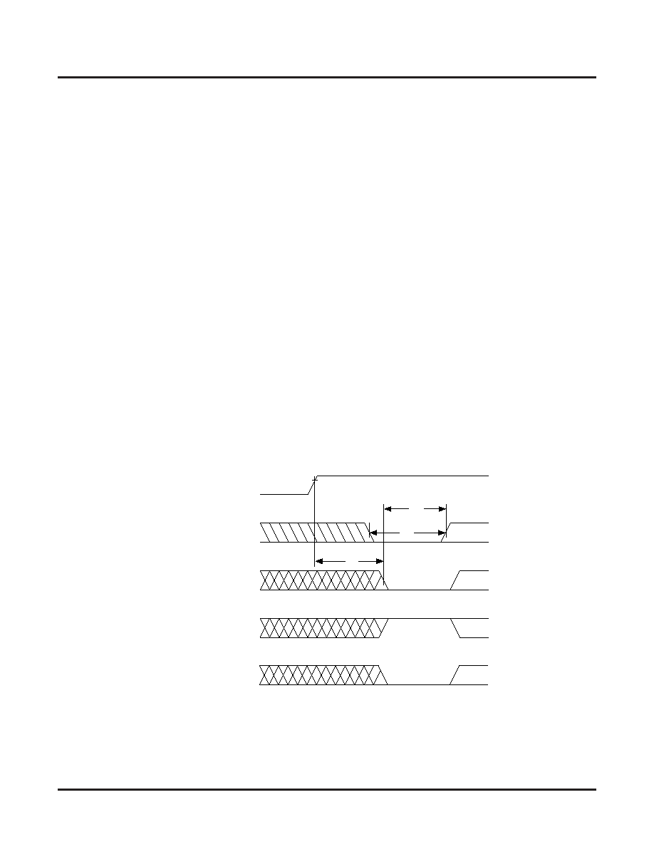
Power-up Reset
Circuitry within the ispGAL22V10A provides a reset signal to all registers during power-up. All internal registers will
have their Q outputs set low after a specified time (tpr, 1�s typical). As a result, the state on the registered output
pins (if they are enabled) will be either high or low on power-up, depending on the programmed polarity of the out-
put pins. This feature can greatly simplify state machine design by providing a known state on power-up. The timing
diagram for power-up is shown above. Because of the asynchronous nature of system power-up, some conditions
must be met to provide a valid power-up reset of the ispGAL22V10A. First, the Vcc rise must be monotonic. Sec-
ond, the clock input must be at static TTL level as shown in the diagram during power up. The registers will reset
within a maximum of tpr time. As in normal system operation, avoid clocking the device until all input and feedback
path setup times have been met. The clock must also meet the minimum pulse width requirements.
Figure 6. Timing Diagram for Power-up
Vcc (min.)
t
pr
Internal Register
Reset to Logic "0"
Device Pin
Reset to Logic "1"
t
wl
t
su
Device Pin
Reset to Logic "0"
V c c
C L K
INTERNAL REGISTER
Q - OUTPUT
ACTIVE LOW
OUTPUT REGISTER
ACTIVE HIGH
OUTPUT REGISTER
Lattice Semiconductor
ispGAL22V10AV/B/C Data Sheet
7
Absolute Maximum Ratings
1, 2, 3
ispGAL
ispGAL ispGAL
22V10AC (1.8V)
22V10AB (2.5V)
22V10AV (3.3V)
Supply Voltage V
CC
. . . . . . . . . . . . . . . . . . . . . . . . -0.5 to 2.5V
-0.5 to 5.5V
-0.5 to 5.5V
Output Supply Voltage V
CCO
. . . . . . . . . . . . . . . . . -0.5 to 4.5V
-0.5 to 4.5V
-0.5 to 4.5V
Input or I/O Tristate Voltage Applied
4
. . . . . . . . . . . -0.5 to 5.5V
-0.5 to 5.5V
-0.5 to 5.5V
Storage Temperature . . . . . . . . . . . . . . . . . . . . . . . -65 to 150
�
C
-65 to 150
�
C
-65 to 150
�
C
Junction Temperature (T
j
) with Power Applied . . . . -55 to 150
�
C
-55 to 150
�
C
-55 to 150
�
C
1. Stress above those listed under the "Absolute Maximum Ratings" may cause permanent damage to the device. Functional
operation of the device at these or any other conditions above those indicated in the operational sections of this specification
is not implied.
2. Compliance with Lattice
Thermal Management
document is required.
3. All voltages referenced to GND.
4. Undershoot of -2V and overshoot of (V
IH
(MAX) +2), up to a total pin voltage of 6.0V, is permitted for a duration of < 20ns.
Recommended Operating Conditions
Erase Reprogram Specifications
Hot Socketing Characteristics
1,2,3
I/O Recommended Operating Conditions
Symbol
Parameter
Min
Max
Units
V
CC
Supply Voltage for 1.8V Devices
1.65
1.95
V
Supply Voltage for 2.5V Devices
2.3
2.7
V
Supply Voltage for 3.3V Devices
3.0
3.6
V
T
j
Junction Temperature (Commercial)
0
90
C
Junction Temperature (Industrial)
-40
105
C
Parameter
Min
Max
Units
Erase/Reprogram Cycle
1,000
--
Cycles
Note: Valid over commercial temperature range.
Symbol
Parameter
Condition
Min
Typ
Max
Units
I
DK
Input or I/O Leakage Current
0
V
IN
3.0V, T
j
= 105�C
--
--
�50
�
A
1. Insensitive to sequence of V
CC
and V
CCO
. However, assumes monotonic rise/fall rates for V
CC
and V
CCO
, provided (V
IN
- V
CCO
)
3.0V.
2. 0
V
CC
V
CC
(MAX), 0
V
CCO
V
CCO
(MAX)
3. I
DK
is additive to I
PU
, I
PD
or I
BH
. Device defaults to pull-up until fuse circuitry is active.
Standard
V
CCO
(V)
1
Min
Max
LVTTL
3.0
3.6
LVCMOS 3.3
3.0
3.6
LVCMOS 2.5
2.3
2.7
LVCMOS 1.8
1.65
1.95
PCI 3.3
3.0
3.6
1. Typical values for V
CCO
are the average of the Min and Max values.
Lattice Semiconductor
ispGAL22V10AV/B/C Data Sheet
8
DC Electrical Characteristics
Over Recommended Operating Conditions
Symbol
Parameter
Condition
Min
Typ
Max
Units
I
IL
, I
IH
1
Input Leakage Current
0 < V
IN
3.6V, T
j
= 105�C
--
--
10
�A
I
IH
2
Input High Leakage Current
3.6V < V
IN
5.5V, T
j
= 105�C
3.0V
V
CCO
3.6V
--
--
20
�A
I
OS
Output Short Circuit Current
V
CC
= 3.3V, V
OUT
= 0.5V,
T
A
= 25�C
--
--
-80
mA
I
PU
I/O Weak Pull-up Resistor Current
0
V
IN
0.7V
CCO
20
--
150
�A
I
PD
I/O Weak Pull-down Resistor Current V
IL
(MAX)
V
IN
V
IH
(MAX)
20
--
150
�A
I
BHLS
Bus Hold Low Sustaining Current
V
IN
= V
IL
(MAX)
20
--
--
�A
I
BHHS
Bus Hold High Sustaining Current
V
IN
= 0.7 V
CCO
20
--
--
�A
I
BHLO
Bus Hold Low Overdrive Current
0V
V
IN
V
IH
(MAX)
--
--
150
�A
I
BHHO
Bus Hold High Overdrive Current
0
V
IN
V
IH
(MAX)
--
--
150
�A
V
BHT
Bus Hold Trip Points
--
V
IL
(MAX)
--
V
IH
(MIN)
V
C
1
I/O Capacitance
3
V
CCO
= 3.3V, 2.5V, 1.8V
--
6
--
pf
V
CC
= 1.8V, V
IO
= 0 to V
IH
(MAX)
--
--
C
2
Clock Capacitance
3
V
CCO
= 3.3V, 2.5V, 1.8V
--
8
--
pf
V
CC
= 1.8V, V
IO
= 0 to V
IH
(MAX)
--
--
1. Input or I/O leakage current is measured with the pin configured as an input or as an I/O with the output driver tristated. It is not
measured with the output driver active. Bus maintenance circuits are disabled.
2. 5 volt tolerant inputs and I/Os apply to V
CCO
condition of 3.0V
V
CCO
3.6V.
3. T
A
= 25�C, frequency = 1.0MHz
Supply Current
Over Recommended Operating Conditions
Symbol
Parameter
Condition
Min
Typ
Max
Units
ispGAL22V10AV/B/C
I
CC
1, 2
Operating Power Supply Current
V
CC
= 3.3V
--
8
90
mA
V
CC
= 2.5V
--
8
90
mA
V
CC
= 1.8V
--
3
80
mA
I
CC
3
Standby Power Supply Current
V
CC
= 3.3V
--
7
--
mA
V
CC
= 2.5V
--
7
--
mA
V
CC
= 1.8V
--
150
--
�A
1. T
A
= 25
�
C, frequency = 15MHz.
2. I
CC
varies with specific device configuration and operating frequency.
3. T
A
= 25
�
C
Lattice Semiconductor
ispGAL22V10AV/B/C Data Sheet
9
I/O DC Electrical Characteristics
1
Over Recommended Operating Conditions
Standard
V
IL
V
IH
V
OL
Max (V)
V
OH
Min (V)
I
OL
(mA)
I
OH
(mA)
Min (V)
Max (V)
Min (V)
Max (V)
LVTTL
-0.3
0.80
2.0
5.5
0.40
V
CCO
- 0.40
8.0
-4.0
0.20
V
CCO
- 0.20
0.1
-0.1
LVCMOS 3.3
-0.3
0.80
2.0
5.5
0.40
V
CCO
- 0.40
8.0
-4.0
0.20
V
CCO
- 0.20
0.1
-0.1
LVCMOS 2.5
-0.3
0.70
1.70
3.6
0.40
V
CCO
- 0.40
8.0
-4.0
0.20
V
CCO
- 0.20
0.1
-0.1
LVCMOS 1.8
(ispGAL22V10AV/B)
-0.3
0.63
1.17
3.6
0.40
V
CCO
- 0.45
2.0
-2.0
0.20
V
CCO
- 0.20
0.1
-0.1
LVCMOS 1.8
(ispGAL22V10AC)
-0.3
0.35 V
CC
0.65 * V
CC
3.6
0.40
V
CCO
- 0.45
2.0
-2.0
0.20
V
CCO
- 0.20
0.1
-0.1
PCI 3.3
(ispGAL22V10AV/B)
-0.3
1.08
1.5
5.5
0.1 V
CCO
0.9 V
CCO
1.5
-0.5
PCI 3.3
(ispGAL22V10AC)
-0.3
0.3 * 3.3 * (V
CC
/
1.8) 0.5 * 3.3 * (V
CC
/
1.8)
5.5
0.1 V
CCO
0.9 V
CCO
1.5
-0.5
1. For 28 PLCC package the I/O voltage and core voltage must be the same. The option to set the I/O voltage independent of the core voltage
is available with the 32 QFN package only.
V
O
Output Voltage (V)
Typical I/O Output Current (mA)
3.3V V
CCO
V
O
Output Voltage (V)
0
0
0
20
40
60
80
100
10
20
30
40
50
60
0
10
20
30
40
50
60
70
2.0
1.5
1.0
0.5
0
2.0 2.5
3.0 3.5
1.5
1.0
0.5
0
2.0
2.5
1.5
1.0
0.5
Typical I/O Output Current (mA)
1.8V V
CCO
V
O
Output Voltage (V)
I
OH
Typical I/O Output Current (mA)
2.5V V
CCO
I
OL
I
OH
I
OL
I
OH
I
OL
Lattice Semiconductor
ispGAL22V10AV/B/C Data Sheet
10
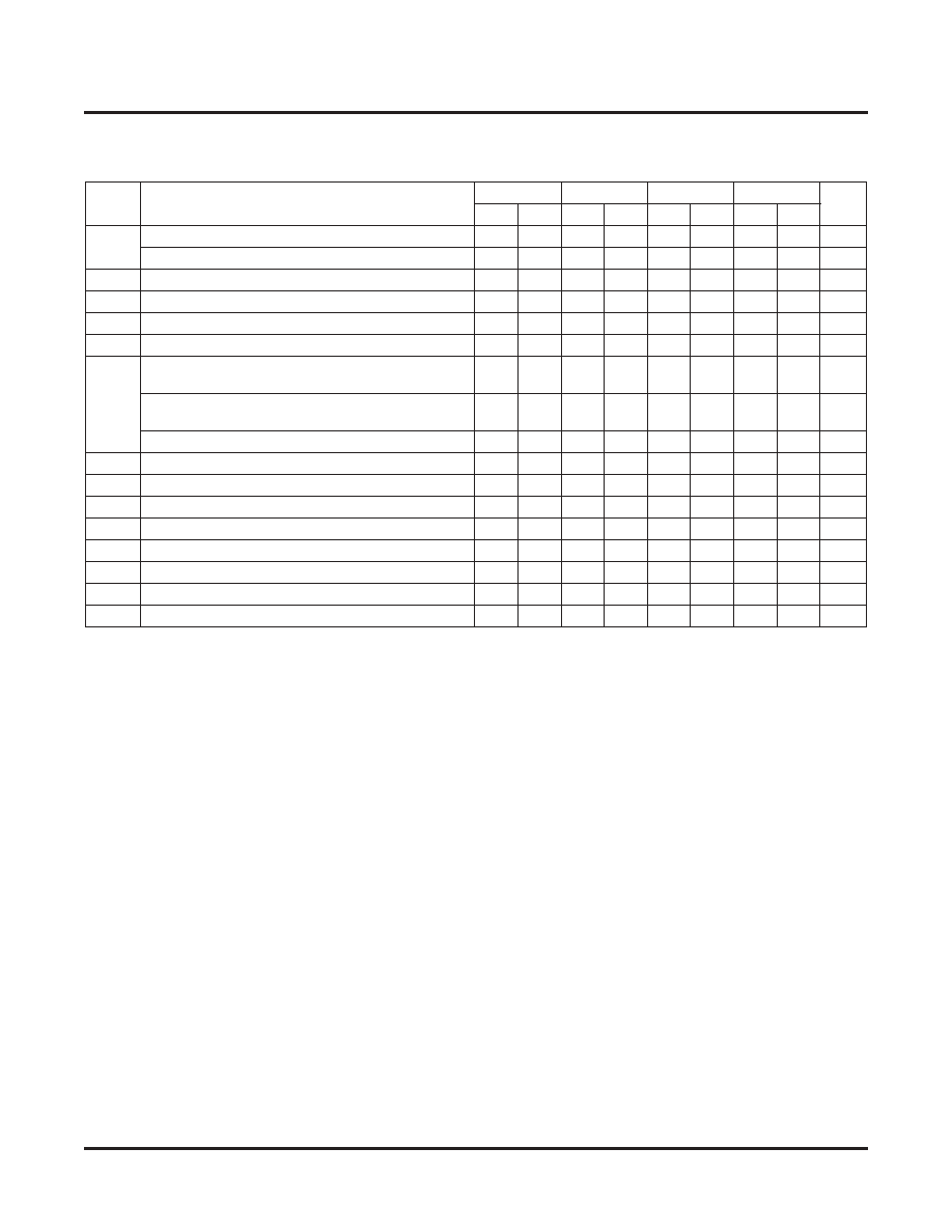
ispGAL22V10AV/B/C External Switching Characteristics (Preliminary)
1
Over Recommended Operating Conditions
Param
Description
-23
-28
-5
-75
Units
Min
Max
Min
Max
Min
Max
Min
Max
t
PD
1 Output Switching Propagation Delay
--
2.3
--
2.8
--
--
--
--
ns
10 Output Switching Propagation Delay
--
2.6
--
3.0
--
5.0
--
7.5
t
CO
Clock to Output Delay
--
2.0
--
2.5
--
3.5
--
5.0
ns
t
CF
2
Clock to Feedback Delay
--
1.9
--
2.2
--
2.5
--
2.5
ns
t
SU
Setup Time, Input or Feedback before CLK
1.3
--
2.0
--
3.5
--
5.0
--
ns
t
H
Hold Time, Input or Feedback after CLK
0
--
0
--
0
--
0
--
ns
f
MAX
3
Maximum Clock Frequency with External Feedback,
[1/ (t
SU
+ t
CO
)]
303
--
222
--
143
--
100
--
ns
Maximum Clock Frequency with Internal Feedback,
[1/ (t
SU
+ t
CF
)]
312
--
238
--
166
--
133
--
ns
Maximum Clock Frequency with No Feedback
455
--
357
--
200
--
166
--
ns
t
WH
3
Clock Pulse Duration, High
1.1
--
1.4
--
2.5
--
3.0
--
ns
t
WL
3
Clock Pulse Duration, Low
1.1
--
1.4
--
2.5
--
3.0
--
ns
t
EN
Input or I/O to Output Enabled
--
3.0
--
3.5
--
6.0
--
7.5
ns
t
DIS
Input or I/O to Output Disabled
--
3.0
--
3.5
--
6.0
--
7.5
ns
t
AR
Input or I/O to Asynch, Reset of Reg.
--
2.8
--
3.5
--
5.5
--
9.0
ns
t
ARW
Asysnchronous Reset Pulse Duration
2.8
--
3.5
--
5.5
--
7.0
--
ns
t
ARR
Asysnchronous Reset to CLK
Recovery Time
2.5
--
3.0
--
4.0
--
5.0
--
ns
t
SPR
Synchronous Preset to CLK
Recovery Time
2.5
--
3.0
--
4.0
--
5.0
--
ns
1. Refer to Switching Test Conditions section.
2. Calculated from fmax with internal feedback. Refer to fmax Descriptions section.
3. Refer to fmax Descriptions section. Characterized but not 100% tested.
Note: Maximum clock input rise and fall time between 10% to 90% of Vout = 2ns.
Lattice Semiconductor
ispGAL22V10AV/B/C Data Sheet
11
ispGAL22V10AV/B/C Timing Adders
Over Recommended Operating Conditions
Adder
Type
Description
-23
-28
-5
-75
Units
Min.
Max.
Min.
Max.
Min.
Max.
Min.
Max.
t
IOI
Input Adjusters
LVTTL_in
Using LVTTL standard
--
0.6
--
0.6
--
0.6
--
0.6
ns
LVCMOS33_in
Using LVCMOS 3.3
standard
--
0.6
--
0.6
--
0.6
--
0.6
ns
LVCMOS25_in
Using LVCMOS 2.5
standard
--
0.6
--
0.6
--
0.6
--
0.6
ns
LVCMOS18_in
Using LVCMOS 1.8
standard
--
0
--
0
--
0
--
0
ns
PCI_in
Using PCI compatible input
--
0.6
--
0.6
--
0.6
--
0.6
ns
t
IOO
Output Adjusters
LVTTL_out
Output configured as TTL buffer
--
0.2
--
0.2
--
0.2
--
0.2
ns
LVCMOS33_out Output configured as 3.3V buffer
--
0.2
--
0.2
--
0.2
--
0.2
ns
LVCMOS25_out Output configured as 2.5V buffer
--
0.1
--
0.1
--
0.1
--
0.1
ns
LVCMOS18_out Output configured as 1.8V buffer
--
0
--
0
--
0
--
0
ns
PCI_out
Output configured as
PCI compatible buffer
--
0.2
--
0.2
--
0.2
--
0.2
ns
Slow Slew
Output configured for slow slew rate
--
1.0
--
1.0
--
1.0
--
1.0
ns
Note: Open drain timing is the same as corresponding LVCMOS timing.
Lattice Semiconductor
ispGAL22V10AV/B/C Data Sheet
12
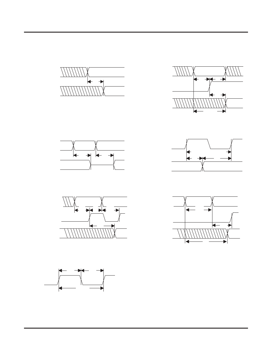
Switching Waveforms
Figure 7. ispGAL22V10AV/B/C Switching Waveforms
INPUT or
I/O FEEDBACK
REGISTERED
OUTPUT
CLK
VALID INPUT
t
s u
t
c o
t
h
(external fdbk)
1 /
f
m a x
VALID IN PU T
INPU T or
I/O F EEDB ACK
t
p d
CO MB INA T O R I AL
O U T P U T
CLK
REGISTERED
FEEDBACK
t
c f
t
su
1 /
f
m a x ( i n t e r n a l f d b k )
CLK
(w/o fdbk)
t
w h
t
w l
1 /
f
m a x
REGISTERED
OUTPUT
C L K
t
arw
t
arr
INPUT or
I/O FEEDBACK
DRIVING AR
t
ar
REGISTERED
OUTPUT
CLK
INPUT or
I/O FEEDBACK
DRIVING SP
t
su
t
h
t
co
t
spr
t
en
t
dis
INPUT or
I/O FEEDBACK
OUTPUT
Combinatorial Output
Registered Output
Input or I/O to Output Enable/Disable
f
MAX
with Feedback
Synchronous Preset
Clock Width
Asynchronous Reset
Lattice Semiconductor
ispGAL22V10AV/B/C Data Sheet
13
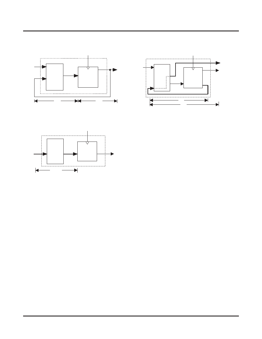
f
MAX
Descriptions
Figure 8. ispGAL22V10AV/B/C f
MAX
Descriptions
R E G I S T E R
L O G I C
A R R A Y
t
c o
t
s u
C L K
REGISTER
LOGIC
ARRAY
CLK
t
su +
t
h
CLK
REGISTER
LOGIC
ARRAY
t
cf
t
pd
Note: tcf is a calculated value, derived by
subtracting tsu from the period of fmax
w/internal feedback (tcf = 1/fmax - tsu). The
value of tcf is used primarily when
calculating the delay from clocking a
register to a combinatorial output (through
registered feedback), as shown above. For
example, the timing from clock to a
combinatorial output is equal to tcf + tpd.
Note: fmax with external feedback is
calculated from measured tsu and tco.
Note: fmax with no feedback may be less
than 1/twh + twl. This is to allow for a clock
duty cycle of other than 50%.
fmax with Internal Feedback 1/(tsu+tcf)
fmax with External Feedback 1/(tsu+tco)
fmax with No Feedback
Lattice Semiconductor
ispGAL22V10AV/B/C Data Sheet
14
Switching Test Conditions
Figure 9 shows the output test load that is used for AC testing. The specific values for resistance, capacitance, volt-
age, and other test conditions are shown in Table 1.
Figure 9. Output Test Load, LVTTL and LVCMOS Standards
Table 1. Test Fixture Required Components
Pin Diagrams
Test Condition
I/O Standare
R
1
R
2
C
L
1
Input
Timing Ref.
2
Output
Timing Ref.
V
CCO
LVCMOS I/O, (L -> H, H -> L)
LVCMOS 3.3
106
106
35pF
1.5V
1.5V
3.0V
LVCMOS 2.5
1.2V
V
CCO
/2
2.3V
LVCMOS 1.8
(V/B) 0.9V
V
CCO
/2
(V/B) 1.65V
(C) V
CC
/2
V
CCO
/2
(C) V
CC
LVCMOS I/O (Z -> H)
106
106
35pF
Hi-Z + 0.3
3.0V
LVCMOS I/O (Z -> L)
106
106
35pF
Hi-Z - 0.3
3.0V
LVCMOS I/O (H -> Z)
106
5pF
V
OH
- 0.3
3.0V
LVCMOS I/O (L -> Z)
106
5pF
V
OL
+ 0.3
3.0V
1. C
L
includes test fixtures and probe capacitance.
2. Input conditions.
V
CCO
R1
R2
CL
DUT
Test
Point
29 28
TCK
I/CLK
I
I
I
I
I
Vcco
I
I
TMS
TDO
GNDO
GND
I
I
TDI
I/O
I
I/O
I
I/O
I/O
GNDO
Top View
QFN
I/O
I/O
I/O
Vcc
I/O
I/O
I/O
Vcco
32
25
24
17
16
20
21
13
12
9
8
5
4
1
2
28
TCK
I/CLK
I
I
I
I
I
I
I
I
TMS
TDO
TDI
GND
I
I
I
I/O
I/O
I/O
I/O
I/O
I/O
I/O
Vcc
I/O
I/O
I/O
4
26
25
19
18
21
23
16
14
12
11
9
7
5
Top View
PLCC
Lattice Semiconductor
ispGAL22V10AV/B/C Data Sheet
15
Part Number Description
Ordering Information
Commercial
Part Number
Voltage
t
PD
Power
Package
Pin Count
Grade
ispGAL22V10AV-23LN
3.3
2.3ns
Low
QFN
32
C
ispGAL22V10AV-5LN
3.3
5.0ns
Low
QFN
32
C
ispGAL22V10AV-75LN
3.3
7.5ns
Low
QFN
32
C
ispGAL22V10AV-28LJ
3.3
2.8ns
Low
PLCC
28
C
ispGAL22V10AV-5LJ
3.3
5.0ns
Low
PLCC
28
C
ispGAL22V10AV-75LJ
3.3
7.5ns
Low
PLCC
28
C
ispGAL22V10AB-23LN
2.5
2.3ns
Low
QFN
32
C
ispGAL22V10AB-5LN
2.5
5.0ns
Low
QFN
32
C
ispGAL22V10AB-75LN
2.5
7.5ns
Low
QFN
32
C
ispGAL22V10AB-28LJ
2.5
2.8ns
Low
PLCC
28
C
ispGAL22V10AB-5LJ
2.5
5.0ns
Low
PLCC
28
C
ispGAL22V10AB-75LJ
2.5
7.5ns
Low
PLCC
28
C
ispGAL22V10AC-23LN
1.8
2.3ns
Low
QFN
32
C
ispGAL22V10AC-5LN
1.8
5.0ns
Low
QFN
32
C
ispGAL22V10AC-75LN
1.8
7.5ns
Low
QFN
32
C
ispGAL22V10AC-28LJ
1.8
2.8ns
Low
PLCC
28
C
ispGAL22V10AC-5LJ
1.8
5.0ns
Low
PLCC
28
C
ispGAL22V10AC-75LJ
1.8
7.5ns
Low
PLCC
28
C
Industrial
Part Number
Voltage
t
PD
Power
Package
Pin Count
Grade
ispGAL22V10AV-5LNI
3.3
5.0ns
Low
QFN
32
I
ispGAL22V10AV-75LNI
3.3
7.5ns
Low
QFN
32
I
ispGAL22V10AV-5LJI
3.3
5.0ns
Low
PLCC
28
I
ispGAL22V10AV-75LJI
3.3
7.5ns
Low
PLCC
28
I
ispGAL22V10AB-5LNI
2.5
5.0ns
Low
QFN
32
I
ispGAL22V10AB-75LNI
2.5
7.5ns
Low
QFN
32
I
ispGAL22V10AB-5LJI
2.5
5.0ns
Low
PLCC
28
I
ispGAL22V10AB-75LJI
2.5
7.5ns
Low
PLCC
28
I
Device Number
ispGAL 22V10A X � XX X X X
Supply Voltage
V = 3.3V
B = 2.5V
C = 1.8V
Speed
23 = 2.3ns
28 = 2.8ns
5 = 5.0ns
75 = 7.5ns
Package
J = PLCC (28 pins)
N = QFN (32 pins)
Grade
C = Commercial
I = Industrial
Device Family
Power
L = Low Power
Lattice Semiconductor
ispGAL22V10AV/B/C Data Sheet
16
Note: For all but the slowest commercial speed grade, the speed grades on these devices are dual marked. For
example, the commercial speed grade -5LJ is also marked with the industrial grade -7LJI. The commercial grade is
always one speed grade faster than the associated dual mark industrial grade. The slowest commercial speed
grade is marked as commercial grade only.
ispGAL22V10AC-5LNI
1.8
5.0ns
Low
QFN
32
I
ispGAL22V10AC-75LNI
1.8
7.5ns
Low
QFN
32
I
ispGAL22V10AC-5LJI
1.8
5.0ns
Low
PLCC
28
I
ispGAL22V10AC-75LJI
1.8
7.5ns
Low
PLCC
28
I
Industrial (Cont.)
Part Number
Voltage
t
PD
Power
Package
Pin Count
Grade