Document Outline
- Table of Contents
- ispGDX Family Data Sheet
- DC Electrical Characteristics
- AC Specifications
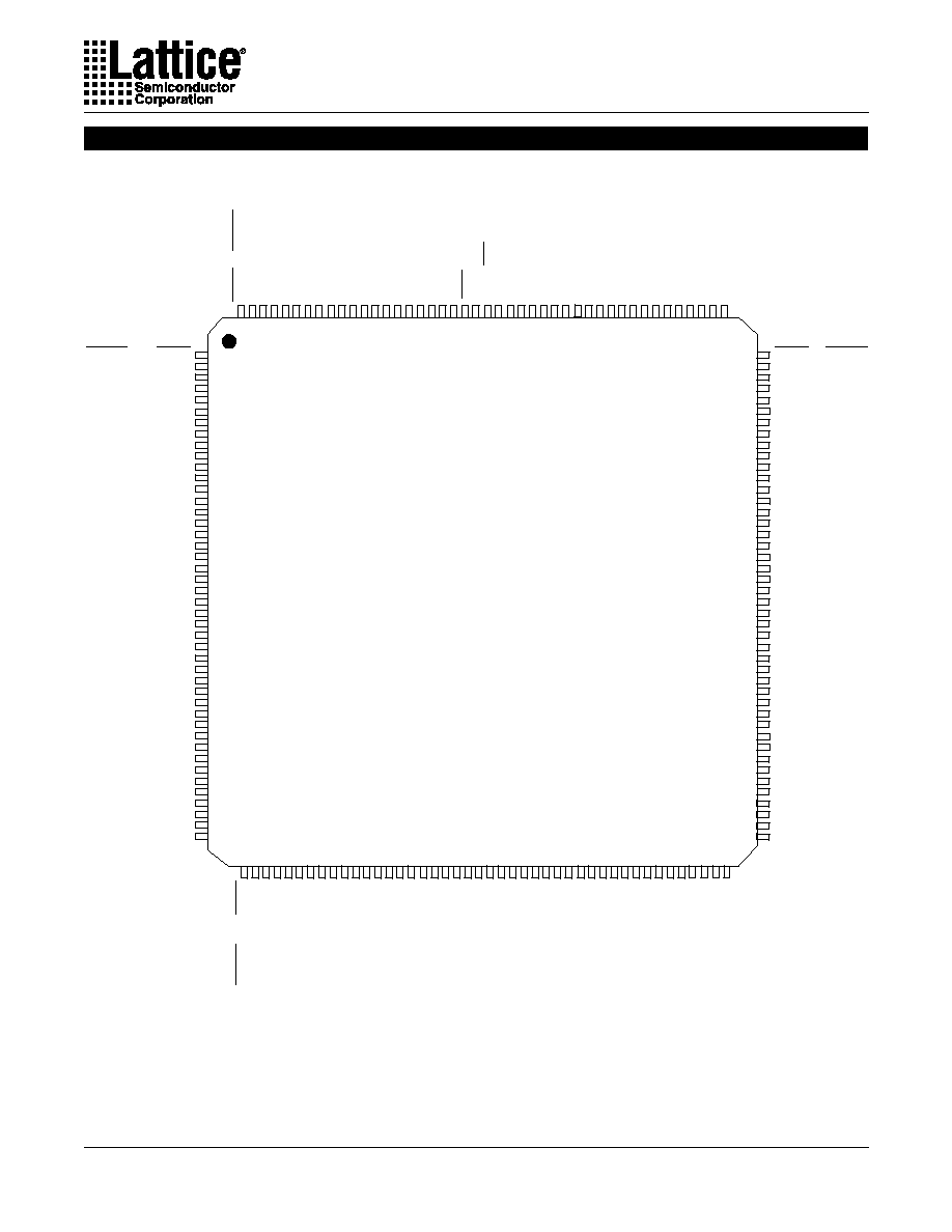
- Signal Configuration: 272-Ball BGA
- Pin Configuration: 208-Pin PQFP
- Pin Configuration: 176-Pin TQFP
- Pin Configuration: 160-Pin PQFP
- Pin Configuration: 100-Pin TQFP
- Ordering Information
ispGDX
TM
Family
In-System Programmable
Generic Digital Crosspoint
TM
ispgdx_08
1
Functional Block Diagram
Features
∑ IN-SYSTEM PROGRAMMABLE GENERIC DIGITAL
CROSSPOINT FAMILY
-- Advanced Architecture Addresses Programmable
PCB Interconnect, Bus Interface Integration and
Jumper/Switch Replacement
-- Three Device Options: 80 to 160 Programmable I/O
Pins
-- "Any Input to Any Output" Routing
-- Fixed HIGH or LOW Output Option for Jumper/DIP
Switch Emulation
-- Space-Saving TQFP, PQFP and BGA Packaging
-- Dedicated IEEE 1149.1-Compliant Boundary Scan
Test
-- PCI Compliant Output Drive
∑ HIGH PERFORMANCE E
2
CMOS
Æ
TECHNOLOGY
-- 5V Power Supply
-- 5.0ns Input-to-Output/5.0ns Clock-to-Output Delay
-- Low-Power: 40mA Quiescent Icc
-- Balanced 24mA Output Buffers with Programmable
Slew Rate Control
-- Schmitt Trigger Inputs for Noise Immunity
-- Electrically Erasable and Reprogrammable
-- Non-Volatile E
2
CMOS Technology
-- 100% Tested
∑ ispGDX OFFERS THE FOLLOWING ADVANTAGES
-- In-System Programmable
-- Lattice ISP or JTAG Programming Interface
-- Only 5V Power Supply Required
-- Change Interconnects in Seconds
-- Reprogram Soldered Devices
∑ FLEXIBLE ARCHITECTURE
-- Combinatorial/Latched/Registered Inputs or Outputs
-- Individual I/O Tri-state Control with Polarity Control
-- Dedicated Clock Input Pins (two or four) or
Programmable Clocks from I/O Pins (from 20 up to
40)
-- Up to 4:1 Dynamic Path Selection
-- Programmable Output Pull-up Resistors
-- Outputs Tri-state During Power-up ("Live Insertion"
Friendly)
∑ DESIGN SUPPORT THROUGH LATTICE'S ispGDX
DEVELOPMENT SOFTWARE
-- MS Windows or NT / PC-Based or Sun O/S
-- Easy Text-Based Design Entry
-- Automatic Signal Routing
-- Program up to 100 ISP Devices Concurrently
-- Simulator Netlist Generation for Easy Board-Level
Simulation
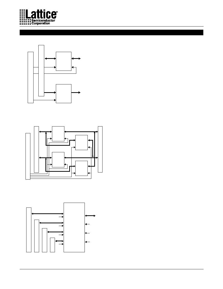
Global Routing
Pool
(GRP)
I/O
Cells
I/O Pins B
Boundary
Scan
Control
I/O
Cells
ISP
Control
I/O Pins
A
I/O Pins C
I/O Pins D
Description
The ispGDX architecture provides a family of fast, flexible
programmable devices to address a variety of system-
level digital signal routing and interface requirements
including:
∑ Multi-Port Multiprocessor Interfaces
∑ Wide Data and Address Bus Multiplexing
(e.g. 4:1 High-Speed Bus MUX)
∑ Programmable Control Signal Routing
(e.g. Interrupts, DMAREQs, etc)
∑ Board-Level PCB Signal Routing for Prototyping or
Programmable Bus Interfaces
The ispGDX Family consists of three members with 80,
120 and 160 Programmable I/Os. These devices are
available in packages ranging from the 100-pin TQFP to
the 208-pin PQFP. The devices feature fast operation,
with input-to-output signal delays (Tpd) of 5ns and clock-
to-output delays of 5ns.
The architecture of the devices consists of a series of
programmable I/O cells interconnected by a Global Rout-
Copyright © 2000 Lattice Semiconductor Corporation. All brand or product names are trademarks or registered trademarks of their respective holders. The specifications and information herein
are subject to change without notice.
LATTICE SEMICONDUCTOR CORP., 5555 Northeast Moore Ct., Hillsboro, Oregon 97124, U.S.A.
August 2000
Tel. (503) 268-8000; 1-800-LATTICE; FAX (503) 268-8556; http://www.latticesemi.com
2
Specifications
ispGDX Family
Description (Continued)
ing Pool (GRP). All I/O pin inputs enter the GRP directly
or are registered or latched so they can be routed to the
required I/O outputs. I/O pin inputs are defined as four
sets (A,B,C,D) which have access to the four MUX inputs
found in each I/O cell. Each output has individual, pro-
grammable I/O tri-state control (OE), output latch clock
(CLK) and two multiplexer control (MUX0 and MUX1)
inputs. Polarity for these signals is programmable for
each I/O cell. The MUX0 and MUX1 inputs control a fast
4:1 MUX, allowing dynamic selection of up to four signal
sources for a given output. OE, CLK and MUX0 and
MUX1 inputs can be driven directly from selected sets of
I/O pins. Optional dedicated clock input pins give mini-
mum clock-to-output delays.
Through in-system programming, connections between
I/O pins and architectural features (latched or registered
inputs or outputs, output enable control, etc.) can be
defined. In keeping with its data path application focus,
the ispGDX devices contain no programmable logic
arrays. All input pins include Schmitt trigger buffers for
noise immunity. These connections are programmed
into the device using non-volatile E
2
CMOS technology.
Non-volatile technology means the device configuration
is saved even when the power is removed from the
device.
In addition, there are no pin-to-pin routing constraints for
1:1 or 1:n signal routing. That is,
any I/O pin configured
as an input can drive one or more I/O pins configured as
outputs.
The device pins also have the ability to set outputs to
fixed HIGH or LOW logic levels (Jumper or DIP Switch
mode). Device outputs are specified for 24mA sink and
source current and can be tied together in parallel for
greater drive. Programmable output slew rate can be
defined independently for each I/O pin to reduce overall
ground bounce and switching noise.
All I/O pins are equipped with IEEE1149.1-compliant
Boundary Scan Test circuitry for enhanced testability. In
addition, in-system programming is supported through
the Test Access Port via a special set of private com-
mands or through Lattice's industry-standard ISP protocol.
The BSCAN/
ispEN
pin is used to make this selection.
The ispGDX I/Os are designed to withstand "live inser-
tion" system environments. The I/O buffers are disabled
during power-up and power-down cycles. When design-
ing for "live insertion," absolute maximum rating conditions
for the Vcc and I/O pins must still be met. For additional
information, an application note about using Lattice de-
vices in hot swap environments can be downloaded from
the Lattice web site at www.latticesemi.com.
Table 1. ispGDX Family Members
ispGDX DEVICE
ispGDX80A
ispGDX120A
ispGDX160/A
I/O Pins
80
120
160
I/O-OE Inputs*
20
30
40
I/O-Clk Inputs*
20
30
40
I/O-MUXsel1 Inputs*
20
30
40
I/O-MUXsel2 Inputs*
20
30
40
BSCAN / ISP Interface
4
4
4
RESET
1
1
1
Power/GND
12
25
33
Pin Count/Package
100-Pin TQFP
176-Pin TQFP/
160-Pin PQFP
208-Pin PQFP
272-Ball BGA
* The CLK, OE, MUX0 and MUX1 terminals on each I/O cell can each access 25% of the I/Os.
** MUXed with Y1.
TOE
1**
1
1
Dedicated Clock Pins
2
4
4
BSCAN /
ispEN
1
1
1
3
Specifications
ispGDX Family
Architecture
The ispGDX architecture is different from traditional PLD
architectures, in keeping with its unique application fo-
cus. The block diagram is shown below. The
programmable interconnect consists of a single Global
Routing Pool (GRP). Unlike ispLSI devices, there are no
programmable logic arrays on the device. Control signals
for OEs, Clocks and MUX Controls must come from
designated sets of I/O pins. The polarity of these signals
can be independently programmed in each I/O cell.
Each I/O cell drives a unique pin. The OE control for each
I/O pin is independent and may be driven via the GRP by
one of the designated I/O pins (I/O-OE set). The I/O-OE
set consists of 25% of the total I/O pins. Boundary Scan
test is supported by dedicated registers at each I/O pin.
The in-system programming process uses either a Bound-
ary Scan based or Lattice ISP protocol. The programming
protocol is selected by the BSCAN/
ispEN
pin as de-
scribed later.
The various I/O pin sets are also shown in the block
diagram below. The A, B, C, and D I/O pins are grouped
together with one group per side.
I/O Architecture
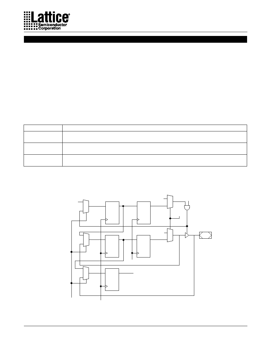
Each I/O cell contains a 4:1 dynamic MUX controlled by
two select lines called MUX0 and MUX1 as shown in
Figure 1. The four data inputs to the MUX (called MUXA,
MUXB, MUXC and MUXD) come from I/O signals found
in the GRP. Each MUX data input can access one quarter
of the total I/Os. For example, in a 160 I/O ispGDX, each
data input can connect to one of 40 I/O pins. MUX0 and
MUX1 can be driven by designated I/O pins called
MUXsel1 and MUXsel2. Each MUXsel input covers 25%
of the total I/O pins (e.g. 40 out of 160). MUX0 and MUX1
can be driven from either MUXsel1 or MUXsel2. The I/O
cell also includes a programmable flow-through latch or
register that can be placed in the input or output path and
bypassed for combinatorial outputs. As shown in Figure
1, when both register/latch control MUXes select the "A"
path, the register/latch gets its inputs from the 4:1 MUX
and drives the I/O output. When selecting the "B" path,
the register/latch is directly driven by the I/O input while
its output feeds the GRP. The programmable polarity
Clock to the latch or register can be connected to any
I/O in the I/O-Clock set (one-quarter of total I/Os) or to
one of the dedicated clock input pins (Y
x
). Use of the
dedicated clock inputs gives minimum clock-to-output
delays and minimizes delay variation with fanout. Com-
binatorial output mode may be implemented by a
dedicated architecture bit and bypass MUX. I/O cell
output polarity can be programmed as active high or
active low.
Figure 1. ispGDX I/O Cell and GRP Detail (160 I/O Device)
I/O 0
I/O 1
I/O 78
I/O 79
80 I/O Cells
Boundary
Scan Cell
Bypass Option
I/O Cell N
Register
or Latch
I/O Pin
Prog.
Pull-up
Programmable
Slew Rate
D
A
B
CLK
Reset
Q
4-to-1 MUX
160 Input GRP
Inputs Vertical
Outputs Horizontal
I/O 80
I/O 81
I/O 158
MUXA
MUXB
MUXC
MUXD
MUX1
MUX0
Global
Reset
I/O 159
∑ ∑ ∑ ∑ ∑ ∑
∑
∑
∑
80 I/O Cells
∑
∑
∑
∑
∑
∑
E
2
CMOS
Programmable
Interconnect
Logic "1"
160 I/O Inputs
C
R
Y0-Y3
Global
Clocks
I/O MUX Operation
MUX1 MUX0 DATA INPUT SELECTED
0
0
MUXA
0
1
MUXB
1
1
MUXC
1
0
MUXD
4
Specifications
ispGDX Family
Applications
The ispGDX family architecture has been developed to
deliver an in-system programmable signal routing solu-
tion with high speed and high flexibility. The devices are
targeted for three similar but distinct classes of end-
system applications:
Programmable, Random Signal Interconnect (PRSI)
This class includes PCB-level programmable signal rout-
ing and may be used to provide arbitrary signal swapping
between chips. It opens up the possibilities of program-
mable system hardware. It is characterized by the need
to provide a large number of 1:1 pin connections which
are statically configured, i.e., the pin-to-pin paths do not
need to change dynamically in response to control in-
puts.
Programmable Data Path (PDP)
This application area includes system data path trans-
ceiver, MUX and latch functions. With today's 32- and
64-bit microprocessor buses, but standard data path glue
components still relegated primarily to eight bits, PCBs
are frequently crammed with a dozen or more data path
glue chips that use valuable real estate. Many of these
applications consist of "on-board" bus and memory inter-
faces that do not require the very high drive of standard
glue functions but can benefit from higher integration.
Therefore, there is a need for a flexible means to inte-
grate these on-board data path functions in an analogous
way to programmable logic's solution to control logic
integration. Lattice's ispLSI High-Density PLDs make an
ideal control logic complement to the ispGDX in-system
programmable data path devices as shown below.
Programmable Switch Replacement (PSR)
Includes solid-state replacement and integration of me-
chanical DIP Switch and jumper functions. Through
in-system programming, pins of the ispGDX devices can
be driven to HIGH or LOW logic levels to emulate the
traditional device outputs. PSR functions do not require
any input pin connections.
These applications actually require somewhat different
silicon features. PRSI functions require that the device
support arbitrary signal routing on-chip between any two
pins with no routing restrictions. The routing connections
are static (determined at programming time) and each
input-to-output path operates independently. As a result,
there is little need for dynamic signal controls (OE,
clocks, etc.). Because the ispGDX device will interface
with control logic outputs from other components (such
as ispLSI) on the board (which frequently change late in
the design process as control logic is finalized), there
must be no restrictions on pin-to-pin signal routing for this
type of application.
PDP functions, on the other hand, require the ability to
dynamically switch signal routing (MUXing) as well as
latch and tri-state output signals. As a result, the pro-
grammable interconnect is used to define
possible signal
routes that are then selected dynamically by control
signals from an external MPU or control logic. These
functions are usually formulated early in the conceptual
design of a product. The data path requirements are
driven by the microprocessor, bus and memory architec-
ture defined for the system. This part of the design is the
earliest portion of the system design frozen, and will not
usually change late in the design because the result
would be total system and PCB redesign. As a result, the
ability to accommodate
arbitrary any pin-to-any pin re-
routing is not a strong requirement as long as the designer
has the ability to define his functions with a reasonable
degree of freedom initially.
As a result, the ispGDX architecture has been defined to
support PSR and PRSI applications (including bidirec-
tional paths) with no restrictions, while PDP applications
(using dynamic MUXing) are supported with a minimal
number of restrictions as described below. In this way,
speed and cost can be optimized and the devices can still
support the system designer's needs.
The following diagrams illustrate several ispGDX appli-
cations.
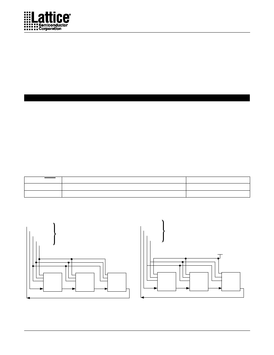
Data Path
Bus #1
Control
Inputs
(from
µ
P)
Address
Inputs
(from
µ
P)
Control
Outputs
System
Clock(s)
Data Path
Bus #2
Configuration
(Switch)
Outputs
ISP/JTAG
Interface
ispLSI Device
ispGDX Device
State Machines
Decoders
Buffers / Registers
Buffers / Registers
Figure 2. ispGDX Complements Lattice ispLSI
5
Specifications
ispGDX Family
Figure 4. Data Bus Byte Swapper
Figure 5. Four-Port Memory Interface
Designing with the ispGDX
As mentioned earlier, this architecture satisfies the PRSI
class of applications without restrictions: any I/O pin as a
single input or bidirectional can drive any other I/O pin as
output.
For the case of PDP applications, the designer does have
to take into consideration the limitations on pins that can
be used as control (MUX0, MUX1, OE, CLK) or data
(MUXA-D) inputs. The restrictions on control inputs are
not likely to cause any major design issues because the
input possibilities span 25% of the total pins.
The MUXA-D input partitioning requires that designers
consciously assign pinouts so that MUX inputs are in the
appropriate, disjoint groups. For example, since the
MUXA group includes I/O0-19 (80 I/O device), it is not
possible to use I/O0 and I/O9 in the same MUX function.
As previously discussed, data path functions will be
assigned early in the design process and these restric-
tions are reasonable in order to optimize speed and cost.
User Electronic Signature
The ispGDX Family includes dedicated User Electronic
Signature (UES) E
2
CMOS storage to allow users to code
design-specific information into the devices to identify
particular manufacturing dates, code revisions, or the
like. The UES information is accessible through the
boundary scan or Lattice ISP programming port via a
specific command. This information can be read even
when the security cell is programmed.
Security Bit
The ispGDX Family includes a security bit feature that
prevents reading the device program once set. Even
when set, it does not inhibit reading the UES or device ID
code. It can be erased only via a device bulk erase.
Applications (Cont.)
Contr
o
l Bus
Data Bus A
Data Bus B
OEA OEB
I/OA
D0-7
D8-15
D8-15
D0-7
I/OB
XCVR
OEA OEB
I/OA
I/OB
XCVR
OEA OEB
I/OA
I/OB
XCVR
OEA OEB
I/OA
I/OB
XCVR
Bus 4
Bus 3
Bus 2
Bus 1
Port #1
OE1
Memory
Port
OEM
SEL0
SEL1
To
Memory
Port #2
OE2
Port #3
OE3
Note: All OE and SEL lines driven by external arbiter logic (not shown).
Port #4
OE4
4-to-1
16-Bit MUX
Bidirectional
Figure 3. Address Demultiplex/Data Buffering
Contr
ol Bus
Mux
ed Ad
dress Data Bus
D
Q
CLK
OEA OEB
I/OA
I/OB
Address
Buffered
Data
To Memory/
Peripherals
XCVR
Address
Latch
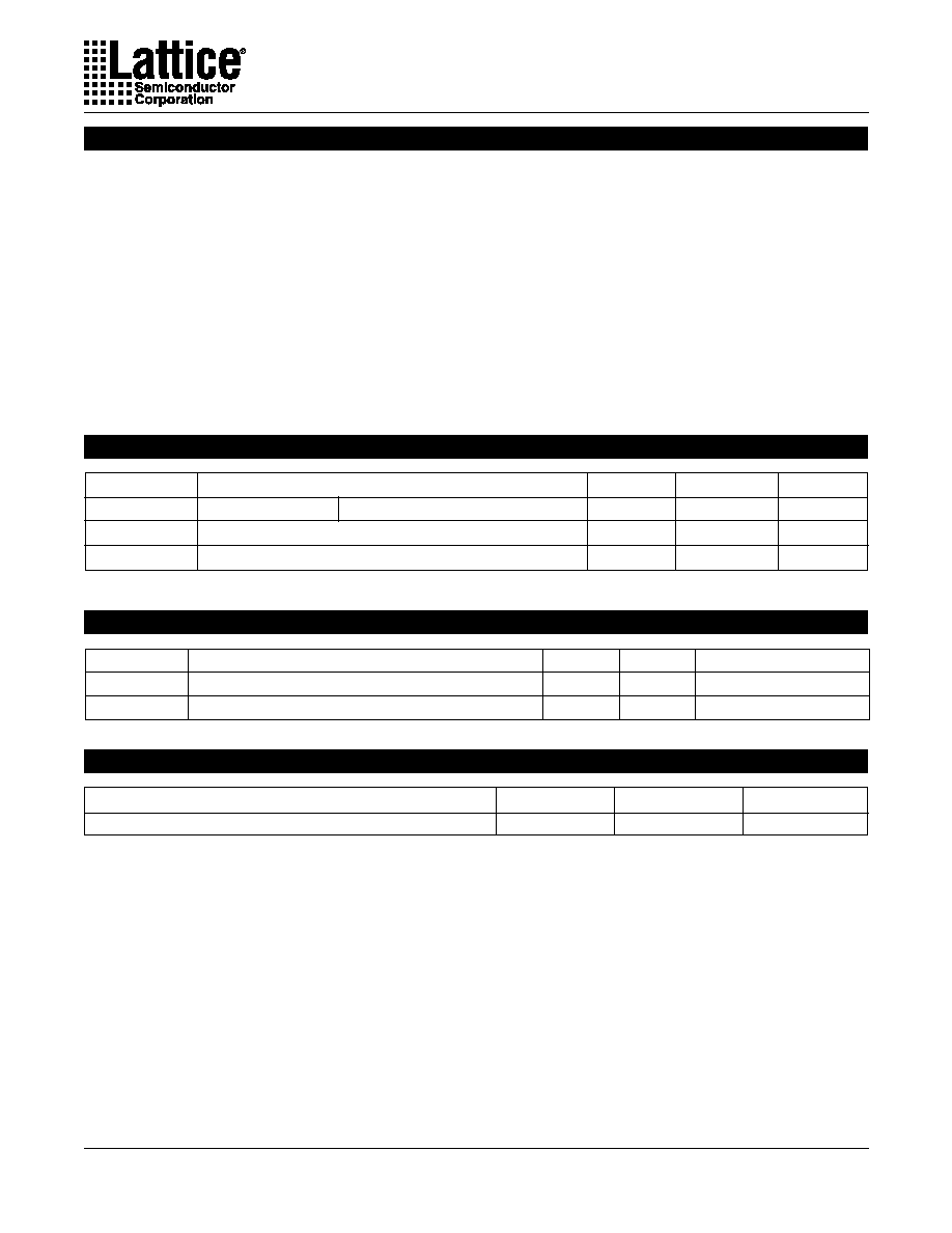
6
Specifications
ispGDX Family
Supply Voltage
Commercial T
A
=
0
∞
C to +70
∞
C
Input Low Voltage
Input High Voltage
5.25
0.8
Vcc + 1
Absolute Maximum Ratings
1
Supply Voltage V
cc
................................. -0.5 to +7.0V
Input Voltage Applied ........................ -2.5 to V
CC
+1.0V
Off-State Output Voltage Applied ..... -2.5 to V
CC
+1.0V
Storage Temperature ................................ -65 to 150
∞
C
Case Temp. with Power Applied .............. -55 to 125
∞
C
Max. Junction Temp. (T
J
) with Power Applied ... 150
∞
C
1. Stresses above those listed under the "Absolute Maximum Ratings" may cause permanent damage to the device. Functional
operation of the device at these or at any other conditions above those indicated in the operational sections of this specification
is not implied (while programming, follow the programming specifications).
DC Recommended Operating Conditions
V
V
V
PARAMETER
SYMBOL
MIN.
MAX.
UNITS
4.75
0
2.0
V
CC
V
IL
1
V
IH
1
1. Typical 100mV of input hysteresis.
C
SYMBOL
Table 2 - 0006
C
PARAMETER
Dedicated Clock Capacitance
10
UNITS
TYPICAL
TEST CONDITIONS
1
2
8
I/O Capacitance
pf
pf
V = 5.0V, V = 2.0V
V = 5.0V, V = 2.0V
CC
CC
Y
I/O
Capacitance (T
A
=25
o
C, f=1.0 MHz)
PARAMETER
MINIMUM
MAXIMUM
UNITS
ispGDX Erase/Reprogram Cycles
10,000
≠
Cycles
Erase/Reprogram Specifications
7
Specifications
ispGDX Family
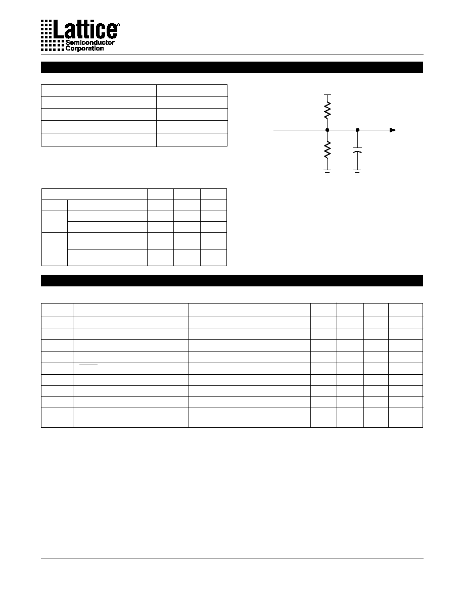
Switching Test Conditions
Output Load Conditions
TEST CONDITION
R1
R2
CL
A
160
90
35pF
B
90
35pF
160
90
35pF
Active High
Active Low
C
160
90
5pF
90
5pF
Active Low to Z
at V +0.5V
OL
Active High to Z
at V -0.5V
OH
Table 2 - 0004A
Output Low Voltage
Output High Voltage
Input or I/O Low Leakage Current
Input or I/O High Leakage Current
ispEN Input Low Leakage Current
I/O Active Pull-Up Current
Output Short Circuit Current
Quiescent Power Supply Current
Dynamic Power Supply Current
per Input Switching
V
V
µ
A
µ
A
µ
A
µ
A
mA
mA
mA/MHz
I
OL
=24 mA
I
OH
=-24 mA
0V
V
IN
V
IL
(MAX.)
3.5V
V
IN
V
CC
0V
V
IN
V
IL
(MAX.)
0V
V
IN
V
IL
V
CC
= 5V, V
OUT
= 0.5V, T
A
= 25∞C
V
IL
= 0.5V, V
IH
= V
CC
One input toggling @ 50% duty cycle,
outputs open.
V
OL
V
OH
I
IL
I
IH
I
IL-isp
I
IL-PU
I
OS
1
I
CCQ
I
CC
≠
≠
≠
≠
≠
≠
≠
25
See
Note 3
≠
2.4
≠
≠
≠
≠
-100
≠
≠
1. One output at a time for a maximum duration of one second. V
= 0.5V was selected to avoid test problems by tester ground
degradation. Characterized but not 100% tested.
2. Typical values are at V
= 5V and T
= 25
o
C.
3. I
/ MHz = (0.0114 x I/O cell fanout) + 0.06
e.g. An input driving four I/O cells at 40 MHz results in a dynamic I of approximately ((0.0114 x 4) + 0.06) x 40 = 4.2 mA.
SYMBOL
MIN.
MAX.
TYP.
2
PARAMETER
CONDITION
UNITS
0.55
≠
-10
10
-150
-150
-250
40
≠
Input Pulse Levels
GND to 3.0V
Input Rise and Fall Time
1.5ns 10% to 90%
Input Timing Reference Levels
1.5V
Output Timing Reference Levels
1.5V
Output Load
See figure at right
3-state levels are measured 0.5V from steady-state
active level.
CC
A
OUT
DC Electrical Characteristics
Over Recommended Operating Conditions
+ 5V
R1
R2
CL
*
Device
Output
Test
Point
*
CL includes Test Fixture and Probe Capacitance.
CC
CC
8
Specifications
ispGDX Family
External Timing Parameters
Over Recommended Operating Conditions
ns
ns
MHz
ns
ns
ns
ns
ns
ns
ns
ns
ns
ns
ns
ns
ns
ns
ns
ns
ns
≠
≠
111
4.0
4.0
0.0
≠
≠
≠
≠
≠
≠
≠
3.5
3.5
≠
10.0
≠
≠
5.0
6.5
≠
≠
≠
≠
5
8.5
6.0
9.5
6.0
6.0
9.0
9.0
≠
≠
14.0
≠
5.0
0.5
≠
≠
80.0
5.5
5.5
0.0
≠
≠
≠
≠
≠
≠
≠
5.0
5.0
≠
14.0
≠
≠
7.0
9.0
≠
≠
≠
≠
7.0
11.0
9.0
13.0
8.5
8.5
12.0
12.0
≠
≠
18.0
≠
7.0
0.5
1
2
3
4
5
6
7
8
9
10
11
12
13
14
15
16
17
18
19
20
A
A
≠
≠
≠
≠
A
A
A
A
B
C
B
C
≠
≠
≠
≠
A
A
Data Propagation Delay from any I/O pin to any I/O pin
Data Propagation Delay from MUXsel Inputs to any Output
Clock Frequency with External Feedback
Input Latch or Register Setup Time before any Clk
Output Latch or Register MUX Data Setup Time before any Clk
Latch or Register Hold Time after any Clk
Output Latch or Register Clk (from Y
x
) to Output Delay
Input Latch or Register Clk (from Y
x
) to Output Delay
Output Latch or Register Clk (from I/O pin) to Output Delay
Input Latch or Register Clock (from I/O pin) to Output Delay
Input to Output Enable
Input to Output Disable
Test OE Output Enable
Test OE Output Disable
Clock Pulse Duration, High
Clock Pulse Duration, Low
Register Reset Delay from RESET Low
Reset pulse width
Output Delay Adder for Output Timings Using Slow Slew Rate
Output Skew (tgco1 across chip)
t
pd
t
sel
f
max(ext)
t
su1
t
su2
t
h
t
gco1
t
gco2
t
co1
t
co2
t
en
t
dis
t
toeen
t
toedis
t
wh
t
wl
t
rst
t
rw
t
sl
t
sk
DESCRIPTION
PARAMETER
TEST
1
COND.
#
( )
1
tsu2+tgco1
UNITS
-5
MIN. MAX.
-7
MIN. MAX.
1. All timings measured with one output switching, fast output slew rate setting, except
t
sl
.
2
8
0
10
4
20
30
40
50
60
70
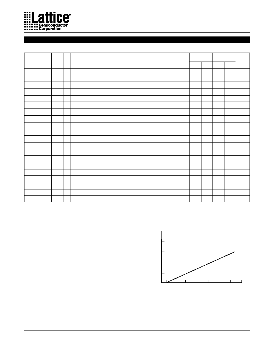
I/O Cell Fanout
GRP Delay (ns)
6
10
4
Maximum
GRP Delay vs. I/O Cell Fanout
ispGDX timings are specified with a GRP load (fanout) of
four I/O cells. The figure at right shows the Maximum
GRP Delay with increased GRP loads. These deltas
apply to any signal path traversing the GRP (MUXA-D,
OE, CLK, MUXsel0-1). Global Clock signals, which do
not use the GRP, have no fanout delay adder.
9
Specifications
ispGDX Family
-5
-7
PARAMETER #
2
DESCRIPTION
1
MIN. MAX. MIN. MAX. UNITS
Inputs
t
io
21 Input Buffer Delay
--
0.7
--
1.3
ns
GRP
t
grp
22 GRP Delay
--
2.0
--
2.5
ns
MUX
t
muxd
23 I/O Cell MUX A/B/C/D Data Delay
--
1.0
--
1.4
ns
t
muxs
24 I/O Cell MUX A/B/C/D Data Select
--
2.5
--
3.4
ns
Register
t
iolat
25 I/O Latch Delay
--
1.6
--
2.2
ns
t
iosu
26 I/O Register Setup Time Before Clock
--
1.6
--
1.8
ns
t
ioh
27 I/O Register Hold Time After Clock
--
2.4
--
3.6
ns
t
ioco
28 I/O Register Clock to Output Delay
--
1.6
--
2.2
ns
t
ior
29 I/O Reset to Output Delay
--
0.7
--
1.0
ns
Data Path
t
rfdbk
30 I/O Register Feedback Delay
--
0.2
--
0.3
ns
t
iobp
31 I/O Register Bypass Delay
--
0.4
--
0.6
ns
t
ioob
32 I/O Register Output Buffer Delay
--
0.1
--
0.7
ns
t
muxc
(Yx Clk) 33 I/O Register Data Input MUX Delay
--
1.1
--
1.2
ns
t
muxc
(I/O Clk) 34 I/O Register Data Input MUX Delay
--
2.1
--
3.2
ns
t
iod
(Yx Clk)
35 I/O Register I/O Input MUX Delay
--
4.1
--
5.1
ns
t
iod
(I/O Clk)
36 I/O Register I/O Input MUX Delay
--
5.1
--
7.1
ns
Outputs
t
ob
37 Output Buffer Delay
--
0.9
--
1.3
ns
t
obs
38 Output Buffer Delay, Slow Slew
--
5.9
--
8.3
ns
t
oen
39 I/O Cell OE to Output Enabled
--
0.8
--
1.1
ns
t
oedis
40 I/O Cell OE to Output Disabled
--
0.8
--
1.1
ns
t
goe
41 Global Output Enable Delay
--
2.5
--
3.6
ns
t
toe
42 Test OE Enable Delay
--
8.2
--
10.9
ns
Clocks
t
cio
43 I/O Clock Delay
--
0.7
--
1.0
ns
t
gy0/1/2/3
44 Clock Delay, Y0/1/2/3
--
2.4
--
2.8
ns
Global Reset
t
gr
45 Global Reset to I/O Register/Latch
--
12.3
--
15.0
ns
Internal Timing Parameters
1
Over Recommended Operating Conditions
1. Internal Timing Parameters are not tested and are for reference only.
2. Refer to the Timing Model in this data sheet for further details.
10
Specifications
ispGDX Family
ispGDX Timing Model
I/O Pin
Reset
TOE
Y0,1,2,3
tgy0/1/2/3 #44
MUX0
MUX1
tgrp #22
GRP
D
C
B
A
OE
tgoe #41
tiobp #31
tioob #32
tmuxd #23
tmuxs #24
tiod #35, #36
tgr #45
0902/gdx
tio #21
trfdbk #30
tmuxc #33, #34
tcio #43
tiolat #25
tiosu #26
tioh #27
tioco #28
tior #29
tob #37
tobs #38
toen #39
toedis #40
ttoe #42
Clock
D
Q
Switching Waveforms
Clock Width
CLK
(I/O INPUT)
t
wl
t
wh
COMBINATORIAL
I/O OUTPUT
VALID INPUT
DATA (I/O INPUT)
t
pd
t
sel
VALID INPUT
MUXSEL (I/O INPUT)
Combinatorial Output
COMBINATORIAL
I/O OUTPUT
OE (I/O INPUT)
t
en
t
dis
I/O Output Enable/Disable
DATA
(I/O INPUT)
REGISTERED
I/O OUTPUT
CLK
VALID INPUT
t
su1
t
co2
t
h
t
su2
t
co1
1/
f
max
(external fdbk)
t
gco1
t
gco2
Registered Output
Reset
REGISTERED
I/O OUTPUT
t
rst
RESET
t
rw
11
Specifications
ispGDX Family
ispGDX Development System
Lattice's ispGDX Development System Interface
The ispGDX Development System supports ispGDX
design using a simple language syntax and an easy-to-
use Graphical User Interface (GUI) called Design
Manager. From creation to In-System Programming, the
ispGDX system is an easy-to-use, self-contained design
tool delivered on CD-ROM media.
Features
∑ Easy-to-use Text Entry System
∑ ispGDX Design Compiler
- Design Rule Checker
- I/O Connectivity Checker
- Automatic Compiler Function
∑ Industry Standard JEDEC File for Programming
∑ Min / Max Timing Report
∑ Interfaces To Popular Timing Simulators
∑ User Electronic Signature (UES) Support
∑ Detailed Log and Report Files For Easy Design Debug
∑ On-Line Help
∑ Windows 3.1x, WIN95, and NT Compatible Graphical
User Interface
∑ SUN O/S, Command Line Driven version available
PC Version
With the ispGDX GUI for the PC, command line entry is
not required. The tools run under Microsoft Windows 3.1,
Windows 95 and Windows NT. When the ispGDX
software is invoked, the Design Manager and an accom-
panying message window are displayed. The Design
Manager consists of the Menu Bar, Tool Bar, Status Bar
and the work area. The figure below shows these
elements of the ispGDX GUI.
The Menu Bar displays topics related to functions used in
the design process. Access the various drop-down
menus and submenus by using the mouse or "hot" keys.
The menu items available in the ispGDX system are
FILE, EDIT, DEVICE, INVOKE, INTERFACES, VIEW,
WINDOW and HELP.
The Tool Bar is a quick and easy way to perform many of
the functions found in the menus with a single click of the
mouse. File, Edit, Undo, Redo, Find, Print Download and
Compiler are just some of the Icons found in the ispGDX
Tool Bar. For instance, the Compiler Icon performs the
same function as the Invoke => Compiler menu com-
mands, including design analysis and rule checking and
the fitting operation.
The Status Bar displays action prompts and the line and
column numbers reflect the location of the cursor within
the message window or the work area.
Workstation Version
The ispGDX software is also available for use under the
Sun O/S 4.1.x or Solaris 2.4 or 2.5. The Sun version of
the ispGDX software is invoked from the command line
under the UNIX operating system. A GUI is not sup-
ported in this environment.
In the UNIX environment, the ispGDX Design File (GDF)
must be created using a text editor. Once the GDF has
been created, invoke the ispGDX workstation software
from the UNIX command line. The following is an ex-
ample of how to invoke ispGDX software.
Usage:
ispGDX
[-i input_file]
[-of[edif|orcad|viewlogic|verilog|vhdl]]
[-p part name]
[-r par_file]
-i input_file name
ispGDX design file
-of [edif | orcad | viewlogic | verilog | vhdl]
output format
-p part_name
ispGDX part number
-r par_file
read parameters from parameter file
12
Specifications
ispGDX Family
The GDF File
The GDF file is a simple text description of the design
function, device and pin parameters. The file has four
parts: device selection, set and constant statements, a
pin section and a connection section. A sample file looks
like this:
//32-bit data exchange from A-bus to B-bus
DESIGN a2bexch
PART ispGDX160-5Q208;
PARAM SECURITY ON;
PARAM PULLUP OFF;
SET busA [dataA0..dataA31];
SET busB [dataB0..dataB31];
BIDI busA {A0..A31} PULLUP SLOWSLEW;
BIDI busB {B0..B31} PULLUP SLOWSLEW;
INPUT [oe0] {C1};
BEGIN
busA.oe = oe0;
busB.oe = !oe0;
busA.m1 = busB;
busA.s0 = VCC;
busA.s1 = GND;
busB.m0 = busA;
busB.s0 = GND;
busB.s1 = GND;
END
This example shows a simple, but complete, 32-bit A-bus
to B-bus data exchange design. Once completed, the
compiler takes over.
Powerful Syntax
Lattice's ispGDX Design System uses simple, but power-
ful, syntax to easily define a design. The !(bang) operator
controls pin polarity and can be used in both the pin and
connection sections of the design definition. Dot exten-
sions define data inputs, select controls for the 4:1
multiplexor, and control inputs of sequential elements
and tri-state buffers. Dot extensions are .M# (MUX
Input), .S# (MUX Select), and control functions, such as
.CLK, .EN, .OE (shown in adjacent table). Pin Attributes
are assigned in the pin section of the GDF as well.
SLOWSLEW selects the slow slew rate for an output
buffer. PULLUP fixes the on-chip pullup resistor for a
particular pin. The COMB attribute distinguishes the
structure for bidirectional pins. If COMB is used, the input
register, or latch, of an output buffer will be applied to
bidirectional pins.
Please consult the ispGDX Development System Manual
for full details.
The ispGDX Design System Compiler
After the GDF file is created, the compiler checks the
syntax and provides helpful hints and the location of any
syntax errors. The compiler performs design rule checks,
such as, clock and enable designations, the use of input/
output/BIDI usage, and the proper use of attributes. I/O
connectivity is also checked to ensure polarity, MUX
selection controls, and connections are properly made.
Compilation is completed automatically and report and
programming files are saved.
Reports Generated
When the ispGDX system compiles a design and gener-
ates the specified netlists, the following output files are
created:
Report Files
.log - Compiler History
.rpt
- Compiler Report
.rt1
- Minimum Delay Timing Report
.rt2
- Maximum Delay Timing Report
Simulation File
.sim -
Post-Route Simulation With LAC Format
Netlists
.edo - EDIF Output
.vlo - Verilog Output
.edo - Viewlogic EDIF-format Output
.ifo
- OrCAD Output
.vho - VHDL non-VITAL with Maximum Delays Output
.vhn - VHDL non-VITAL with Maximum Delays Output
.vto - VHDL VITAL Output
TYPE
DOT EXT.
DESCRIPTION
MUX
Input
MUX
Selection
Control
.M0
MUXA Data input to 4-1 MUX
.M1
MUXB Data input to 4-1 MUX
MUX0 Selection input to 4-1 MUX
MUX1 Selection input to 4-1 MUX
.M2
MUXC Data Input to 4-1 MUX
.M3
.S0
.S1
MUXD Data Input to 4-1 MUX
.CLK
Clock for a register signal
.EN
Latch enable for a latch signal
.OE
Output enable for 3-state output
or bidirectional signal
ispGDX Dot Ext
ispGDX GDF File Dot Extensions
13
Specifications
ispGDX Family
Download
.jed - JEDEC Device Programming File
Third-Party Timing Simulation
The ispGDX Design System will generate simulation
netlists as specified by a user. The simulation netlist
formats available are: EDIF, Verilog (OVI compliant),
VHDL (VITAL compliant), Viewlogic, and OrCAD.
For In-System Programming, Lattice's ispGDX devices
may be programmed, alone or in a chain with up to 100
other Lattice ISP devices, using Lattice's ISP Daisy
Chain Download software. This powerful Windows-
based tool can be launched from the Tool Bar or by
Invoking the Download option from the drop down menu
within the ispGDX Design System. ISP Daisy Chain
Download version 5.0 or above supports the ispGDX
Family devices.
Figure 5. ISP Device Programming Interface
ispGDX
80A
SDO
SDI
MODE
SCLK
ispEN
5-wire
Programming
Interface
ispGDX
120A
ispGDX
160/A
BSCAN/
ispEN
BSCAN/
ispEN
BSCAN/
ispEN
Figure 6. ispJTAG Device Programming Interface
ispGDX
80A
TDO
TDI
TMS
TCK
ispJTAG
Programming
Interface
ispGDX
120A
ispGDX
160/A
BSCAN/
ispEN
BSCAN/
ispEN
BSCAN/
ispEN
VCC
In-System Programmability
All necessary programming of the ispGDX Family is done
via five TTL level logic interface signals. These five
signals are fed into the on-chip programming circuitry
where a state machine controls the programming.
On-chip programming can be accomplished using either
an IEEE 1149.1 boundary scan protocol or a Lattice
industry-standard ISP programming protocol. The IEEE
1149.1-compliant interface signals are Test Data In (TDI),
Test Data Out (TDO), Test Clock (TCK) and Test Mode
Select (TMS) control. The corresponding Lattice ISP
control signals are SDI, SDO, SCLK and MODE. These
signals switch their operation from IEEE 1149.1 bound-
ary scan protocol to Lattice ISP programming protocol
based on the state of the BSCAN/
ispEN
pin as shown in
Table 2. Figure 5 illustrates the block diagram for the ISP
programming interface. Figure 6 illustrates the block
diagram for the ispJTAG interface.
Table 2. Operating Mode Control Signals
Op Mode Signals/ispGDX
SDI, SDO, SCLK, MODE
0
Program Device Using Lattice ISP Protocol
TDI, TDO, TCK, TMS
1
Program Device or Normal Operation Using IEEE 1149.1 Protocol
BSCAN/ispEN
OPERATION
CONTROL PIN FUNCTION
14
Specifications
ispGDX Family
Boundary Scan / ISP Programming and Test Options
The ispGDX devices provide IEEE1149.1a test capabil-
ity and ISP programming through a standard Boundary
Scan Test Access Port (TAP) interface. In addition,
ispGDX devices can be programmed via the Lattice ISP
programming interface using the same TAP serial inter-
face pins.
When the BSCAN/
ispEN
signal is high the ispGDX de-
vices enable Boundary Scan Test mode. Under this
mode the Boundary Scan data registers for the I/O pins
are organized in the order given below. Each
I/O register is structured as shown in Figure 7.
The operation of the boundary scan test circuitry in the
ispGDX160 is dependent on the fuse pattern programmed
into the device. The boundary scan circuitry on the
ispGDX160A, ispGDX120A and ispGDX80A operates
independently of the programmed pattern. This allows
customers using boundary scan test to have full test
capability with only a single BSDL file.
Table 3. I/O Shift Register Order
Figure 7. Boundary Scan I/O Register Cell
D
Q
M
U
X
D
Q
D
Q
D
Q
D
Q
M
U
X
M
U
X
M
U
X
M
U
X
Normal
Function
OE
I/O Pin
EXTEST
Update DR
SCANOUT (to next cell)
Clock DR
SCANIN
(from
previous
cell)
Shift DR
Normal
Function
OE
TOE
I/O Shift Reg Order/ispGDX
ispGDX80A
SDI/TDI, I/O B10 .. B19, I/O C0 .. C19, I/O D0 .. D9,
RESET
, Y1/TOE, Y0, I/O B9 .. B0, I/O A19.. A0,
I/O D19 .. D10, SDO/TDO
ispGDX120A
SDI/TDI, I/O B15 .. B29, I/O C0 .. C29, I/O D0 .. D14, TOE, Y2, Y3,
RESET
, Y1, Y0, I/O B14 .. B0,
I/O A29.. A0, I/O D29 .. D15, SDO/TDO
ispGDX160/A
SDI/TDI, I/O B20 .. B39, I/O C0 .. C39, I/O D0 .. D19, TOE, Y2, Y3,
RESET
, Y1, Y0, I/O B19 .. B0,
I/O A39.. A0, I/O D39 .. D20, SDO/TDO
I/O SHIFT REGISTER ORDER
DEVICE

15
Specifications
ispGDX Family
The ispGDX devices are identified either by the 32-bit
JTAG IDCODE register or the eight-bit ISP register. The
device ID assignments are listed in Table 4.
The ispJTAG programming is accomplished by execut-
ing Lattice private instructions under the Boundary Scan
State Machine.
Lattice ISP programming is accomplished by driving
BSCAN/
ispEN
low, while following the ISP state machine
1
0
0
1
1
0
0
1
0
0
0
0
1
0
1
1
0
1
0
1
1
1
0
1
0
0
1
1
1
0
0
1
Update-IR
Exit2-IR
Pause-IR
Exit1-IR
Shift-IR
Capture-IR
Select-IR-Scan
Update-DR
Exit2-DR
Pause-DR
Exit1-DR
Shift-DR
Capture-DR
Select-DR-Scan
Run-Test/Idle
Test-Logic-Reset
TCK
TMS or
TDI
TDO
tsu
th
tco
tsu = 0.1
µ
s (min.) th = 0.1
µ
s (min.) tco = 0.1
µ
s (min.)
Figure 8. Boundary Scan State Machine
Boundary Scan / ISP Programming and Test Options (Continued)
algorithm. The eight-bit device ID can be read from the
device in Idle State for ISP device identification. Details
of the programming sequence are transparent to the user
and are handled by Lattice ISP Daisy Chain Downlowad
(ispDCD), ispCODE `C' routines or any third-party pro-
grammers. Contact Lattice Technical Support to obtain
more detailed programming information.
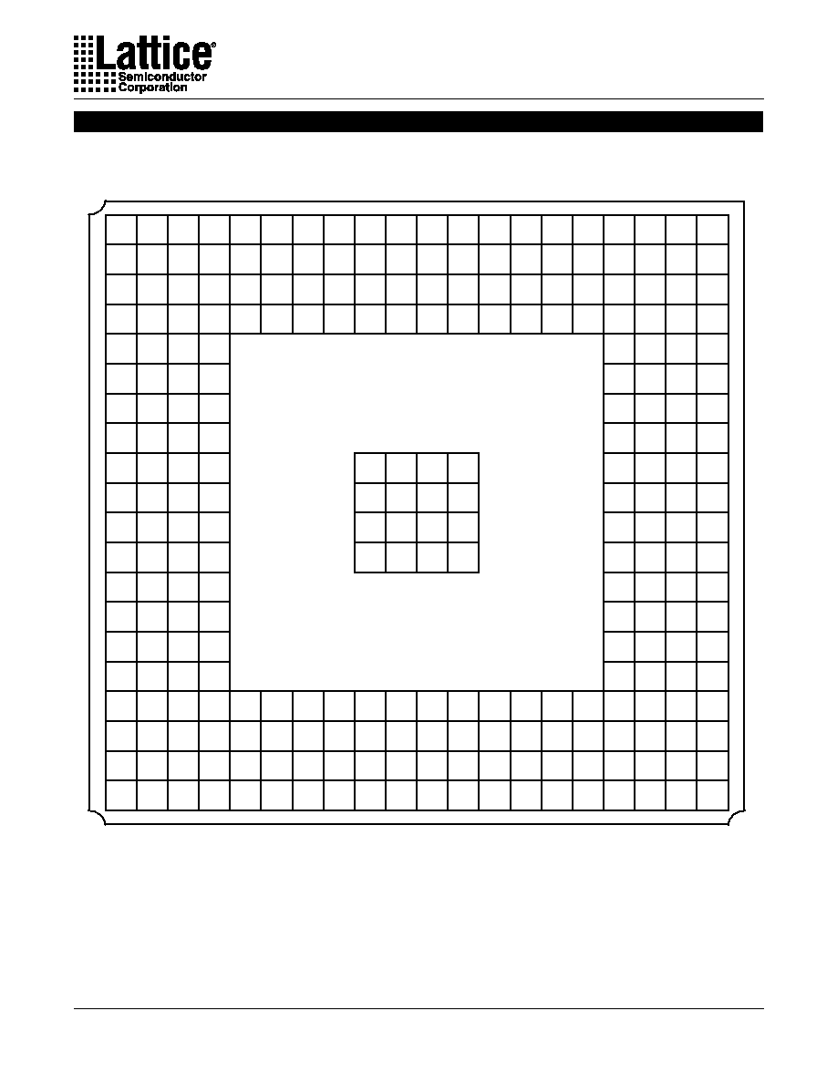
Table 4. ispGDX Device ID Codes
GDX ID Codes
0000 0000 0010 0101 0001 0000 0100 0011
0000 0000 0010 0101 0011 0000 0100 0011
ispGDX80A
ispGDX160/A
0111 0111
0000 0000 0010 0101 0010 0000 0100 0011
ispGDX120A
0111 1000
0111 1001
8-BIT ISP ID
32-BIT BOUNDARY SCAN IDCODE
DEVICE
16
Specifications
ispGDX Family
TOE
178
A12
RESET
185
D10
Y0, Y1, Y2, Y3, 75, 76, 180, 181
V10, Y10, C11, A11
BSCAN/
ispEN
183
B10
TDI/SDI
81
Y12
TCK/SCLK
80
U11
TMS/MODE
79
V11
TDO/SDO
78
W11
GND
6, 15, 25, 35, 44, 54, 63, 77, 91, 100, 110, 119, 129, A1, D4, D8, D13, D17, H4, H17, J9, J10, J11, J12,
139, 148, 159, 168, 182, 195, 204
K9, K10, K11, K12, L9, L10, L11, L12, M9, M10,
M11, M12, N4, N17, U4, U8, U13, U17
VCC
1, 17, 33, 49, 65, 89, 105, 121, 137, 153, 170, 184
D6, D11, D15, F4, F17, K4, L17, R4, R17, U6, U10,
193
U15
NC
1
73, 74, 156, 179
A2, A6, A7, A10, A15, A19, A20, B1, B2, B4, B11,
B14, B18, B19, B20, C2, C3, C10, C18, D2, D3, D16,
E2, E17, E19, H1, H3, H18, H20, K20, L1, N1, N3,
N18, N20, T2, T4, T19, U5, U18, U19, V3, V14, V18,
V19, W1, W2, W3, W7, W10, W14, W19, W20, Y1,
Y2, Y6, Y9, Y11, Y18, Y20
Signal Descriptions
I/O
Input/Output Pins ≠ These are the general purpose bidirectional data pins. When used as outputs, each
may be independently latched, registered or tristated. They can also each assume one other control
function (OE, CLK and MUXsel as described in the text).
TOE
Test Output Enable pin ≠ This pin tristates all I/O pins when a logic low is driven.
RESET
Active LOW Input Pin ≠ Resets all I/O register outputs when LOW.
Y0, Y1, Y2, Y3
Input Pins ≠ Dedicated clock input pins. Each pin can drive any or all I/O cell registers.
BSCAN/
ispEN
Input Pin ≠ When HIGH, this pin enables the Boundary Scan Test and Programming Interface. When
LOW, this pin enables the Lattice ISP protocol for programming and tristates all I/O pins, except those
used for the programming interface.
TDI/SDI
Input/Input Pin ≠ Serial data input during ISP programming or Boundary Scan mode.
TCK/SCLK
Input/Input Pin ≠ Serial data clock during ISP programming or Boundary Scan mode.
TMS/MODE
Input/Input Pin ≠ Control input during ISP programming or Boundary Scan mode.
TDO/SDO
Output/Output Pin ≠ Serial data output during ISP programming or Boundary Scan mode.
GND
Ground (GND)
VCC
Vcc ≠ Supply voltage (5V).
NC
1
No Connect.
Signal Name Description
1. NC pins are not to be connected to any active signals, VCC or GND.
Signal 208-Pin PQFP 272-Ball BGA
1. NC pins are not to be connected to any active signals, VCC or GND.
Signal Locations: ispGDX160/A

17
Specifications
ispGDX Family
I/O Locations: ispGDX160/A
I/O A0
2
E4
I/O A1
3
C1
I/O A2
4
D1
I/O A3
5
E3
I/O A4
7
E1
I/O A5
8
F3
I/O A6
9
G4
I/O A7
10
F2
I/O A8
11
F1
I/O A9
12
G3
I/O A10
13
G2
I/O A11
14
G1
I/O A12
16
H2
I/O A13
18
J4
I/O A14
19
J3
I/O A15
20
J2
I/O A16
21
J1
I/O A17
22
K2
I/O A18
23
K3
I/O A19
24
K1
I/O A20
26
L2
I/O A21
27
L3
I/O A22
28
L4
I/O A23
29
M1
I/O A24
30
M2
I/O A25
31
M3
I/O A26
32
M4
I/O A27
34
N2
I/O A28
36
P1
I/O A29
37
P2
I/O A30
38
R1
I/O A31
39
P3
I/O A32
40
R2
I/O A33
41
T1
I/O A34
42
P4
I/O A35
43
R3
I/O A36
45
U1
I/O A37
46
T3
I/O A38
47
U2
I/O A39
48
V1
I/O B0
50
U3
I/O B1
51
V2
I/O B2
52
W4
I/O B3
53
V4
I/O B4
55
Y3
I/O B5
56
Y4
I/O B6
57
V5
I/O B7
58
W5
I/O B8
59
Y5
I/O B9
60
V6
I/O B10
61
U7
I/O B11
62
W6
I/O B12
64
V7
I/O B13
66
Y7
I/O B14
67
V8
I/O B15
68
W8
I/O B16
69
Y8
I/O B17
70
U9
I/O B18
71
V9
I/O B19
72
W9
I/O B20
82
W12
I/O B21
83
V12
I/O B22
84
U12
I/O B23
85
Y13
I/O B24
86
W13
I/O B25
87
V13
I/O B26
88
Y14
I/O B27
90
Y15
I/O B28
92
W15
I/O B29
93
Y16
I/O B30
94
U14
I/O B31
95
V15
I/O B32
96
W16
I/O B33
97
Y17
I/O B34
98
V16
I/O B35
99
W17
I/O B36
101
U16
I/O B37
102
V17
I/O B38
103
W18
I/O B39
104
Y19
I/O C0
106
T17
I/O C1
107
V20
I/O C2
108
U20
I/O C3
109
T18
I/O C4
111
T20
I/O C5
112
R18
I/O C6
113
P17
I/O C7
114
R19
I/O C8
115
R20
I/O C9
116
P18
I/O C10
117
P19
I/O C11
118
P20
I/O C12
120
N19
I/O C13
122
M17
I/O C14
123
M18
I/O C15
124
M19
I/O C16
125
M20
I/O C17
126
L19
I/O C18
127
L18
I/O C19
128
L20
I/O C20
130
K19
I/O C21
131
K18
I/O C22
132
K17
I/O C23
133
J20
I/O C24
134
J19
I/O C25
135
J18
I/O C26
136
J17
I/O C27
138
H19
I/O C28
140
G20
I/O C29
141
G19
I/O C30
142
F20
I/O C31
143
G18
I/O C32
144
F19
I/O C33
145
E20
I/O C34
146
G17
I/O C35
147
F18
I/O C36
149
D20
I/O C37
150
E18
I/O C38
151
D19
I/O C39
152
C20
I/O D0
154
D18
I/O D1
155
C19
I/O D2
157
B17
I/O D3
158
C17
I/O D4
160
A18
I/O D5
161
A17
I/O D6
162
C16
I/O D7
163
B16
I/O D8
164
A16
I/O D9
165
C15
I/O D10
166
D14
I/O D11
167
B15
I/O D12
169
C14
I/O D13
171
A14
I/O D14
172
C13
I/O D15
173
B13
I/O D16
174
A13
I/O D17
175
D12
I/O D18
176
C12
I/O D19
177
B12
I/O D20
186
A9
I/O D21
187
B9
I/O D22
188
C9
I/O D23
189
D9
I/O D24
190
A8
I/O D25
191
B8
I/O D26
192
C8
I/O D27
194
B7
I/O D28
196
C7
I/O D29
197
B6
I/O D30
198
A5
I/O D31
199
D7
I/O D32
200
C6
I/O D33
201
B5
I/O D34
202
A4
I/O D35
203
C5
I/O D36
205
A3
I/O D37
206
D5
I/O D38
207
C4
I/O D39
208
B3
208
272
Signal
PQFP BGA
208
272
Signal
PQFP BGA
208
272
Signal
PQFP
BGA
208
272
Signal
PQFP
BGA
208
272
Signal
PQFP
BGA
18
Specifications
ispGDX Family
Signal Configuration: ispGDX160/A
ispGDX160/A 272-Ball BGA Signal Diagram
20
19
18
17
16
15
14
13
12
11
10
9
8
7
6
5
4
3
2
1
A
NC
1
NC
1
I/O
D4
I/O
D5
I/O
D8
NC
1
I/O
D13
I/O
D16
TOE
Y3
NC
1
I/O
D20
I/O
D24
NC
1
NC
1
I/O
D30
I/O
D34
I/O
D36
NC
1
GND
A
B
NC
1
NC
1
NC
1
I/O
D2
I/O
D7
I/O
D11
NC
1
I/O
D15
I/O
D19
NC
1
BSCAN/
ispEN
I/O
D21
I/O
D25
I/O
D27
I/O
D29
I/O
D33
NC
1
I/O
D39
NC
1
NC
1
B
C
I/O
C39
I/O
D1
NC
1
I/O
D3
I/O
D6
I/O
D9
I/O
D12
I/O
D14
I/O
D18
Y2
NC
1
I/O
D22
I/O
D26
I/O
D28
I/O
D32
I/O
D35
I/O
D38
NC
1
NC
1
I/O
A1
C
D
I/O
C36
I/O
C38
I/O
D0
GND NC
1
VCC
I/O
D10
GND
I/O
D17
VCC
RESET
I/O
D23
GND
I/O
D31
VCC
I/O
D37
GND NC
1
NC
1
I/O
A2
D
E
I/O
C33
NC
1
I/O
C37
NC
1
I/O
A0
I/O
A3
NC
1
I/O
A4
E
F
I/O
C30
I/O
C32
I/O
C35
VCC
ispGDX160/A
VCC
I/O
A5
I/O
A7
I/O
A8
F
G
I/O
C28
I/O
C29
I/O
C31
I/O
C34
Bottom View
I/O
A6
I/O
A9
I/O
A10
I/O
A11
G
H
NC
1
I/O
C27
NC
1
GND
GND NC
1
I/O
A12
NC
1
H
J
I/O
C23
I/O
C24
I/O
C25
I/O
C26
GND GND GND GND
I/O
A13
I/O
A14
I/O
A15
I/O
A16
J
K
NC
1
I/O
C20
I/O
C21
I/O
C22
GND GND GND GND
VCC
I/O
A18
I/O
A17
I/O
A19
K
L
I/O
C19
I/O
C17
I/O
C18
VCC
GND GND GND GND
I/O
A22
I/O
A21
I/O
A20
NC
1
L
M
I/O
C16
I/O
C15
I/O
C14
I/O
C13
GND GND GND GND
I/O
A26
I/O
A25
I/O
A24
I/O
A23
M
N
NC
1
I/O
C12
NC
1
GND
GND NC
1
I/O
A27
NC
1
N
P
I/O
C11
I/O
C10
I/O
C9
I/O
C6
I/O
A34
I/O
A31
I/O
A29
I/O
A28
P
R
I/O
C8
I/O
C7
I/O
C5
VCC
VCC
I/O
A35
I/O
A32
I/O
A30
R
T
I/O
C4
NC
1
I/O
C3
I/O
C0
NC
1
I/O
A37
NC
1
I/O
A33
T
U
I/O
C2
NC
1
NC
1
GND
I/O
B36
VCC
I/O
B30
GND
I/O
B22
TCK/
SCLK
VCC
I/O
B17
GND
I/O
B10
VCC NC
1
GND
I/O
B0
I/O
A38
I/O
A36
U
V
I/O
C1
NC
1
NC
1
I/O
B37
I/O
B34
I/O
B31
NC
1
I/O
B25
I/O
B21
TMS/
MODE
Y0
I/O
B18
I/O
B14
I/O
B12
I/O
B9
I/O
B6
I/O
B3
NC
1
I/O
B1
I/O
A39
V
W
NC
1
NC
1
I/O
B38
I/O
B35
I/O
B32
I/O
B28
NC
1
I/O
B24
I/O
B20
TDO/
SDO
NC
1
I/O
B19
I/O
B15
NC
1
I/O
B11
I/O
B7
I/O
B2
NC
1
NC
1
NC
1
W
Y
NC
1
I/O
B39
NC
1
I/O
B33
I/O
B29
I/O
B27
I/O
B26
I/O
B23
TDI/
SDI
NC
1
Y1
NC
1
I/O
B16
I/O
B13
NC
1
I/O
B8
I/O
B5
I/O
B4
NC
1
NC
1
Y
20
19
18
17
16
15
14
13
12
11
10
9
8
7
6
5
4
3
2
1
1. NCs are not to be connected to any active signals, Vcc or GND.
Note: Ball A1 indicator dot on top side of package.

19
Specifications
ispGDX Family
Pin Configuration: ispGDX160/A
ispGDX160/A 208-Pin PQFP (with Heat Spreader) Pinout Diagram
ispGDX160/A
Top View
1
2
3
4
5
6
7
8
9
10
11
12
13
14
15
16
17
18
19
20
21
22
23
24
25
26
27
28
29
30
31
32
33
34
35
36
37
38
39
40
41
42
43
44
45
46
47
48
49
50
51
52
53
54
55
56
57
58
59
60
61
62
63
64
65
66
67
68
69
70
71
72
73
74
75
76
77
78
79
80
81
82
83
84
85
86
87
88
89
90
91
92
93
94
95
96
97
98
99
100
101
102
103
104
156
155
154
153
152
151
150
149
148
147
146
145
144
143
142
141
140
139
138
137
136
135
134
133
132
131
130
129
128
127
126
125
124
123
122
121
120
119
118
117
116
115
114
113
112
111
110
109
108
107
106
105
208
207
206
205
204
203
202
201
200
199
198
197
196
195
194
193
192
191
190
189
188
187
186
185
184
183
182
181
180
179
178
177
176
175
174
173
172
171
170
169
168
167
166
165
164
163
162
161
160
159
158
157
VCC
I/O A 0
I/O A 1
I/O A 2
I/O A 3
GND
I/O A 4
I/O A 5
I/O A 6
I/O A 7
I/O A 8
I/O A 9
I/O A 10
I/O A 11
GND
I/O A 12
VCC
I/O A 13
I/O A 14
I/O A 15
I/O A 16
I/O A 17
I/O A 18
I/O A 19
GND
I/O A 20
I/O A 21
I/O A 22
I/O A 23
I/O A 24
I/O A 25
I/O A 26
VCC
I/O A 27
GND
I/O A 28
I/O A 29
I/O A 30
I/O A 31
I/O A 32
I/O A 33
I/O A 34
I/O A 35
GND
I/O A 36
I/O A 37
I/O A 38
I/O A 39
VCC
I/O B 0
I/O B 1
I/O B 2
--
CLK
OE
MUXsel1
MUXsel2
--
CLK
OE
MUXsel1
MUXsel2
CLK
OE
MUXsel1
MUXsel2
--
CLK
--
OE
MUXsel1
MUXsel2
CLK
OE
MUXsel1
MUXsel2
--
CLK
OE
MUXsel1
MUXsel2
CLK
OE
MUXsel1
--
MUXsel2
--
CLK
OE
MUXsel1
MUXsel2
CLK
OE
MUXsel1
MUXsel2
--
CLK
OE
MUXsel1
MUXsel2
--
CLK
OE
MUXsel1
NC
1
I/O D1
I/O D 0
VCC
I/O C 39
I/O C 38
I/O C 37
I/O C 36
GND
I/O C 35
I/O C 34
I/O C 33
I/O C 32
I/O C 31
I/O C 30
I/O C 29
I/O C 28
GND
I/O C 27
VCC
I/O C 26
I/O C 25
I/O C 24
I/O C 23
I/O C 22
I/O C 21
I/O C 20
GND
I/O C 19
I/O C 18
I/O C 17
I/O C 16
I/O C 15
I/O C 14
I/O C 13
VCC
I/O C 12
GND
I/O C 11
I/O C 10
I/O C 9
I/O C 8
I/O C 7
I/O C 6
I/O C 5
I/O C 4
GND
I/O C 3
I/O C 2
I/O C 1
I/O C 0
VCC
Data
Control
MUXsel2
--
CLK
OE
MUXsel1
MUXsel2
CLK
OE
MUXsel1
MUXsel2
--
CLK
--
OE
MUXsel1
MUXsel2
CLK
OE
MUXsel1
MUXsel2
--
--
--
--
--
--
--
--
--
CLK
OE
MUXsel1
MUXsel2
CLK
OE
MUXsel1
--
MUXsel2
--
CLK
OE
MUXsel1
MUXsel2
CLK
OE
MUXsel1
MUXsel2
--
CLK
OE
MUXsel1
MUXsel2
Data
Control
I/O B 3
GND
I/O B 4
I/O B 5
I/O B 6
I/O B 7
I/O B 8
I/O B 9
I/O B 10
I/O B 11
GND
I/O B 12
VCC
I/O B 13
I/O B 14
I/O B 15
I/O B 16
I/O B 17
I/O B 18
I/O B 19
1
NC
1
NC
Y0
Y1
GND
TDO/SDO
TMS/MODE
TCK/SCLK
TDI/SDI
I/O B 20
I/O B 21
I/O B 22
I/O B 23
I/O B 24
I/O B 25
I/O B 26
VCC
I/O B 27
GND
I/O B 28
I/O B 29
I/O B 30
I/O B 31
I/O B 32
I/O B 33
I/O B 34
I/O B 35
GND
I/O B 36
I/O B 37
I/O B 38
I/O B 39
--
OE
CLK
--
MUXsel2
MUXsel1
OE
CLK
--
MUXsel2
MUXsel1
OE
CLK
MUXsel2
MUXsel1
OE
CLK
--
MUXsel2
--
MUXsel1
OE
CLK
MUXsel2
MUXsel1
OE
CLK
--
MUXsel2
MUXsel1
OE
CLK
MUXsel2
MUXsel1
OE
--
CLK
--
MUXsel2
MUXsel1
OE
CLK
MUXsel2
MUXsel1
OE
CLK
--
MUXsel2
MUXsel1
OE
CLK
--
Data
Control
I/O D 39
I/O D 38
I/O D 37
I/O D 36
GND
I/O D 35
I/O D 34
I/O D 33
I/O D 32
I/O D 31
I/O D 30
I/O D 29
I/O D 28
GND
I/O D 27
VCC
I/O D 26
I/O D 25
I/O D 24
I/O D 23
I/O D 22
I/O D 21
I/O D 20
RESET
VCC
BSCAN/ispEN
GND
Y3
Y2
NC
1
TOE
I/O D 19
I/O D 18
I/O D 17
I/O D 16
I/O D 15
I/O D 14
I/O D 13
VCC
I/O D 12
GND
I/O D 11
I/O D 10
I/O D 9
I/O D 8
I/O D 7
I/O D 6
I/O D 5
I/O D 4
GND
I/O D 3
I/O D 2
MUXsel2
MUXsel1
OE
CLK
--
MUXsel2
MUXsel1
OE
CLK
MUXsel2
MUXsel1
OE
CLK
--
MUXsel2
--
MUXsel1
OE
CLK
MUXsel2
MUXsel1
OE
CLK
--
--
--
--
--
--
--
--
MUXsel2
MUXsel1
OE
CLK
MUXsel2
MUXsel1
OE
--
CLK
--
MUXsel2
MUXsel1
OE
CLK
MUXsel2
MUXsel1
OE
CLK
--
MUXsel2
MUXsel1
Data
Control
1. No Connect Pins (NC) are not to be connected to any active signal, Vcc or GND.
20
Specifications
ispGDX Family
Signal Locations: ispGDX120A
TOE
150
136
RESET
156
142
Y0, Y1, Y2, Y3, 63, 64, 152, 153
57, 58, 138, 139
BSCAN/
ispEN
154
140
TDI/SDI
69
63
TCK/SCLK
68
62
TMS/MODE
67
61
TDO/SDO
66
60
GND
8, 17, 27, 37, 50, 65, 77, 91, 101, 110, 120, 129,
6, 15, 25, 35, 44, 59, 71, 81, 91, 100, 110, 119, 130,
144, 161, 170
147, 156
VCC
3, 19, 35, 55, 79, 99, 115, 136, 155, 159
1, 17, 33, 49, 73, 89, 105, 122, 141, 145
NC
1
1, 2, 43, 44, 45, 46, 61, 62, 87, 88, 89, 90, 130, 131, 55, 56, 120, 137
132, 133, 134, 151, 175, 176
Signal 176-Pin TQFP 160-Pin PQFP
1. NC pins are not to be connected to any active signals, VCC or GND.
I/O Locations: ispGDX120A
176
160
Signal
TQFP PQFP
I/O A0
4
2
I/O A1
5
3
I/O A2
6
4
I/O A3
7
5
I/O A4
9
7
I/O A5
10
8
I/O A6
11
9
I/O A7
12
10
I/O A8
13
11
I/O A9
14
12
I/O A10
15
13
I/O A11
16
14
I/O A12
18
16
I/O A13
20
18
I/O A14
21
19
I/O A15
22
20
I/O A16
23
21
I/O A17
24
22
I/O A18
25
23
I/O A19
26
24
I/O A20
28
26
I/O A21
29
27
I/O A22
30
28
I/O A23
31
29
I/O A24
32
30
I/O A25
33
31
I/O A26
34
32
I/O A27
36
34
I/O A28
38
36
I/O A29
39
37
I/O B0
40
38
I/O B1
41
39
I/O B2
42
40
I/O B3
47
41
I/O B4
48
42
I/O B5
49
43
I/O B6
51
45
I/O B7
52
46
I/O B8
53
47
I/O B9
54
48
I/O B10
56
50
I/O B11
57
51
I/O B12
58
52
I/O B13
59
53
I/O B14
60
54
I/O B15
70
64
I/O B16
71
65
I/O B17
72
66
I/O B18
73
67
I/O B19
74
68
I/O B20
75
69
I/O B21
76
70
I/O B22
78
72
I/O B23
80
74
I/O B24
81
75
I/O B25
82
76
I/O B26
83
77
I/O B27
84
78
I/O B28
85
79
I/O B29
86
80
I/O C0
92
82
I/O C1
93
83
I/O C2
94
84
I/O C3
95
85
I/O C4
96
86
I/O C5
97
87
I/O C6
98
88
I/O C7
100
90
I/O C8
102
92
I/O C9
103
93
I/O C10
104
94
I/O C11
105
95
I/O C12
106
96
I/O C13
107
97
I/O C14
108
98
I/O C15
109
99
I/O C16
111
101
I/O C17
112
102
I/O C18
113
103
I/O C19
114
104
I/O C20
116
106
I/O C21
117
107
I/O C22
118
108
I/O C23
119
109
I/O C24
121
111
I/O C25
122
112
I/O C26
123
113
I/O C27
124
114
I/O C28
125
115
I/O C29
126
116
I/O D0
127
117
I/O D1
128
118
I/O D2
135
121
I/O D3
137
123
I/O D4
138
124
I/O D5
139
125
I/O D6
140
126
I/O D7
141
127
I/O D8
142
128
I/O D9
143
129
I/O D10
145
131
I/O D11
146
132
I/O D12
147
133
I/O D13
148
134
I/O D14
149
135
I/O D15
157
143
I/O D16
158
144
I/O D17
160
146
I/O D18
162
148
I/O D19
163
149
I/O D20
164
150
I/O D21
165
151
I/O D22
166
152
I/O D23
167
153
I/O D24
168
154
I/O D25
169
155
I/O D26
171
157
I/O D27
172
158
I/O D28
173
159
I/O D29
174
160
176
160
Signal
TQFP PQFP
176
160
Signal
TQFP PQFP
176
160
Signal
TQFP PQFP
176
160
Signal
TQFP PQFP
21
Specifications
ispGDX Family
Pin Configuration: ispGDX120A
ispGDX120A 176-Pin TQFP Pinout Diagram
ispGDX120A
Top View
1
2
3
4
5
6
7
8
9
10
11
12
13
14
15
16
17
18
19
20
21
22
23
24
25
26
27
28
29
30
31
32
33
34
35
36
37
38
39
40
41
42
43
44
45
46
47
48
49
50
51
52
53
54
55
56
57
58
59
60
61
62
63
64
65
66
67
68
69
70
71
72
73
74
75
76
77
78
79
80
81
82
83
84
85
86
87
88
132
131
130
129
128
127
126
125
124
123
122
121
120
119
118
117
116
115
114
113
112
111
110
109
108
107
106
105
104
103
102
101
100
99
98
97
96
95
94
93
92
91
90
89
176
175
174
173
172
171
170
169
168
167
166
165
164
163
162
161
160
159
158
157
156
155
154
153
152
151
150
149
148
147
146
145
144
143
142
141
140
139
138
137
136
135
134
133
1
NC
1
NC
VCC
I/O A 0
I/O A 1
I/O A 2
I/O A 3
GND
I/O A 4
I/O A 5
I/O A 6
I/O A 7
I/O A 8
I/O A 9
I/O A 10
I/O A 11
GND
I/O A 12
VCC
I/O A 13
I/O A 14
I/O A 15
I/O A 16
I/O A 17
I/O A 18
I/O A 19
GND
I/O A 20
I/O A 21
I/O A 22
I/O A 23
I/O A 24
I/O A 25
I/O A 26
VCC
I/O A 27
GND
I/O A 28
I/O A 29
I/O B 0
I/O B1
I/O B 2
1
NC
1
NC
--
--
--
CLK
OE
MUXsel1
MUXsel2
--
CLK
OE
MUXsel1
MUXsel2
CLK
OE
MUXsel1
MUXsel2
--
CLK
--
OE
MUXsel1
MUXsel2
CLK
OE
MUXsel1
MUXsel2
--
CLK
OE
MUXsel1
MUXsel2
CLK
OE
MUXsel1
--
MUXsel2
--
CLK
OE
MUXsel1
MUXsel2
CLK
--
--
NC
1
NC
1
NC
1
GND
I/O D 1
I/O D 0
I/O C 29
I/O C 28
I/O C 27
I/O C 26
I/O C 25
I/O C 24
GND
I/O C 23
I/O C 22
I/O C 21
I/O C 20
VCC
I/O C 19
I/O C 18
I/O C 17
I/O C 16
GND
I/O C 15
I/O C 14
I/O C 13
I/O C 12
I/O C 11
I/O C 10
I/O C 9
I/O C 8
GND
I/O C 7
VCC
I/O C 6
I/O C 5
I/O C 4
I/O C 3
I/O C 2
I/O C 1
I/O C 0
GND
NC
1
NC
1
Data
Control
--
--
OE
MUXsel1
MUXsel2
--
CLK
OE
MUXsel1
MUXsel2
--
CLK
OE
MUXsel1
MUXsel2
CLK
--
--
--
--
--
--
--
--
--
OE
MUXsel1
MUXsel2
CLK
OE
MUXsel1
MUXsel2
--
CLK
--
OE
MUXsel1
MUXsel2
CLK
OE
MUXsel1
MUXsel2
--
--
Data
Control
1
NC
1
NC
I/O B 3
I/O B 4
I/O B 5
GND
I/O B 6
I/O B 7
I/O B 8
I/O B 9
VCC
I/O B 10
I/O B 11
I/O B 12
I/O B 13
I/O B 14
1
NC
1
NC
Y0
Y1
GND
TDO/SDO
TMS/MODE
TCK/SCLK
TDI/SDI
I/O B 15
I/O B 16
I/O B 17
I/O B 18
I/O B 19
I/O B 20
I/O B 21
GND
I/O B 22
VCC
I/O B 23
I/O B 24
I/O B 25
I/O B 26
I/O B 27
I/O B 28
I/O B 29
1
NC
1
NC
--
--
--
--
MUXsel2
MUXsel1
OE
CLK
MUXsel2
MUXsel1
OE
CLK
--
MUXsel2
MUXsel1
OE
CLK
--
MUXsel2
MUXsel1
OE
CLK
--
MUXsel2
MUXsel1
OE
CLK
MUXsel2
MUXsel1
OE
CLK
--
MUXsel2
--
MUXsel1
OE
CLK
MUXsel2
MUXsel1
OE
CLK
--
--
--
Data
Control
NC
1
NC
1
I/O D 29
I/O D 28
I/O D 27
I/O D 26
GND
I/O D 25
I/O D 24
I/O D 23
I/O D 22
I/O D 21
I/O D 20
I/O D 19
I/O D 18
GND
I/O D 17
VCC
I/O D 16
I/O D 15
RESET
VCC
BSCAN/ispEN
2
Y3
Y2
NC
TOE
I/O D 14
I/O D 13
I/O D 12
I/O D 11
I/O D 10
GND
I/O D 9
I/O D 8
I/O D 7
I/O D 6
I/O D 5
I/O D 4
I/O D 3
VCC
I/O D 2
NC
1
NC
1
--
--
MUXsel2
MUXsel1
OE
CLK
--
MUXsel2
MUXsel1
OE
CLK
MUXsel2
MUXsel1
OE
CLK
--
MUXsel2
--
MUXsel1
OE
--
--
--
--
--
--
--
CLK
MUXsel2
MUXsel1
OE
CLK
--
MUXsel2
MUXsel1
OE
CLK
MUXsel2
MUXsel1
OE
--
CLK
--
--
Data
Control
1. NC pins are not to be connected to any active signals, VCC or GND.

22
Specifications
ispGDX Family
Pin Configuration: ispGDX120A
ispGDX120A 160-Pin PQFP Pinout Diagram
ispGDX120A
Top View
1
2
3
4
5
6
7
8
9
10
11
12
13
14
15
16
17
18
19
20
21
22
23
24
25
26
27
28
29
30
31
32
33
34
35
36
37
38
39
40
41
42
43
44
45
46
47
48
49
50
51
52
53
54
55
56
57
58
59
60
61
62
63
64
65
66
67
68
69
70
71
72
73
74
75
76
77
78
79
80
120
119
118
117
116
115
114
113
112
111
110
109
108
107
106
105
104
103
102
101
100
99
98
97
96
95
94
93
92
91
90
89
88
87
86
85
84
83
82
81
160
159
158
157
156
155
154
153
152
151
150
149
148
147
146
145
144
143
142
141
140
139
138
137
136
135
134
133
132
131
130
129
128
127
126
125
124
123
122
121
VCC
I/O A 0
I/O A 1
I/O A 2
I/O A 3
GND
I/O A 4
I/O A 5
I/O A 6
I/O A 7
I/O A 8
I/O A 9
I/O A 10
I/O A 11
GND
I/O A 12
VCC
I/O A 13
I/O A 14
I/O A 15
I/O A 16
I/O A 17
I/O A 18
I/O A 19
GND
I/O A 20
I/O A 21
I/O A 22
I/O A 23
I/O A 24
I/O A 25
I/O A 26
VCC
I/O A 27
GND
I/O A 28
I/O A 29
I/O B 0
I/O B1
I/O B 2
--
CLK
OE
MUXsel1
MUXsel2
--
CLK
OE
MUXsel1
MUXsel2
CLK
OE
MUXsel1
MUXsel2
--
CLK
--
OE
MUXsel1
MUXsel2
CLK
OE
MUXsel1
MUXsel2
--
CLK
OE
MUXsel1
MUXsel2
CLK
OE
MUXsel1
--
MUXsel2
--
CLK
OE
MUXsel1
MUXsel2
CLK
NC
1
GND
I/O D 1
I/O D 0
I/O C 29
I/O C 28
I/O C 27
I/O C 26
I/O C 25
I/O C 24
GND
I/O C 23
I/O C 22
I/O C 21
I/O C 20
VCC
I/O C 19
I/O C 18
I/O C 17
I/O C 16
GND
I/O C 15
I/O C 14
I/O C 13
I/O C 12
I/O C 11
I/O C 10
I/O C 9
I/O C 8
GND
I/O C 7
VCC
I/O C 6
I/O C 5
I/O C 4
I/O C 3
I/O C 2
I/O C 1
I/O C 0
GND
Data
Control
OE
MUXsel1
MUXsel2
--
CLK
OE
MUXsel1
MUXsel2
--
CLK
OE
MUXsel1
MUXsel2
CLK
--
--
--
--
--
--
--
--
--
OE
MUXsel1
MUXsel2
CLK
OE
MUXsel1
MUXsel2
--
CLK
--
OE
MUXsel1
MUXsel2
CLK
OE
MUXsel1
MUXsel2
Data
Control
I/O B 3
I/O B 4
I/O B 5
GND
I/O B 6
I/O B 7
I/O B 8
I/O B 9
VCC
I/O B 10
I/O B 11
I/O B 12
I/O B 13
I/O B 14
1
NC
1
NC
Y0
Y1
GND
TDO/SDO
TMS/MODE
TCK/SCLK
TDI/SDI
I/O B 15
I/O B 16
I/O B 17
I/O B 18
I/O B 19
I/O B 20
I/O B 21
GND
I/O B 22
VCC
I/O B 23
I/O B 24
I/O B 25
I/O B 26
I/O B 27
I/O B 28
I/O B 29
--
--
MUXsel2
MUXsel1
OE
CLK
MUXsel2
MUXsel1
OE
CLK
--
MUXsel2
MUXsel1
OE
CLK
--
MUXsel2
MUXsel1
OE
CLK
--
MUXsel2
MUXsel1
OE
CLK
MUXsel2
MUXsel1
OE
CLK
--
MUXsel2
--
MUXsel1
OE
CLK
MUXsel2
MUXsel1
OE
CLK
--
Data
Control
I/O D 29
I/O D 28
I/O D 27
I/O D 26
GND
I/O D 25
I/O D 24
I/O D 23
I/O D 22
I/O D 21
I/O D 20
I/O D 19
I/O D 18
GND
I/O D 17
VCC
I/O D 16
I/O D 15
RESET
VCC
BSCAN/ispEN
Y3
Y2
NC
1
TOE
I/O D 14
I/O D 13
I/O D 12
I/O D 11
I/O D 10
GND
I/O D 9
I/O D 8
I/O D 7
I/O D 6
I/O D 5
I/O D 4
I/O D 3
VCC
I/O D 2
MUXsel2
MUXsel1
OE
CLK
--
MUXsel2
MUXsel1
OE
CLK
MUXsel2
MUXsel1
OE
CLK
--
MUXsel2
--
MUXsel1
OE
--
--
--
--
--
--
--
CLK
MUXsel2
MUXsel1
OE
CLK
--
MUXsel2
MUXsel1
OE
CLK
MUXsel2
MUXsel1
OE
--
CLK
Data
Control
1. NC pins are not to be connected to any active signals, VCC or GND.
23
Specifications
ispGDX Family
Signal Locations: ispGDX80A
Y1/TOE
87
Y0
38
RESET
89
BSCAN/
ispEN
35
TDI/SDI
39
TCK/SCLK
36
TMS/MODE
86
TDO/SDO
85
GND
6, 18, 29, 45, 56, 68, 79, 95
VCC
12, 37, 62, 88
Signal
100-Pin TQFP
I/O Locations: ispGDX80A
I/O A0
1
I/O A1
2
I/O A2
3
I/O A3
4
I/O A4
5
I/O A5
7
I/O A6
8
I/O A7
9
I/O A8
10
I/O A9
11
I/O A10
13
I/O A11
14
I/O A12
15
I/O A13
16
I/O A14
17
I/O A15
19
I/O A16
20
I/O A17
21
I/O A18
22
I/O A19
23
I/O B0
24
I/O B1
25
I/O B2
26
I/O B3
27
I/O B4
28
I/O B5
30
I/O B6
31
I/O B7
32
I/O B8
33
I/O B9
34
I/O B10
40
I/O B11
41
I/O B12
42
I/O B13
43
I/O B14
44
I/O B15
46
I/O B16
47
I/O B17
48
I/O B18
49
I/O B19
50
I/O C0
51
I/O C1
52
I/O C2
53
I/O C3
54
I/O C4
55
I/O C5
57
I/O C6
58
I/O C7
59
I/O C8
60
I/O C9
61
I/O C10
63
I/O C11
64
I/O C12
65
I/O C13
66
I/O C14
67
I/O C15
69
I/O C16
70
I/O C17
71
I/O C18
72
I/O C19
73
I/O D0
74
I/O D1
75
I/O D2
76
I/O D3
77
I/O D4
78
I/O D5
80
I/O D6
81
I/O D7
82
I/O D8
83
I/O D9
84
I/O D10
90
I/O D11
91
I/O D12
92
I/O D13
93
I/O D14
94
I/O D15
96
I/O D16
97
I/O D17
98
I/O D18
99
I/O D19
100
Signal 100 TQFP
Signal 100 TQFP Signal 100 TQFP
Signal 100 TQFP
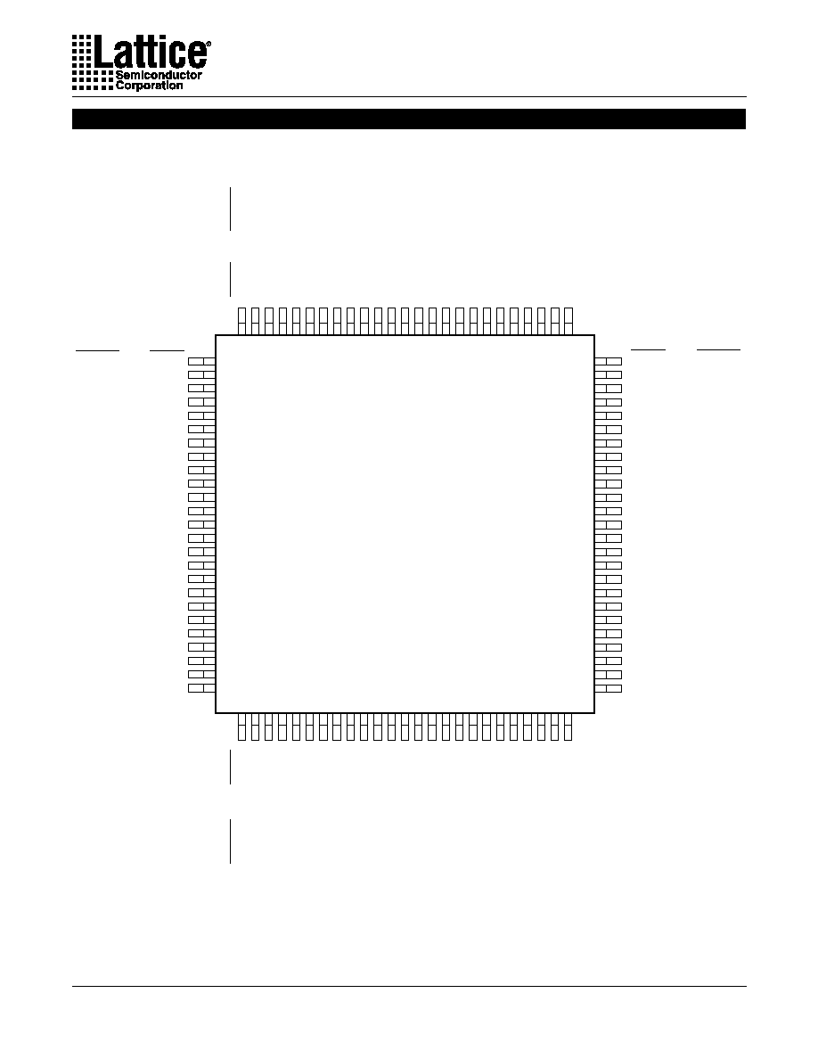
24
Specifications
ispGDX Family
Pin Configuration: ispGDX80A
ispGDX80A 100-Pin TQFP Pinout Diagram
I/O A0
I/O A1
I/O A2
I/O A3
I/O A4
GND
I/O A5
I/O A6
I/O A7
I/O A8
I/O A9
VCC
I/O A10
I/O A11
I/O A12
I/O A13
I/O A14
GND
I/O A15
I/O A16
I/O A17
I/O A18
I/O A19
I/O B0
I/O B1
I/O C19
I/O C18
I/O C17
I/O C16
I/O C15
GND
I/O C14
I/O C13
I/O C12
I/O C11
I/O C10
VCC
I/O C9
I/O C8
I/O C7
I/O C6
I/O C5
GND
I/O C4
I/O C3
I/O C2
I/O C1
I/O C0
1
2
3
4
5
6
7
8
9
10
11
12
13
14
15
16
17
18
19
20
21
22
23
24
25
75
74
73
72
71
70
69
68
67
66
65
64
63
62
61
60
59
57
56
55
54
53
52
51
26
27
28
29
30
31
32
33
34
35
36
37
38
39
40
41
42
43
44
45
46
47
48
49
50
100
99
98
97
96
95
94
93
92
91
90
89
88
87
86
85
84
83
82
81
80
79
78
77
76
58
ispGDX80A
Top View
Data
Control
CLK
OE
MUXsel1
MUXsel2
CLK
--
OE
MUXsel1
MUXsel2
CLK
OE
--
MUXsel1
MUXsel2
CLK
OE
MUXsel1
--
MUXsel2
CLK
OE
MUXsel1
MUXsel2
1. Pins have dual function capability.
CLK
OE
MUXsel2
MUXsel1
I/O D1
I/O D0
OE
CLK
OE
CLK
MUXsel2
--
MUXsel1
OE
CLK
MUXsel2
MUXsel1
--
OE
CLK
MUXsel2
MUXsel1
OE
--
CLK
MUXsel2
MUXsel1
OE
CLK
Data
Control
MUXsel2
MUXsel1
OE
CLK
MUXsel2
--
MUXsel1
OE
CLK
MUXsel2
MUXsel1
--
OE
CLK
MUXsel2
MUXsel1
OE
--
CLK
MUXsel2
MUXsel1
Data
Control
I/O D19
I/O D18
I/O D17
I/O D16
I/O D15
GND
I/O D14
I/O D13
I/O D12
I/O D11
I/O D10
VCC
--
RESET
--
TMS/MODE
1
--
Y1/TOE
1
I/O D9
I/O D8
I/O D7
I/O D6
I/O D5
GND
I/O D4
I/O D3
I/O D2
I/O B2
I/O B3
I/O B4
GND
I/O B5
I/O B6
I/O B7
I/O B8
I/O B9
I/O B10
1
TDI/SDI
I/O B11
I/O B12
I/O B13
I/O B14
GND
I/O B15
I/O B16
I/O B17
I/O B18
BSCAN/
ispEN
1
TCK/SCLK
VCC
Y0
Data
--
--
--
--
MUXsel1
MUXsel2
CLK
--
OE
MUXsel1
MUXsel2
CLK
OE
--
MUXsel1
MUXsel2
CLK
OE
MUXsel1
--
MUXsel2
CLK
OE
MUXsel1
MUXsel2
Control
I/O B19
TDO/SDO
1
--
25
Specifications
ispGDX Family
Part Number Description
Ordering Information
Table 2-0041/ispGDX
208-Pin PQFP
176-Pin TQFP
5
5
ispGDX160A-5Q208
272-Ball BGA
5
ispGDX160A-5B272
160A
208-Pin PQFP
7
ispGDX160A-7Q208
272-Ball BGA
7
ispGDX160A-7B272
208-Pin PQFP
5
ispGDX160-5Q208*
272-Ball BGA
5
ispGDX160-5B272*
160
208-Pin PQFP
7
ispGDX160-7Q208*
272-Ball BGA
7
ispGDX160-7B272*
ispGDX120A-5T176
120
80
160-Pin PQFP
5
ispGDX120A-5Q160
176-Pin TQFP
7
ispGDX120A-7T176
160-Pin PQFP
7
ispGDX120A-7Q160
100-Pin TQFP
5
ispGDX80A-5T100
100-Pin TQFP
7
ispGDX80A-7T100
I/O PINS
ORDERING NUMBER
PACKAGE
tpd (ns)
COMMERCIAL
*ispGDX160A recommended for new designs.
Device Number
160*
160A
120A
80A
Grade
Blank = Commercial
ispGDX XXXX
X XXXX X
Speed
5 = 5ns Tpd
7 = 7ns Tpd
Package
Q208 = PQFP (with Heat Spreader)
T176 = TQFP
Q160 = PQFP
B272 = BGA
T100 = TQFP
≠
Device Family
0212/ispGDX