Document Outline
- ispGDX80VA Data Sheet
- DC Electrical Characteristics
- AC Characteristics
- Pin Configuration: 100 TQFP
- Ordering Information

1
ispGDX
Æ
80VA
In-System Programmable
3.3V Generic Digital Crosspoint
Functional Block Diagram
Features
∑ IN-SYSTEM PROGRAMMABLE GENERIC DIGITAL
CROSSPOINT FAMILY
-- Advanced Architecture Addresses Programmable
PCB Interconnect, Bus Interface Integration and
Jumper/Switch Replacement
-- "Any Input to Any Output" Routing
-- Fixed HIGH or LOW Output Option for Jumper/DIP
Switch Emulation
-- Space-Saving PQFP and BGA Packaging
-- Dedicated IEEE 1149.1-Compliant Boundary Scan
Test
∑ HIGH PERFORMANCE E
2
CMOS
Æ
TECHNOLOGY
-- 3.3V Core Power Supply
-- 3.0ns Input-to-Output/3.0ns Clock-to-Output Delay
-- 250MHz Maximum Clock Frequency
-- TTL/3.3V/2.5V Compatible Input Thresholds and
Output Levels (Individually Programmable)
-- Low-Power: 16.5mA Quiescent Icc
-- 24mA I
OL
Drive with Programmable Slew Rate
Control Option
-- PCI Compatible Drive Capability
-- Schmitt Trigger Inputs for Noise Immunity
-- Electrically Erasable and Reprogrammable
-- Non-Volatile E
2
CMOS Technology
∑ ispGDXV OFFERS THE FOLLOWING ADVANTAGES
-- 3.3V In-System Programmable Using Boundary Scan
Test Access Port (TAP)
-- Change Interconnects in Seconds
∑ FLEXIBLE ARCHITECTURE
-- Combinatorial/Latched/Registered Inputs or Outputs
-- Individual I/O Tri-state Control with Polarity Control
-- Dedicated Clock/Clock Enable Input Pins (two) or
Programmable Clocks/Clock Enables from I/O Pins (20)
-- Single Level 4:1 Dynamic Path Selection (Tpd = 3.0ns)
-- Programmable Wide-MUX Cascade Feature
Supports up to 16:1 MUX
-- Programmable Pull-ups, Bus Hold Latch and Open
Drain on I/O Pins
-- Outputs Tri-state During Power-up ("Live Insertion"
Friendly)
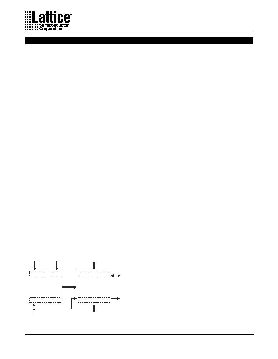
Global Routing
Pool
(GRP)
I/O
Cells
I/O Pins B
Boundary
Scan
Control
I/O
Cells
ISP
Control
I/O Pins
A
I/O Pins C
I/O Pins D
Description
The ispGDXVA architecture provides a family of fast,
flexible programmable devices to address a variety of
system-level digital signal routing and interface require-
ments including:
∑ Multi-Port Multiprocessor Interfaces
∑ Wide Data and Address Bus Multiplexing
(e.g. 16:1 High-Speed Bus MUX)
∑ Programmable Control Signal Routing
(e.g. Interrupts, DMAREQs, etc.)
∑ Board-Level PCB Signal Routing for Prototyping or
Programmable Bus Interfaces
The devices feature fast operation, with input-to-output
signal delays (Tpd) of 3.0ns and clock-to-output delays of
3.0ns.
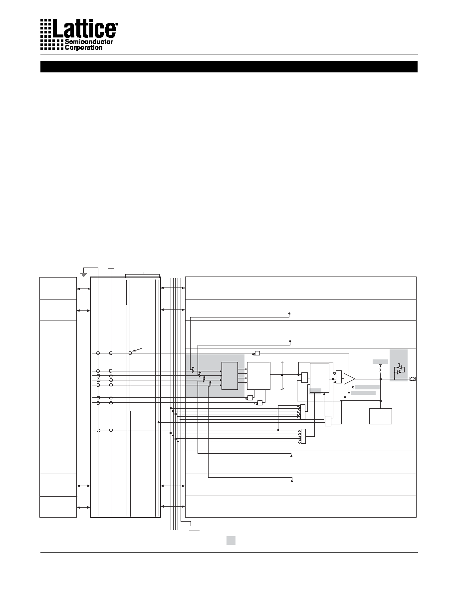
The architecture of the devices consists of a series of
programmable I/O cells interconnected by a Global Rout-
ing Pool (GRP). All I/O pin inputs enter the GRP directly
or are registered or latched so they can be routed to the
required I/O outputs. I/O pin inputs are defined as four
sets (A,B,C,D) which have access to the four MUX inputs
gdx80va_04
Copyright © 2002 Lattice Semiconductor Corporation. All brand or product names are trademarks or registered trademarks of their respective holders. The specifications and information herein
are subject to change without notice.
LATTICE SEMICONDUCTOR CORP., 5555 Northeast Moore Ct., Hillsboro, Oregon 97124, U.S.A.
February 2002
Tel. (503) 268-8000; 1-800-LATTICE; FAX (503) 268-8037; http://www.latticesemi.com
2
Specifications
ispGDX80VA
Description (Continued)
found in each I/O cell. Each output has individual, pro-
grammable I/O tri-state control (OE), output latch clock
(CLK), clock enable (CLKEN), and two multiplexer con-
trol (MUX0 and MUX1) inputs. Polarity for these signals
is programmable for each I/O cell. The MUX0 and MUX1
inputs control a fast 4:1 MUX, allowing dynamic selection
of up to four signal sources for a given output. A wider
16:1 MUX can be implemented with the MUX expander
feature of each I/O and a propagation delay increase of
2.0ns. OE, CLK, CLKEN, and MUX0 and MUX1 inputs
can be driven directly from selected sets of I/O pins.
Optional dedicated clock input pins give minimum clock-
to-output delays. CLK and CLKEN share the same set of
I/O pins. CLKEN disables the register clock when
CLKEN = 0.
Through in-system programming, connections between
I/O pins and architectural features (latched or registered
inputs or outputs, output enable control, etc.) can be
defined. In keeping with its data path application focus,
the ispGDXVA devices contain no programmable logic
arrays. All input pins include Schmitt trigger buffers for
noise immunity. These connections are programmed
into the device using non-volatile E
2
CMOS technology.
Non-volatile technology means the device configuration
is saved even when the power is removed from the
device.
In addition, there are no pin-to-pin routing constraints for
1:1 or 1:n signal routing. That is,
any I/O pin configured
as an input can drive one or more I/O pins configured as
outputs.
The device pins also have the ability to set outputs to
fixed HIGH or LOW logic levels (Jumper or DIP Switch
mode). Device outputs are specified for 24mA sink and
12mA source current (at JEDEC LVTTL levels) and can
be tied together in parallel for greater drive. On the
ispGDXVA, each I/O pin is individually programmable for
3.3V or 2.5V output levels as described later. Program-
mable output slew rate control can be defined
independently for each I/O pin to reduce overall ground
bounce and switching noise.
All I/O pins are equipped with IEEE1149.1-compliant
Boundary Scan Test circuitry for enhanced testability. In
addition, in-system programming is supported through
the Test Access Port via a special set of private com-
mands.
The ispGDXVA I/Os are designed to withstand "live
insertion" system environments. The I/O buffers are
disabled during power-up and power-down cycles. When
designing for "live insertion," absolute maximum rating
conditions for the Vcc and I/O pins must still be met.
Table 1. ispGDXVA Family Members
ispGDXV/VA Device
ispGDX160V/VA
I/O Pins
160
I/O-OE Inputs*
40
I/O-CLK / CLKEN Inputs*
40
I/O-MUXsel1 Inputs*
40
I/O-MUXsel2 Inputs*
40
BSCAN Interface
4
RESET
1
Pin Count/Package
208-Pin PQFP
208-Ball fpBGA
272-Ball BGA
* The CLK/CLK_EN, OE, MUX0 and MUX1 terminals on each I/O cell can each be assigned to
25% of the I/Os.
** Global clock pins Y0, Y1, Y2 and Y3 are multiplexed with CLKEN0, CLKEN1, CLKEN2 and
CLKEN3 respectively in all devices.
TOE
1
Dedicated Clock Pins**
4
EPEN
1
80
20
20
20
20
4
1
100-Pin TQFP
1
2
1
240
60
60
60
60
4
1
388-Ball fpBGA
1
4
1
ispGDX80VA
ispGDX240VA
3
Specifications
ispGDX80VA
Architecture
The ispGDXVA architecture is different from traditional
PLD architectures, in keeping with its unique application
focus. The block diagram is shown below. The program-
mable interconnect consists of a single Global Routing
Pool (GRP). Unlike ispLSI
Æ
devices, there are no pro-
grammable logic arrays on the device. Control signals for
OEs, Clocks/Clock Enables and MUX Controls must
come from designated sets of I/O pins. The polarity of
these signals can be independently programmed in each
I/O cell.
Each I/O cell drives a unique pin. The OE control for each
I/O pin is independent and may be driven via the GRP by
one of the designated I/O pins (I/O-OE set). The I/O-OE
set consists of 25% of the total I/O pins. Boundary Scan
test is supported by dedicated registers at each I/O pin.
In-system programming is accomplished through the
standard Boundary Scan protocol.
The various I/O pin sets are also shown in the block
diagram below. The A, B, C, and D I/O pins are grouped
together with one group per side.
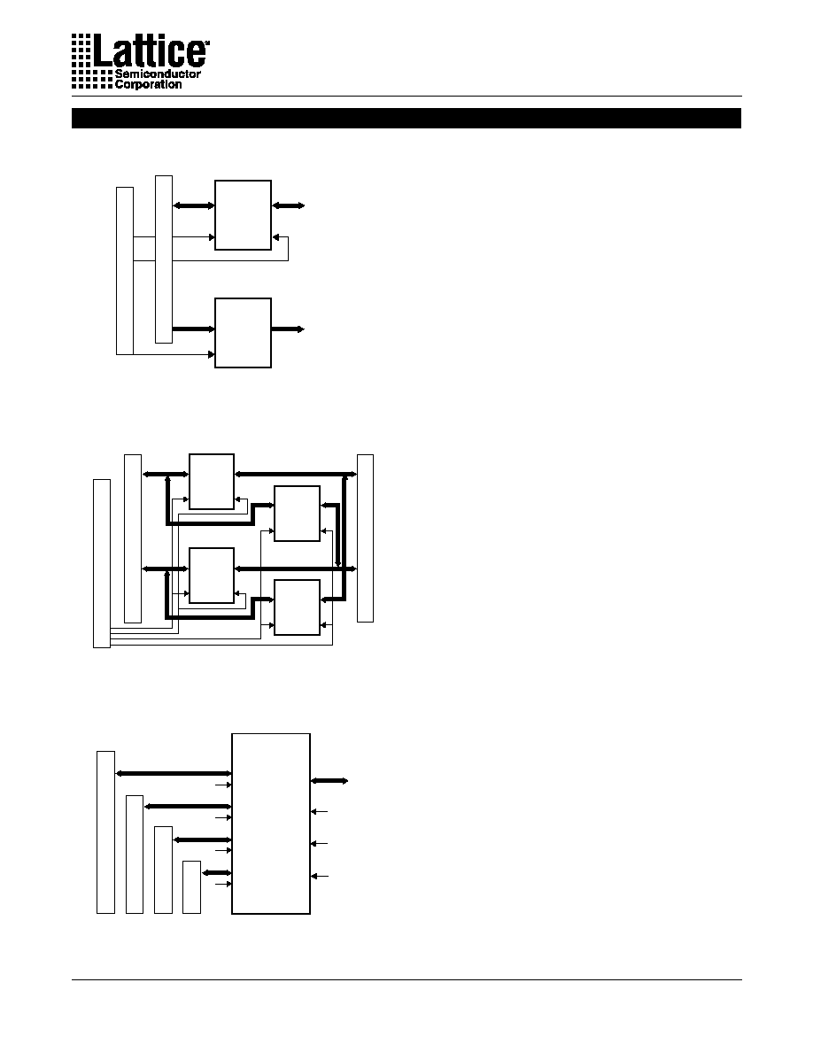
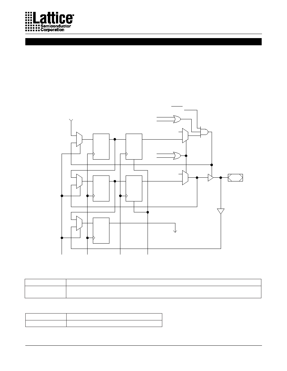
I/O Architecture
Each I/O cell contains a 4:1 dynamic MUX controlled by
two select lines as well as a 4x4 crossbar switch con-
trolled by software for increased routing flexiability (Figure
1). The four data inputs to the MUX (called M0, M1, M2,
and M3) come from I/O signals in the GRP and/or
adjacent I/O cells. Each MUX data input can access one
quarter of the total I/Os. For example, in an 80-I/O
ispGDXVA, each data input can connect to one of 20 I/O
pins. MUX0 and MUX1 can be driven by designated I/O
pins called MUXsel1 and MUXsel2. Each MUXsel input
covers 25% of the total I/O pins (e.g. 20 out of 80). MUX0
and MUX1 can be driven from either MUXsel1 or MUXsel2.
Figure 1. ispGDXVA I/O Cell and GRP Detail (80 I/O Device)
I/OCell 0
I/O Cell 1
I/O Cell 38
I/O Cell 39
40 I/O Cells
Boundary
Scan Cell
Bypass Option
I/O Cell N
Register
or Latch
I/O
Pin
Prog.
Pull-up
(VCCIO)
Prog. Slew Rate
D
A
B
CLK
Reset
Q
4-to-1 MUX
80 Input GRP
Inputs Vertical
Outputs Horizontal
I/O Cell 79
I/O Cell 78
I/O Cell 41
M0
I/O Group A
I/O Group B
I/O Group C
I/O Group D
M1
4x4
Crossbar
Switch
M2
M3
MUX1
MUX0
Global
Reset
I/O Cell 40
∑ ∑ ∑ ∑ ∑ ∑
∑
∑
∑
40 I/O Cells
ispGDXVA architecture enhancements over ispGDX (5V)
∑
∑
∑
∑
∑
∑
E
2
CMOS
Programmable
Interconnect
Logic "0" Logic "1"
80 I/O Inputs
C
R
Y0-Y3
Global
Clocks /
Clock_Enables
Prog.
Bus Hold
Latch
CLK_EN
From MUX Outputs
of 2 Adjacent I/O Cells
From MUX Outputs
of 2 Adjacent I/O Cells
To 2 Adjacent
I/O Cells above
To 2 Adjacent
I/O Cells below
Prog. Open Drain
2.5V/3.3V Output
∑
∑
∑
N+1
N+2
N-1
N-2
4
Specifications
ispGDX80VA
Flexible mapping of MUXsel
x
to MUX
x
allows the user to
change the MUX select assignment after the ispGDXVA
device has been soldered to the board. Figure 1 shows
that the I/O cell can accept (by programming the appro-
priate fuses) inputs from the MUX outputs of four adjacent
I/O cells, two above and two below. This enables cascad-
ing of the MUXes to enable wider (up to 16:1) MUX
implementations.
The I/O cell also includes a programmable flow-through
latch or register that can be placed in the input or output
path and bypassed for combinatorial outputs. As shown
in Figure 1, when the input control MUX of the register/
latch selects the "A" path, the register/latch gets its inputs
from the 4:1 MUX and drives the I/O output. When
selecting the "B" path, the register/latch is directly driven
by the I/O input while its output feeds the GRP. The
programmable polarity Clock to the latch or register can
be connected to any I/O in the I/O-CLK/CLKEN set (one-
quarter of total I/Os) or to one of the dedicated clock input
pins (Y
x
). The programmable polarity Clock Enable input
to the register can be programmed to connect to any of
the I/O-CLK/CLKEN input pin set or to the global clock
enable inputs (CLKEN
x
). Use of the dedicated clock
inputs gives minimum clock-to-output delays and mini-
mizes delay variation with fanout. Combinatorial output
mode may be implemented by a dedicated architecture
bit and bypass MUX. I/O cell output polarity can be
programmed as active high or active low.
MUX Expander Using Adjacent I/O Cells
The ispGDXVA allows adjacent I/O cell MUXes to be
cascaded to form wider input MUXes (up to 16 x 1)
without incurring an additional full Tpd penalty. However,
there are certain dependencies on the locality of the
adjacent MUXes when used along with direct MUX
inputs.
Adjacent I/O Cells
Expansion inputs MUXOUT[n-2], MUXOUT[n-1],
MUXOUT[n+1], and MUXOUT[n+2] are fuse-selectable
for each I/O cell MUX. These expansion inputs share the
same path as the standard A, B, C and D MUX inputs, and
allow adjacent I/O cell outputs to be directly connected
without passing through the global routing pool. The
relationship between the [N+i] adjacent cells and A, B, C
and D inputs will vary depending on where the I/O cell is
located on the physical die. The I/O cells can be grouped
into "normal" and "reflected" I/O cells or I/O "hemi-
spheres." These are defined as:
I/O MUX Operation
MUX1
MUX0
Data Input Selected
0
0
M0
0
1
M1
1
1
M2
1
0
M3
Device
Normal I/O Cells
Reflected I/O Cells
B9-B0, A19-A0,
D19-D10
B10-B19, C0-C19,
D0-D9
B19-B0, A39-A0,
D39-D20
B20-B39, C0-C39,
D0-D19
ispGDX80VA
ispGDX160VA
ispGDX240VA
B29-B0, A59-A0,
D59-D30
B30-B59, C0-C59,
D0-D29
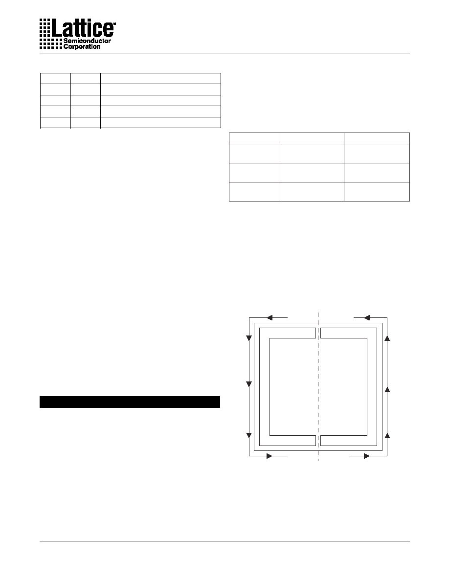
Table 2 shows the relationship between adjacent I/O
cells as well as their relationship to direct MUX inputs.
Note that the MUX expansion is circular and that I/O cell
B10, for example, draws on I/Os B9 and B8, as well as
B11 and B12, even though they are in different hemi-
spheres of the physical die. Table 2 shows some typical
cases and all boundary cases. All other cells can be
extrapolated from the pattern shown in the table.
D10
D9
B9
B10
A0
A19
C19
C0
D19
B0
D0
B19
I/O cell 0
I/O cell 79
I/O cell 39
I/O cell 40
I/O cell index increases in this direction
I/O cell index increases in this direction
Figure 2. I/O Hemisphere Configuration of
ispGDX80VA
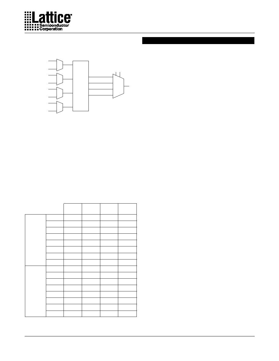
Direct and Expander Input Routing
Table 2 also illustrates the routing of MUX direct inputs
that are accessible when using adjacent I/O cells as
inputs. Take I/O cell D13 as an example, which is also
shown in Figure 3.
5
Specifications
ispGDX80VA
B10
B11
B12
B13
D6
D7
D8
D9
D10
D11
D12
D13
B6
B7
B8
B9
B12
B13
B14
B15
D8
D9
D10
D11
D8
D9
D10
D11
B4
B5
B6
B7
B11
B12
B13
B14
D7
D8
D9
D10
D9
D10
D11
D12
B5
B6
B7
B8
B9
B10
B11
B12
D5
D6
D7
D8
D11
D12
D13
D14
B7
B8
B9
B10
B8
B9
B10
B11
D4
D5
D6
D7
D12
D13
D14
D15
B8
B9
B10
B11
Data D/
MUXOUT
Data C/
MUXOUT
Data B/
MUXOUT
Data A/
MUXOUT
Reflected
I/O Cells
Normal
I/O Cells
Table 2. Adjacent I/O Cells (Mapping of
ispGDX80VA)
It can be seen from Figure 3 that if the D11 adjacent I/O
cell is used, the I/O group "A" input is no longer available
as a direct MUX input.
The ispGDXVA can implement MUXes up to 16 bits wide
in a single level of logic, but care must be taken when
combining adjacent I/O cell outputs with direct MUX
inputs. Any particular combination of adjacent I/O cells as
MUX inputs will dictate what I/O groups (A, B, C or D) can
be routed to the remaining inputs. By properly choosing
the adjacent I/O cells, all of the MUX inputs can be
utilized.
S0
S1
4 x 4
Crossbar
Switch
.m0
.m1
.m2
.m3
D13
I/O Group A
D11 MUX Out
I/O Group B
D12 MUX Out
I/O Group C
D14 MUX Out
I/O Group D
D15 MUX Out
ispGDX80VA I/O Cell
Figure 3. Adjacent I/O Cells vs. Direct Input Path for
ispGDX80VA, I/O D13
Special Features
Slew Rate Control
All output buffers contain a programmable slew rate
control that provides software-selectable slew rate op-
tions.
Open Drain Control
All output buffers provide a programmable Open-Drain
option which allows the user to drive system level reset,
interrupt and enable/disable lines directly without the
need for an off-chip Open-Drain or Open-Collector buffer.
Wire-OR logic functions can be performed at the printed
circuit board level.
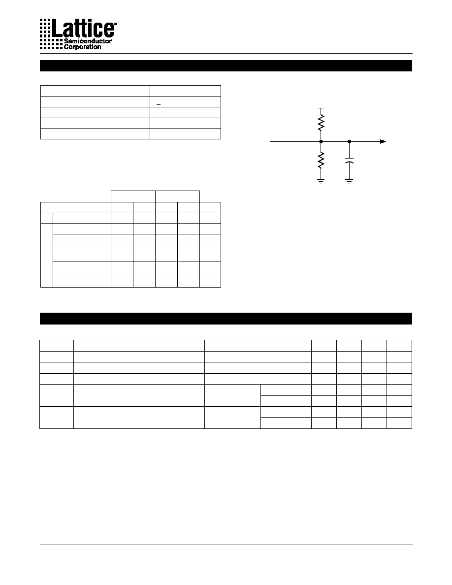
Pull-up Resistor
All pins have a programmable active pull-up. A typical
resistor value for the pull-up ranges from 50k
to 80k
.
Output Latch (Bus Hold)
All pins have a programmable circuit that weakly holds
the previously driven state when all drivers connected to
the pin (including the pin's output driver as well as any
other devices connected to the pin by external bus) are
tristated.
User-Programmable I/Os
The ispGDX80VA features user-programmable
I/Os supporting either 3.3V or 2.5V output voltage level
options. The ispGDX80VA uses a VCCIO pin to provide
the 2.5V reference voltage when used.
PCI Compatible Drive Capability
The ispGDX80VA supports PCI compatible drive capa-
bility for all I/Os.
6
Specifications
ispGDX80VA
The ispGDXVA Family architecture has been developed
to deliver an in-system programmable signal routing
solution with high speed and high flexibility. The devices
are targeted for three similar but distinct classes of end-
system applications:
Programmable, Random Signal
Interconnect (PRSI)
This class includes PCB-level programmable signal rout-
ing and may be used to provide arbitrary signal swapping
between chips. It opens up the possibilities of program-
mable system hardware. It is characterized by the need
to provide a large number of 1:1 pin connections which
are statically configured, i.e., the pin-to-pin paths do not
need to change dynamically in response to control in-
puts.
Programmable Data Path (PDP)
This application area includes system data path trans-
ceiver, MUX and latch functions. With today's 32- and
64-bit microprocessor buses, but standard data path glue
components still relegated primarily to eight bits, PCBs
are frequently crammed with a dozen or more data path
glue chips that use valuable real estate. Many of these
applications consist of "on-board" bus and memory inter-
faces that do not require the very high drive of standard
glue functions but can benefit from higher integration.
Therefore, there is a need for a flexible means to inte-
grate these on-board data path functions in an analogous
way to programmable logic's solution to control logic
integration. Lattice's CPLDs make an ideal control logic
complement to the ispGDXVA in-system programmable
data path devices as shown below.
Data Path
Bus #1
Control
Inputs
(from
µ
P)
Address
Inputs
(from
µ
P)
Control
Outputs
System
Clock(s)
Data Path
Bus #2
Configuration
(Switch)
Outputs
ISP/JTAG
Interface
ispLSI/
ispMACH
Device
ispGDXVA
Device
Buffers / Registers
Decoders
Buffers / Registers
State Machines
Figure 4. ispGDXVA Complements Lattice CPLDs
Applications
Programmable Switch Replacement (PSR)
Includes solid-state replacement and integration of me-
chanical DIP Switch and jumper functions. Through
in-system programming, pins of the ispGDXVA devices
can be driven to HIGH or LOW logic levels to emulate the
traditional device outputs. PSR functions do not require
any input pin connections.
These applications actually require somewhat different
silicon features. PRSI functions require that the device
support arbitrary signal routing on-chip between any two
pins with no routing restrictions. The routing connections
are static (determined at programming time) and each
input-to-output path operates independently. As a result,
there is little need for dynamic signal controls (OE,
clocks, etc.). Because the ispGDXVA device will inter-
face with control logic outputs from other components
(such as ispLSI or ispMACHTM) on the board (which
frequently change late in the design process as control
logic is finalized), there must be no restrictions on pin-to-
pin signal routing for this type of application.
PDP functions, on the other hand, require the ability to
dynamically switch signal routing (MUXing) as well as
latch and tri-state output signals. As a result, the pro-
grammable interconnect is used to define
possible signal
routes that are then selected dynamically by control
signals from an external MPU or control logic. These
functions are usually formulated early in the conceptual
design of a product. The data path requirements are
driven by the microprocessor, bus and memory architec-
ture defined for the system. This part of the design is the
earliest portion of the system design frozen, and will not
usually change late in the design because the result
would be total system and PCB redesign. As a result, the
ability to accommodate
arbitrary any pin-to-any pin re-
routing is not a strong requirement as long as the designer
has the ability to define his functions with a reasonable
degree of freedom initially.
As a result, the ispGDXVA architecture has been defined
to support PSR and PRSI applications (including bidirec-
tional paths) with no restrictions, while PDP applications
(using dynamic MUXing) are supported with a minimal
number of restrictions as described below. In this way,
speed and cost can be optimized and the devices can still
support the system designer's needs.
The following diagrams illustrate several ispGDXVA ap-
plications.
7
Specifications
ispGDX80VA
Figure 6. Data Bus Byte Swapper
Figure 7. Four-Port Memory Interface
Contr
ol Bus
Data Bus A
Data Bus B
OEA OEB
I/OA
D0-7
D8-15
D8-15
D0-7
I/OB
XCVR
OEA OEB
I/OA
I/OB
XCVR
OEA OEB
I/OA
I/OB
XCVR
OEA OEB
I/OA
I/OB
XCVR
Bus 4
Bus 3
Bus 2
Bus 1
Port #1
OE1
Memory
Port
OEM
SEL0
SEL1
To
Memory
Port #2
OE2
Port #3
OE3
Note: All OE and SEL lines driven by external arbiter logic (not shown).
Port #4
OE4
4-to-1
16-Bit MUX
Bidirectional
Figure 5. Address Demultiplex/Data Buffering
Contr
ol Bus
MUXed Ad
dress Data Bus
D
Q
CLK
OEA
OEB
I/OA
I/OB
Address
Buffered
Data
To Memory/
Peripherals
XCVR
Address
Latch
Applications (Continued)
Designing with the ispGDXVA
As mentioned earlier, this architecture satisfies the PRSI
class of applications without restrictions: any I/O pin as a
single input or bidirectional can drive any other I/O pin as
output.
For the case of PDP applications, the designer does have
to take into consideration the limitations on pins that can
be used as control (MUX0, MUX1, OE, CLK) or data
(MUXA-D) inputs. The restrictions on control inputs are
not likely to cause any major design issues because the
input possibilities span 25% of the total pins.
The MUXA-D input partitioning requires that designers
consciously assign pinouts so that MUX inputs are in the
appropriate, disjoint groups. For example, since the
MUXA group includes I/O A0-A19 (80 I/O device), it is not
possible to use I/O A0 and I/O A9 in the same MUX
function. As previously discussed, data path functions
will be assigned early in the design process and these
restrictions are reasonable in order to optimize speed
and cost.
User Electronic Signature
The ispGDXVA Family includes dedicated User Elec-
tronic Signature (UES) E
2
CMOS storage to allow users
to code design-specific information into the devices to
identify particular manufacturing dates, code revisions,
or the like. The UES information is accessible through
the boundary scan programming port via a specific com-
mand. This information can be read even when the
security cell is programmed.
Security
The ispGDXVA Family includes a security feature that
prevents reading the device program once set. Even
when set, it does not inhibit reading the UES or device ID
code. It can be erased only via a device bulk erase.
8
Specifications
ispGDX80VA
Absolute Maximum Ratings
1,2
Supply Voltage V
cc
................................. -0.5 to +5.4V
Input Voltage Applied ............................... -0.5 to +5.6V
Off-State Output Voltage Applied ............ -0.5 to +5.6V
Storage Temperature ................................ -65 to 150
∞
C
Case Temp. with Power Applied .............. -55 to 125
∞
C
Max. Junction Temp. (T
J
) with Power Applied ... 150
∞
C
1. Stresses above those listed under the "Absolute Maximum Ratings" may cause permanent damage to the device. Functional
operation of the device at these or at any other conditions above those indicated in the operational sections of this specification
is not implied (while programming, follow the programming specifications).
2. Compliance with the Thermal Management section of the Lattice Semiconductor Data Book or CD-ROM is a requirement.
DC Recommended Operating Conditions
C
SYMBOL
Table 2-0006/gdxva
C
PARAMETER
PACKAGE TYPE
Dedicated Clock Capacitance
8
UNITS
TYPICAL
TEST CONDITIONS
1
2
7
TQFP
TQFP
I/O Capacitance
pf
pf
V = 3.3V, V = 2.0V
V = 3.3V, V = 2.0V
CC
CC
Y
I/O
Capacitance (T
A
=25
o
C, f=1.0 MHz)
PARAMETER
MINIMUM
MAXIMUM
UNITS
Erase/Reprogram Cycles
10,000
--
Cycles
Erase/Reprogram Specifications
SYMBOL
Table 2-0005/gdxva
V
CC
V
CCIO
PARAMETER
Supply Voltage
I/O Reference Voltage
Commercial
T
A
= 0
∞
C to +70
∞
C
MIN.
MAX.
UNITS
3.00
2.3
3.60
3.60
V
Industrial
T
A
= -40
∞
C to +85
∞
C
3.00
3.60
V
V
9
Specifications
ispGDX80VA
Switching Test Conditions
Input Pulse Levels
Input Rise and Fall Time
Input Timing Reference Levels
Output Timing Reference Levels
Output Load
GND to V
CCIO(MIN)
<
1.5ns 10% to 90%
V
CCIO(MIN)
/2
V
CCIO(MIN)
/2
See Figure 8
3-state levels are measured 0.5V from steady-state active level.
Output Load Conditions (See Figure 8)
TEST CONDITION
R1
3.3V
2.5V
R2
CL
A
35pF
D
35pF
B
35pF
35pF
Active High
Slow Slew
Active Low
C
5pF
5pF
156
156
156
144
144
144
R1
R2
153
153
153
134
134
134
Active Low to Z
at V +0.5V
OL
Active High to Z
at V -0.5V
OH
Table 2-0004A/gdxva
DC Electrical Characteristics for 3.3V Range
Over Recommended Operating Conditions
Figure 8. Test Load
V
CCIO
R1
R2
CL
*
Device
Output
Test
Point
*
CL includes Test Fixture and Probe Capacitance.
0213D
V
OL
SYMBOL
1. Typical values are at V
CC
= 3.3V and T
A
= 25
∞
C.
Table 2-0007/gdxva
V
OH
V
IH
V
IL
PARAMETER
Output Low Voltage
Output High Voltage
Input High Voltage
Input Low Voltage
V
CC
=
V
CC (MIN)
I
OL
=
+100
µ
A
I
OL
=
+24mA
I
OH
=
-100
µ
A
I
OH
=
-12mA
V
CC
=
V
CC (MIN)
V
OH
V
OUT
or V
OUT
V
OL(MAX)
V
OH
V
OUT
or V
OUT
V
OL (MAX)
CONDITION
MIN.
TYP.
MAX.
UNITS
1
≠
2.8
2.0
-0.3
≠
≠
≠
≠
0.2
≠
5.25
0.8
V
≠
≠
0.55
V
V
2.4
≠
≠
V
V
CCIO
I/O Reference Voltage
3.0
≠
≠
3.6
V
V
V

10
Specifications
ispGDX80VA
DC Electrical Characteristics for 2.5V Range
Over Recommended Operating Conditions
V
IH
SYMBOL
2.5V/gdxva
V
OH
PARAMETER
Input High Voltage
Output High Voltage
V
OH(MIN)
V
OUT
or V
OUT
V
OL(MAX)
V
OH(MIN)
V
OUT
or V
OUT
V
OL(MAX)
V
CCIO=MIN
,
I
OH
=
-8mA
V
CCIO=MIN
,
I
OL
=
8mA
CONDITION
MIN.
TYP.
MAX.
UNITS
1.7
1.8
≠
≠
5.25
≠
V
V
CCIO
V
IL
I/O Reference Voltage
Input Low Voltage
2.3
-0.3
≠
≠
≠
2.7
0.7
V
V
V
V
CCIO=MIN
,
I
OH
=
-100µA
2.1
≠
≠
V
≠
≠
0.6
V
V
CCIO=MIN
,
I
OL
=
100µA
≠
≠
0.2
V
V
OL
Output Low Voltage
DC Electrical Characteristics
Over Recommended Operating Conditions
SYMBOL
1. One output at a time for a maximum of one second. V
OUT
=
0.5V was selected to avoid test problems by
tester ground degradation. Characterized, but not 100% tested.
2. Typical values are at V
CC
=
3.3V and T
A
=
25
∞
C.
3. I
CC
/ MHz = (0.002 x I/O cell fanout) + 0.022.
e.g. An input driving four I/O cells at 40MHz results in a dynamic I
CC
of approximately ((0.002 x 4) + 0.022) x 40 = 1.20mA.
4. For a typical application with 50% of I/O pins used as inputs, 50% used as outputs or bi-directionals.
5. This parameter limits the total current sinking of I/O pins surrounding the nearest GND pin.
DC Char_gdx80va
I
PU
I
BHLS
PARAMETER
I/O Active Pullup Current
Bus Hold Low Sustaining Current
I
IH
I
IL
Input or I/O High Leakage Current
Input or I/O Low Leakage Current
0V
V
IN
V
IL (MAX)
CONDITION
MIN.
TYP.
2
MAX.
UNITS
≠
≠
≠
≠
≠
≠
≠
≠
-10
10
-200
50
µ
A
I
BHT
Bus Hold Trip Points
V
IL
≠
V
IH
V
µ
A
µ
A
µ
A
40
≠
≠
µ
A
(V
CCIO
-0.2)
V
IN
V
CCIO
V
CCIO
V
IN
5.25V
0V
V
IN
V
IL (MAX)
I
OS
1
Output Short Circuit Current
≠
≠
-250
mA
V
CC
=
3.3V, V
OUT
=
0.5V, T
A
=
25
∞
C
I
CCQ
4
Quiescent Power Supply Current
≠
12
≠
mA
V
IL
=
0.5V, V
IH
=
V
CC
V
IN
=
V
IL (MAX)
I
BHHS
Bus Hold High Sustaining Current
-40
≠
≠
µ
A
V
IN
=
V
IH (MIN)
I
BHLO
Bus Hold Low Overdrive Current
≠
≠
550
µ
A
0V
V
IN
V
CCIO
I
CC
Dynamic Power Supply Current
per Input Switching
One input toggling at 50% duty cycle,
outputs open.
≠
See
Note 3
≠
mA/
MHz
I
CONT
5
Maximum Continuous I/O Pin Sink
Current Through Any GND Pin
≠
≠
≠
160
mA
I
BHHO
Bus Hold High Overdrive Current
≠
≠
-550
µ
A
0V
V
IN
V
CCIO
11
Specifications
ispGDX80VA
5.0
5.0
≠
≠
≠
≠
≠
≠
≠
≠
≠
≠
≠
≠
≠
≠
≠
≠
5.0
8.5
6.0
9.5
6.0
6.0
6.0
6.0
≠
≠
14.0
≠
5.0
0.5
1
2
3
4
5
6
7
8
9
10
11
12
13
14
15
16
17
18
19
20
21
22
23
24
25
26
27
28
29
30
31
32
Data Prop. Delay: Any I/O Pin to Any I/O Pin (4:1 MUX)
Data Prop. Delay: MUXsel Inputs to Any Output (4:1 MUX)
Clk. Frequency, Max. Toggle
Clk. Frequency with External Feedback
Input Latch or Reg. Setup Time Before Y
x
Input Latch or Reg. Setup Time Before I/O Clk.
Output Latch or Reg. Setup Time Before Y
x
Output Latch or Reg. Setup Time Before I/O Clk.
Global Clk. Enable Setup Time Before Y
x
Global Clk. Enable Setup Time Before I/O Clk.
I/O Clk. Enable Setup Time Before Y
x
Input Latch or Reg. Hold Time (Y
x
)
Input Latch or Reg. Hold Time (I/O Clk.)
Output Latch or Reg. Hold Time (Y
x
)
Output Latch or Reg. Hold Time (I/O Clk.)
Global Clk. Enable Hold Time (Y
x
)
Global Clk. Enable Hold Time (I/O Clk.)
I/O Clk. Enable Hold Time (Y
x
)
Output Latch or Reg. Clk. (from Y
x
) to Output Delay
Input Latch or Register Clk. (from Y
x
) to Output Delay
Output Latch or Reg. Clk. (from I/O pin) to Output Delay
Input Latch or Reg. Clk. (from I/O pin) to Output Delay
Input to Output Enable
Input to Output Disable
Test OE Output Enable
Test OE Output Disable
Clock Pulse Duration, High
Clock Pulse Duration, Low
Register Reset Delay from RESET Low
Reset Pulse Width
Output Delay Adder for Output Timings Using Slow Slew Rate
Output Skew (tgco1 Across Chip)
External Timing Parameters
Over Recommended Operating Conditions
ns
ns
MHz
MHz
ns
ns
ns
ns
ns
ns
ns
ns
ns
ns
ns
ns
ns
ns
ns
ns
ns
ns
ns
ns
ns
ns
ns
ns
ns
ns
ns
ns
≠
≠
143
111
4.0
3.0
4.0
3.0
2.5
1.5
4.5
0.0
1.5
0.0
1.5
0.0
1.5
0.0
≠
≠
≠
≠
≠
≠
≠
≠
3.5
3.5
≠
10.0
≠
≠
A
A
≠
≠
≠
≠
≠
≠
≠
≠
≠
≠
≠
≠
≠
≠
≠
≠
A
A
A
A
B
C
B
C
≠
≠
≠
≠
D
A
t
pd
2
t
sel
2
f
max (Tog.)
f
max (Ext.)
t
su1
t
su2
t
su3
t
su4
t
suce1
t
suce2
t
suce3
t
h1
t
h2
t
h3
t
h4
t
hce1
t
hce2
t
hce3
t
gco1
2
t
gco2
2
t
co1
2
t
co2
2
t
en
2
t
dis
2
t
toeen
2
t
toedis
2
t
wh
t
wl
t
rst
t
rw
t
sl
t
sk
DESCRIPTION
PARAMETER
( )
1
tsu3+tgco1
UNITS
-5
MIN. MAX.
1. All timings measured with one output switching, fast output slew rate setting, except
t
sl
.
2. The delay parameters are measured with Vcc as I/O voltage reference. An additional 0.5ns delay is incurred when Vccio is
used as I/O voltage reference.
3. The new "-3" speed grade (tpd = 3.0ns) will be effective starting with date code A113xxxx. Devices with topside date codes
prior to A113xxxx adhere to the shaded "-3" speed grade (tpd = 3.5ns).
#
3.0
3.2
≠
≠
≠
≠
≠
≠
≠
≠
≠
≠
≠
≠
≠
≠
≠
≠
3.0
5.5
3.5
6.0
4.0
4.0
5.5
5.5
≠
≠
7.0
≠
3.0
0.5
≠
≠
250
208.3
2.2
1.8
1.8
1.5
1.8
1.5
2.5
0.0
0.5
0.0
0.5
0.0
1.0
0.0
≠
≠
≠
≠
≠
≠
≠
≠
2.0
2.0
≠
4.5
≠
≠
-3
3
MIN. MAX.
TEST
1
COND.
3.5
3.5
≠
≠
≠
≠
≠
≠
≠
≠
≠
≠
≠
≠
≠
≠
≠
≠
3.5
6.0
4.0
7.0
5.0
5.0
6.0
6.0
≠
≠
8.0
≠
3.5
0.5
≠
≠
250
166.7
3.0
2.5
2.5
2.0
2.5
1.5
3.0
0.0
0.5
0.0
1.0
0.0
1.0
0.0
≠
≠
≠
≠
≠
≠
≠
≠
2.0
2.0
≠
5.0
≠
≠
-3
MIN. MAX.
12
Specifications
ispGDX80VA
9.0
9.0
≠
≠
≠
≠
≠
≠
≠
≠
≠
≠
≠
≠
≠
≠
≠
≠
9.0
13.5
11.5
15.7
10.5
10.5
10.5
10.5
≠
≠
22.0
≠
9.0
1.0
1
2
3
4
5
6
7
8
9
10
11
12
13
14
15
16
17
18
19
20
21
22
23
24
25
26
27
28
29
30
31
32
Data Prop. Delay: Any I/O pin to Any I/O Pin (4:1 MUX)
Data Prop. Delay: MUXsel Inputs to Any Output (4:1 MUX)
Clk. Frequency, Max. Toggle
Clk. Frequency with External Feedback
Input Latch or Reg. Setup Time Before Y
x
Input Latch or Reg. Setup Time Before I/O Clock
Output Latch or Reg. Setup Time Before Y
x
Output Latch or Reg. Setup Time Before I/O Clk.
Global Clk. Enable Setup Time Before Y
x
Global Clk. Enable Setup Time Before I/O Clk.
I/O Clk. Enable Setup Time Before Y
x
Input Latch or Reg. Hold Time (Y
x
)
Input Latch or Reg. Hold Time (I/O Clk.)
Output Latch or Reg. Hold Time (Y
x
)
Output Latch or Reg. Hold Time (I/O Clk.)
Global Clk. Enable Hold Time (Y
x
)
Global Clk. Enable Hold Time (I/O Clk.)
I/O Clk. Enable Hold Time (Y
x
)
Output Latch or Reg. Clk. (from Y
x
) to Output Delay
Input Latch or Reg. Clk. (from Y
x
) to Output Delay
Output Latch or Reg. Clk. (from I/O pin) to Output Delay
Input Latch or Reg. Clock (from I/O pin) to Output Delay
Input to Output Enable
Input to Output Disable
Test OE Output Enable
Test OE Output Disable
Clk. Pulse Duration, High
Clk. Pulse Duration, Low
Reg. Reset Delay from RESET Low
Reset Pulse Width
Output Delay Adder for Output Timings Using Slow Slew Rate
Output Skew (tgco1 Across Chip)
External Timing Parameters
Over Recommended Operating Conditions
ns
ns
MHz
MHz
ns
ns
ns
ns
ns
ns
ns
ns
ns
ns
ns
ns
ns
ns
ns
ns
ns
ns
ns
ns
ns
ns
ns
ns
ns
ns
ns
ns
≠
≠
83
62.5
7.0
6.0
7.0
6.0
4.0
3.0
8.5
0.0
3.0
0.0
3.0
0.0
3.0
0.0
≠
≠
≠
≠
≠
≠
≠
≠
6.0
6.0
≠
18.0
≠
≠
A
A
≠
≠
≠
≠
≠
≠
≠
≠
≠
≠
≠
≠
≠
≠
≠
≠
A
A
A
A
B
C
B
C
≠
≠
≠
≠
D
A
t
pd
2
t
sel
2
f
max (Tog.)
f
max (Ext.)
t
su1
t
su2
t
su3
t
su4
t
suce1
t
suce2
t
suce3
t
h1
t
h2
t
h3
t
h4
t
hce1
t
hce2
t
hce3
t
gco1
2
t
gco2
2
t
co1
2
t
co2
2
t
en
2
t
dis
2
t
toeen
2
t
toedis
2
t
wh
t
wl
t
rst
t
rw
t
sl
t
sk
DESCRIPTION
PARAMETER
( )
1
tsu3+tgco1
UNITS
-9
MIN. MAX.
1. All timings measured with one output switching, fast output slew rate setting, except
t
sl
.
2. The delay parameters are measured with Vcc as I/O voltage reference. An additional 0.5ns delay is incurred when Vccio is
used as I/O voltage reference.
#
-7
MIN. MAX.
TEST
1
COND.
≠
≠
100
80
5.5
4.5
5.5
4.5
3.5
2.5
6.5
0.0
2.5
0.0
2.5
0.0
2.5
0.0
≠
≠
≠
≠
≠
≠
≠
≠
5.0
5.0
≠
14.0
≠
≠
7.0
7.0
≠
≠
≠
≠
≠
≠
≠
≠
≠
≠
≠
≠
≠
≠
≠
≠
7.0
11.0
9.0
13.0
8.5
8.5
8.5
8.5
≠
≠
18.0
≠
7.0
0.5

13
Specifications
ispGDX80VA
External Timing Parameters (Continued)
1.0
0.0
0 4 10
20
30
40
50
60
70
0.2
0.4
0.6
0.8
1.2
1.4
1.6
GRP Delay (ns)
I/O Cell Fanout
ispGDX80VA Maximum
GRP Delay vs. I/O Cell Fanout
ispGDX80VA timings are specified with a GRP load
(fanout) of four I/O cells. The figure below shows the
GRP Delay with increased GRP loads. These deltas
apply to any signal path traversing the GRP (MUXA-D,
OE, CLK/CLKEN, MUXsel0-1). Global Clock signals
which do not use the GRP have no fanout delay adder.
14
Specifications
ispGDX80VA
-3
2
-3
-5
PARAMETER #
DESCRIPTION
1
MIN. MAX. MIN. MAX. MIN. MAX. UNITS
Inputs
t
io
32
Input Buffer Delay
--
0.3
--
0.4
--
0.9
ns
GRP
t
grp
33
GRP Delay
--
1.1
--
1.1
--
1.1
ns
MUX
t
muxd
34
I/O Cell MUX A/B/C/D Data Delay
--
0.8
--
1.0
--
1.5
ns
t
muxexp
35
I/O Cell MUX A/B/C/D Expander Delay
--
1.3
--
1.5
--
2.0
ns
t
muxs
36
I/O Cell Data Select
--
1.0
--
1.0
--
1.5
ns
t
muxsio
37
I/O Cell Data Select (I/O Clock)
--
1.5
--
1.5
--
3.0
ns
t
muxsg
38
I/O Cell Data Select (Yx Clock)
--
1.5
--
1.5
--
2.0
ns
t
muxselexp
39
I/O Cell MUX Data Select Expander Delay
--
1.5
--
1.5
--
2.0
ns
Register
t
iolat
40
I/O Latch Delay
--
1.0
--
1.0
--
1.0
ns
t
iosu
41
I/O Register Setup Time Before Clock
--
0.4
--
0.8
--
2.0
ns
t
ioh
42
I/O Register Hold Time After Clock
--
1.4
--
1.7
--
1.5
ns
t
ioco
43
I/O Register Clock to Output Delay
--
0.9
--
1.2
--
0.5
ns
t
ior
44
I/O Reset to Output Delay
--
1.0
--
1.0
--
1.5
ns
t
cesu
45
I/O Clock Enable Setup Time Before Clock
--
0.6
--
1.3
--
2.0
ns
t
ceh
46
I/O Clock Enable Hold Time After Clock
--
1.2
--
1.2
--
0.5
ns
Data Path
t
fdbk
47
I/O Register Feedback Delay
--
0.4
--
0.4
--
0.9
ns
t
iobp
48
I/O Register Bypass Delay
--
0.0
--
0.0
--
0.0
ns
t
ioob
49
I/O Register Output Buffer Delay
--
0.0
--
0.0
--
0.0
ns
t
muxcg
50
I/O Register A/B/C/D Data Input MUX Delay (Yx Clock)
--
1.3
--
1.5
--
2.0
ns
t
muxcio
51
I/O Register A/B/C/D Data Input MUX Delay (I/O Clock)
--
1.3
--
1.5
--
3.0
ns
t
iodg
52
I/O Register I/O MUX Delay (Yx Clock)
--
3.1
--
3.5
--
4.0
ns
t
iodio
53
I/O Register I/O MUX Delay (I/O Clock)
--
3.1
--
3.5
--
5.0
ns
Outputs
t
ob
54
Output Buffer Delay
--
0.8
--
1.0
--
1.5
ns
t
obs
55
Output Buffer Delay (Slow Slew Option)
--
3.8
--
4.5
--
6.5
ns
t
oeen
56
I/O Cell OE to Output Enable
--
2.6
--
3.5
--
4.0
ns
t
oedis
57
I/O Cell OE to Output Disable
--
2.6
--
3.5
--
4.0
ns
t
goe
58
GRP Output Enable and Disable Delay
--
0.0
--
0.0
--
0.0
ns
t
toe
59
Test OE Enable and Disable Delay
--
2.5
--
2.5
--
2.0
ns
Clocks
t
ioclk
60
I/O Clock Delay
--
0.3
--
0.3
--
2.0
ns
t
gclk
61
Global Clock Delay
--
1.3
--
1.3
--
2.0
ns
t
gclkeng
62
Global Clock Enable (Yx Clock)
--
2.5
--
2.5
--
2.5
ns
t
gclkenio
63
Global Clock Enable (I/O Clock)
--
2.0
--
2.0
--
3.5
ns
t
ioclkeng
64
I/O Clock Enable (Yx Clock)
--
1.5
--
1.5
--
2.5
ns
Global Reset
t
gr
65
Global Reset to I/O Register Latch
--
5.2
--
6.0
--
11.0
ns
Internal Timing Parameters
Over Recommended Operating Conditions
1. Internal Timing Parameters are not tested and are for reference only.
2. The new "-3" speed grade (tpd = 3.0ns) will be effective starting with date code A113xxxx. Devices with topside date codes prior to
A113xxxx adhere to the shaded "-3" speed grade (tpd = 3.5ns).
Timing Rev. 2.9
15
Specifications
ispGDX80VA
-7
-9
PARAMETER #
DESCRIPTION
1
MIN. MAX. MIN. MAX. UNITS
Inputs
t
io
32
Input Buffer Delay
--
1.4
--
1.9
ns
GRP
t
grp
33
GRP Delay
--
1.1
--
1.1
ns
MUX
t
muxd
34
I/O Cell MUX A/B/C/D Data Delay
--
2.0
--
2.5
ns
t
muxexp
35
I/O Cell MUX A/B/C/D Expander Delay
--
2.5
--
3.0
ns
t
muxs
36
I/O Cell Data Select
--
2.0
--
2.5
ns
t
muxsio
37
I/O Cell Data Select (I/O Clock)
--
4.5
--
6.0
ns
t
muxsg
38
I/O Cell Data Select (Yx Clock)
--
2.5
--
3.0
ns
t
muxselexp
39
I/O Cell MUX Data Select Expander Delay
--
2.5
--
3.0
ns
Register
t
iolat
40
I/O Latch Delay
--
1.0
--
1.0
ns
t
iosu
41
I/O Register Setup Time Before Clock
--
3.2
--
4.4
ns
t
ioh
42
I/O Register Hold Time After Clock
--
2.3
--
2.6
ns
t
ioco
43
I/O Register Clock to Output Delay
--
0.5
--
0.5
ns
t
ior
44
I/O Reset to Output Delay
--
1.5
--
1.5
ns
t
cesu
45
I/O Clock Enable Setup Time Before Clock
--
2.5
--
2.0
ns
t
ceh
46
I/O Clock Enable Hold Time After Clock
--
1.0
--
2.0
ns
Data Path
t
fdbk
47
I/O Register Feedback Delay
--
1.2
--
1.3
ns
t
iobp
48
I/O Register Bypass Delay
--
0.3
--
0.6
ns
t
ioob
49
I/O Register Output Buffer Delay
--
0.6
--
0.7
ns
t
muxcg
50
I/O Register A/B/C/D Data Input MUX Delay (Yx Clock)
--
2.5
--
3.0
ns
t
muxcio
51
I/O Register A/B/C/D Data Input MUX Delay (I/O Clock)
--
4.5
--
6.0
ns
t
iodg
52
I/O Register I/O MUX Delay (Yx Clock)
--
5.0
--
6.0
ns
t
iodio
53
I/O Register I/O MUX Delay (I/O Clock)
--
7.0
--
9.0
ns
Outputs
t
ob
54
Output Buffer Delay
--
2.2
--
2.9
ns
t
obs
55
Output Buffer Delay (Slow Slew Option)
--
9.2
--
11.9
ns
t
oeen
56
I/O Cell OE to Output Enable
--
6.0
--
7.5
ns
t
oedis
57
I/O Cell OE to Output Disable
--
6.0
--
7.5
ns
t
goe
58
GRP Output Enable and Disable Delay
--
0.0
--
0.0
ns
t
toe
59
Test OE Enable and Disable Delay
--
2.5
--
3.0
ns
Clocks
t
ioclk
60
I/O Clock Delay
--
3.2
--
4.4
ns
t
gclk
61
Global Clock Delay
--
2.7
--
3.4
ns
t
gclkeng
62
Global Clock Enable (Yx Clock)
--
3.7
--
5.4
ns
t
gclkenio
63
Global Clock Enable (I/O Clock)
--
5.7
--
8.4
ns
t
ioclkeng
64
I/O Clock Enable (Yx Clock)
--
4.2
--
6.4
ns
Global Reset
t
gr
65
Global Reset to I/O Register Latch
--
13.7
--
16.4
ns
Internal Timing Parameters
1
Over Recommended Operating Conditions
1. Internal Timing Parameters are not tested and are for reference only.
2. Refer to the Timing Model in this data sheet for further details.
Timing Rev. 2.9
16
Specifications
ispGDX80VA
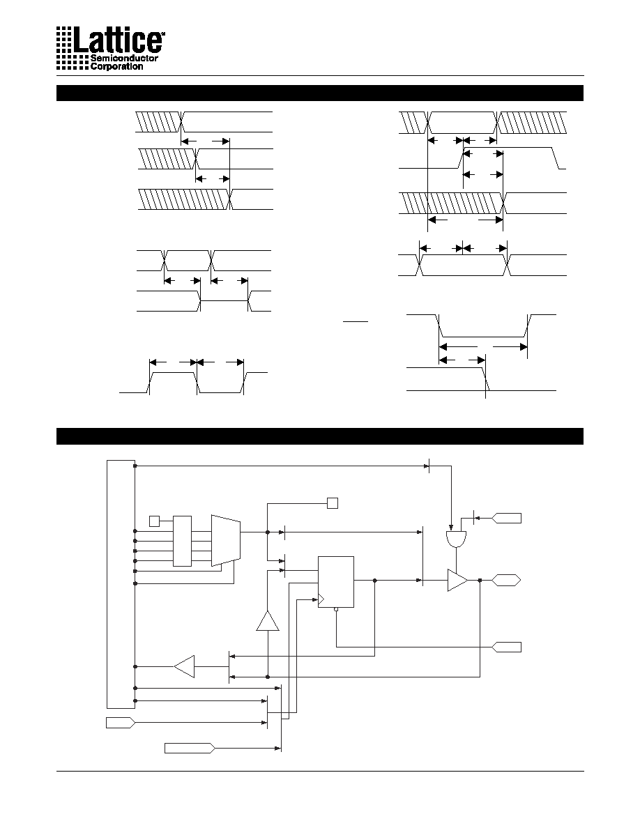
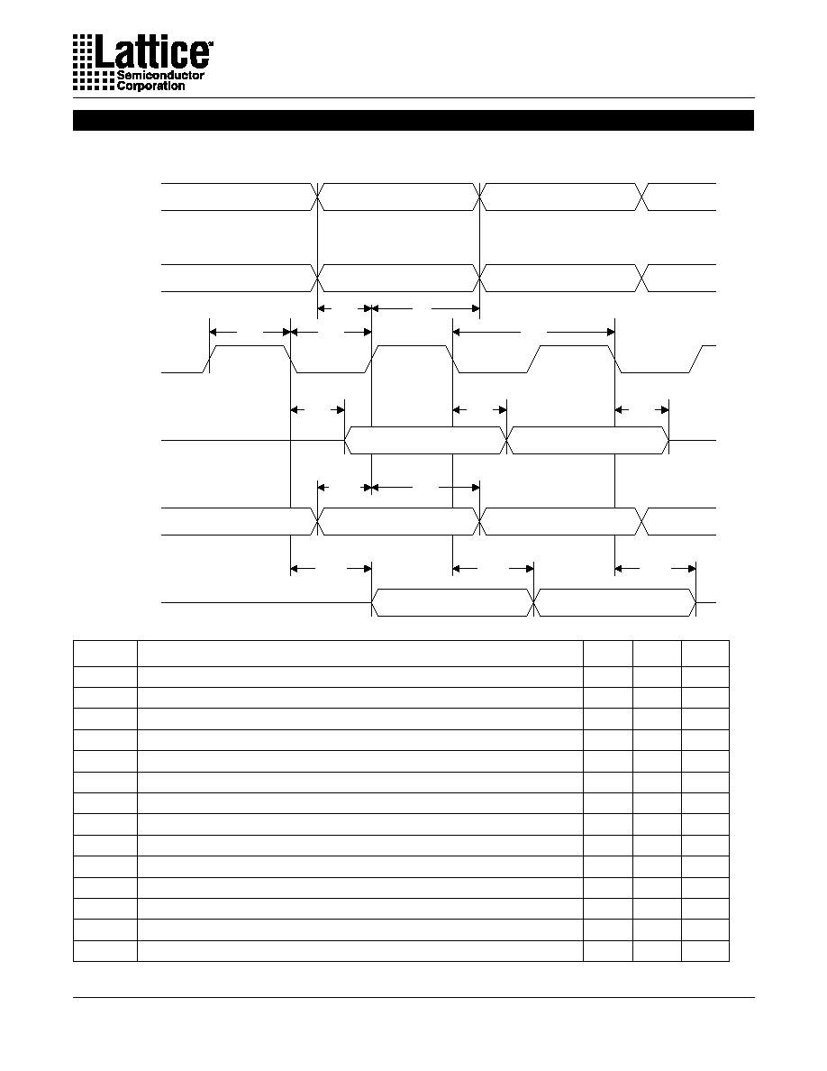
Switching Waveforms
Clock Width
CLK
(I/O INPUT)
t
wl
t
wh
COMBINATORIAL
I/O OUTPUT
VALID INPUT
DATA (I/O INPUT)
t
pd
t
sel
VALID INPUT
MUXSEL (I/O INPUT)
Combinatorial Output
COMBINATORIAL
I/O OUTPUT
OE (I/O INPUT)
t
en
t
dis
I/O Output Enable/Disable
Registered Output
Reset
REGISTERED
I/O OUTPUT
t
rst
RESET
t
rw
I/O Pin
RESET
TOE
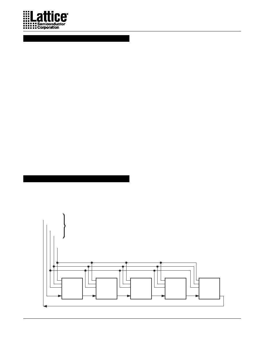
Y0,1,2,3
Y0,1,2,3, Enable
tgclk #61
tgclkeng #62
tgclkenio #63
MUX0
MUX1
tgrp #33
MUX Expander Input
GRP
A
B
C
D
OE
tgoe #58
tmuxexp #35
tmuxselexp #39
tiobp #48
CLK
CLKEN
MUX Expander Output
tioob #49
tmuxd #34
tmuxs #36
tmuxio #37
tmuxg #38
tmuxcg #50
tmuxcio #51
tiod #52, #53
tgr #65
0902/gdxv/va
tio #32
tfdbk #47
tioclk #60
tioclkeg #64
tiolat #40
tiosu #41
tioh #42
tioco #43
tior #44
tcesu #45
tceh #46
tob #54
tobs #55
toeen #56
toedis #57
ttoe #59
CLK
CLKEN
D
Q
DATA
(I/O INPUT)
REGISTERED
I/O OUTPUT
CLK
CLKEN
VALID INPUT
t
t
h
t
suce
t
ceh
t
co
1/
f
max
(external fdbk)
t
gco
su
ispGDXVA Timing Model
17
Specifications
ispGDX80VA
ispLEVER Development System
The ispLEVER Development System supports ispGDX
design using a VHDL or Verilog language syntax. From
creation to in-system programming, the ispLEVER sys-
tem is an easy-to-use, self-contained design tool.
Features
∑ VHDL and Verilog Synthesis Support Available
∑ ispGDX Design Compiler
- Design Rule Checker
- I/O Connectivity Checker
- Automatic Compiler Function
∑ Industry Standard JEDEC File for Programming
∑ Min/Max Timing Report
∑ Interfaces To Popular Timing Simulators
∑ User Electronic Signature (UES) Support
∑ Detailed Log and Report Files For Easy Design
Debug
∑ On-line Help
∑ Windows
Æ
XP, Windows 2000, Windows 98 and
Windows NT
Æ
Compatible
∑ Solaris
Æ
and HP-UX Versions Available
In-System Programmability
All necessary programming of the ispGDXVA is done via
four TTL level logic interface signals. These four signals
are fed into the on-chip programming circuitry where a
state machine controls the programming.
On-chip programming can be accomplished using an
IEEE 1149.1 boundary scan protocol. The IEEE 1149.1-
compliant interface signals are Test Data In (TDI), Test
Data Out (TDO), Test Clock (TCK) and Test Mode Select
(TMS) control. The EPEN pin is also used to enable or
disable the JTAG port.
The embedded controller port enable pin (EPEN) is used
to enable the JTAG tap controller and in that regard has
similar functionality to a TRST pin. When the pin is driven
high, the JTAG TAP controller is enabled. This is also true
when the pin is left unconnected, in which case the pin is
pulled high by the permanent internal pullup. This allows
ISP programming and BSCAN testing to take place as
specified by the Instruction Table.
When the pin is driven low, the JTAG TAP controller is
driven to a reset state asynchronously. It stays there
while the pin is held low. After pulling the pin high the
JTAG controller becomes active. The intent of this fea-
ture is to allow the JTAG interface to be directly controlled
by the data bus of an embedded controller (hence the
name Embedded Port Enable). The EPEN signal is used
as a "device select" to prevent spurious programming
and/or testing from occuring due to random bit patterns
on the data bus. Figure 9 illustrates the block diagram for
the ispJTAGTM interface.
Figure 9. ispJTAG Device Programming Interface
ispGDX
80VA
Device
TDO
TDI
TMS
TCK
EPEN
ispJTAG
Programming
Interface
ispLSI
Device
ispMACH
Device
ispGDX
80VA
Device
ispGDX
80VA
Device
18
Specifications
ispGDX80VA
Boundary Scan
The ispGDXVA devices provide IEEE1149.1a test capa-
bility and ISP programming through a standard Boundary
Scan Test Access Port (TAP) interface.
The boundary scan circuitry on the ispGDXVA Family
operates independently of the programmed pattern. This
allows customers using boundary scan test to have full
test capability with only a single BSDL file.
The ispGDXVA devices are identified by the 32-bit JTAG
IDCODE register. The device ID assignments are listed
in Table 4.
Table 3. I/O Shift Register Order
Figure 10. Boundary Scan Register Circuit for I/O Pins
Normal
Function
OE
EXTEST
Update DR
SCANOUT
(to next cell)
Clock DR
SCANIN
(from previous
cell
Shift DR
Normal
Function
TOE
D
Q
D
Q
D
Q
D
Q
D
Q
I/O Pin
Reset
BSCAN
Registers
BSCAN
Latches
HIGHZ
0
1
0
1
PROG_MODE
EXTEST
I/O Shift Reg Order/ispGDXVA
ispGDX80VA
TDI, TOE,
RESET
, Y1, Y0, I/O B10 .. B19, I/O C0 .. C19, I/O D0 .. D9, I/O B9 .. B0, I/O A19.. A0,
I/O D19 .. D10, TDO
I/O SHIFT REGISTER ORDER
DEVICE
Table 4. ispGDX80VA Device ID Codes
ID Code/GDX80VA
ispGDX80VA
0001, 0000, 0011, 0101, 0000, 0000, 0100, 0011
32-BIT BOUNDARY SCAN ID CODE
DEVICE
19
Specifications
ispGDX80VA
The ispJTAG programming is accomplished by execut-
ing Lattice private instructions under the Boundary Scan
State Machine.
Details of the programming sequence are transparent to
the user and are handled by Lattice ISP Daisy Chain
1
0
0
1
1
0
0
1
0
0
0
0
1
0
1
1
0
1
0
1
1
1
0
1
0
0
1
1
1
0
0
1
Update-IR
Exit2-IR
Pause-IR
Exit1-IR
Shift-IR
Capture-IR
Select-IR-Scan
Update-DR
Exit2-DR
Pause-DR
Exit1-DR
Shift-DR
Capture-DR
Select-DR-Scan
Run-Test/Idle
Test-Logic-Reset
Figure 12. Boundary Scan State Machine
Figure 11. Boundary Scan Register Circuit for Input-Only Pins
Downlowad software, ispCODE `C' routines or any third-
party programmers. Contact Lattice Technical Support to
obtain more detailed programming information.
SCANOUT
(to next cell)
Clock DR
SCANIN
(from previous
cell
Shift DR
D
Q
Input Pin
Boundary Scan (Continued)
20
Specifications
ispGDX80VA
Symbol
Parameter
Min
Max
Units
t
btcp
TCK [BSCAN test] clock pulse width
100
≠
ns
t
btch
TCK [BSCAN test] pulse width high
50
≠
ns
tbtcl
TCK [BSCAN test] pulse width low
50
≠
ns
tbtsu
TCK [BSCAN test] setup time
20
≠
ns
tbth
TCK [BSCAN test] hold time
25
≠
ns
trf
TCK [BSCAN test] rise and fall time
50
≠
mV/ns
tbtco
TAP controller falling edge of clock to valid output
≠
25
ns
tbtoz
TAP controller falling edge of clock to data output disable
≠
25
ns
tbtvo
TAP controller falling edge of clock to data output enable
≠
25
ns
tbtcpsu
BSCAN test Capture register setup time
20
≠
ns
tbtcph
BSCAN test Capture register hold time
25
≠
ns
tbtuco
BSCAN test Update reg, falling edge of clock to valid output
≠
50
ns
tbtuoz
BSCAN test Update reg, falling edge of clock to output disable
≠
50
ns
tbtuov
BSCAN test Update reg, falling edge of clock to output enable
≠
50
ns
Figure 13. Boundary Scan Waveforms and Timing Specifications
TMS
TDI
TCK
TDO
Data to be
captured
Data to be
driven out
Valid Data
Valid Data
Valid Data
Valid Data
Data Captured
btsu
T
bth
T
btcl
T
btch
T
btcp
T
btvo
T
btco
T
btoz
T
btcsu
T
btch
T
btuov
T
btuco
T
btuoz
T
Boundary Scan (Continued)
21
Specifications
ispGDX80VA
I/O
Input/Output Pins ≠ These are the general purpose bidirectional data pins. When used as outputs,
each may be independently latched, registered or tristated. They can also each assume one other
control function (OE, CLK/CLKEN, and MUXsel as described in the text).
RESET
/ I/O D10
This pin can be configured by the user through software to act as a
RESET
pin or as an I/O (I/O D10)
The default is
RESET
. If programmed to act as
RESET
, this pin is an active LOW Input Pin and resets
all I/O Register outputs when LOW.
Y1/CLKEN1/TOE,
Input Pins ≠ These can be either Global Clocks or Clock Enables. In addition, Y1 is multiplexed with
Y0/CLKEN0
TOE. Each pin can drive any or all I/O cell registers. The Test Output Enable (TOE) pin tristates all I/O
pins when LOW
EPEN
Input Pin ≠ JTAG TAP Controller Enable Pin. When high, JTAG operation is enabled. When low,
JTAG TAP controller is driven to reset.
TDI
Input Pin ≠ Serial data input during ISP programming or Boundary Scan mode.
TCK
Input Pin ≠ Serial data clock during ISP programming or Boundary Scan mode.
TMS
Input Pin ≠ Control input during ISP programming or Boundary Scan mode.
TDO
Output Pin ≠ Serial data output during ISP programming or Boundary Scan mode.
GND
Ground (GND)
VCC
Vcc ≠ Supply voltage (3.3V).
VCCIO
Input ≠ This pin is used if optional 2.5V output is to be used. Every I/O can independently select either
3.3V or the optional voltage as its output level. If the optional output voltage is not required, this pin
must be connected to the VCC supply. Programmable pull-up resistors and bus-hold latches only draw
current from this supply.
Signal Descriptions
Signal Name Description
22
Specifications
ispGDX80VA
I/O
Control
100
Signal
Signal
TQFP
Signal Locations: ispGDX80VA
Signal
100-Pin TQFP
RESET
/I/O D10
90
Y0/CLKEN0
38
Y1/CLKEN1/TOE 87
EPEN
35
TDI
39
TCK
36
TMS
86
TDO
85
GND
6, 18, 29, 45, 56, 68, 79, 95
VCC
12, 37, 62, 88
VCCIO
89
I/O A0
CLK
1
I/O A1
OE
2
I/O A2
MUXsel1
3
I/O A3
MUXsel2
4
I/O A4
CLK
5
GND
I/O A5
OE
7
I/O A6
MUXsel1
8
I/O A7
MUXsel2
9
I/O A8
CLK
10
I/O A9
OE
11
VCC
I/O A10
MUXsel1
13
I/O A11
MUXsel2
14
I/O A12
CLK
15
I/O A13
OE
16
I/O A14
MUXsel1
17
GND
I/O A15
MUXsel2
19
I/O A16
CLK
20
I/O A17
OE
21
I/O A18
MUXsel1
22
I/O A19
MUXsel2
23
I/O B0
CLK
24
I/O B1
OE
25
I/O B2
MUXsel1
26
I/O B3
MUXsel2
27
I/O B4
CLK
28
GND
I/O B5
OE
30
I/O B6
MUXsel1
31
I/O B7
MUXsel2
32
I/O B8
CLK
33
I/O B9
OE
34
VCC
I/O B10
MUXsel1
40
I/O B11
MUXsel2
41
I/O B12
CLK
42
I/O B13
OE
43
I/O B14
MUXsel1
44
GND
I/O B15
MUXsel2
46
I/O B16
CLK
47
I/O B17
OE
48
I/O B18
MUXsel1
49
I/O B19
MUXsel2
50
I/O C0
CLK
51
I/O C1
OE
52
I/O Locations: ispGDX80VA
I/O
Control
100
Signal
Signal
TQFP
I/O
Control
100
Signal
Signal
TQFP
I/O
Control
100
Signal
Signal
TQFP
*I/O D10 is multiplexed with
RESET
. The functionality is programmable and selected through software.
Note: VCC and GND Pads Shown for Reference
I/O C2
MUXsel1
53
I/O C3
MUXsel2
54
I/O C4
CLK
55
GND
I/O C5
OE
57
I/O C6
MUXsel1
58
I/O C7
MUXsel2
59
I/O C8
CLK
60
I/O C9
OE
61
VCC
I/O C10
MUXsel1
63
I/O C11
MUXsel2
64
I/O C12
CLK
65
I/O C13
OE
66
I/O C14
MUXsel1
67
GND
I/O C15
MUXsel2
69
I/O C16
CLK
70
I/O C17
OE
71
I/O C18
MUXsel1
72
I/O C19
MUXsel2
73
I/O D0
CLK
74
I/O D1
OE
75
I/O D2
MUXsel1
76
I/O D3
MUXsel2
77
I/O D4
CLK
78
GND
I/O D5
OE
80
I/O D6
MUXsel1
81
I/O D7
MUXsel2
82
I/O D8
CLK
83
I/O D9
OE
84
VCC
VCCIO
I/O D10*
MUXsel1
90
I/O D11
MUXsel2
91
I/O D12
CLK
92
I/O D13
OE
93
I/O D14
MUXsel1
94
GND
I/O D15
MUXsel2
96
I/O D16
CLK
97
I/O D17
OE
98
I/O D18
MUXsel1
99
I/O D19
MUXsel2
100
23
Specifications
ispGDX80VA
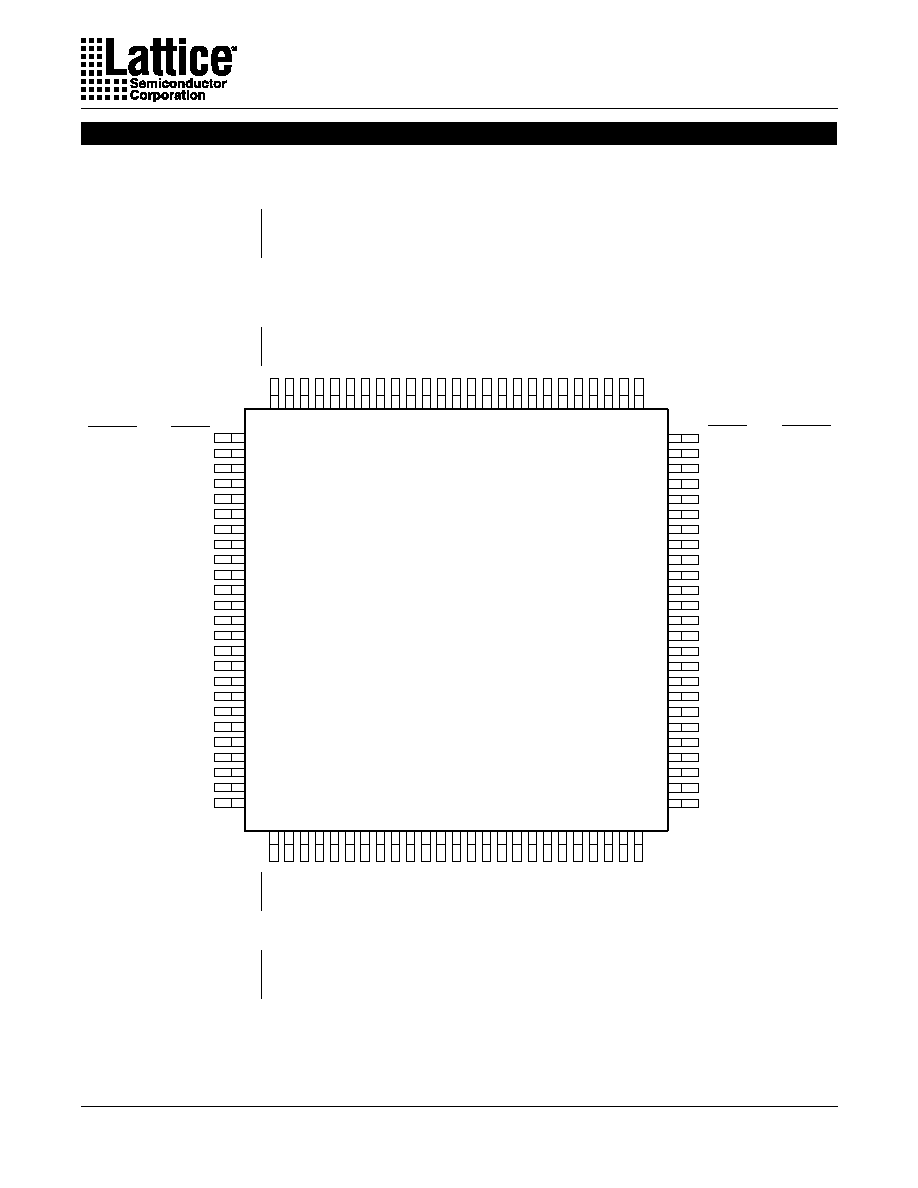
Pin Configuration: ispGDX80VA
ispGDX80VA 100-Pin TQFP Pinout Diagram
I/O A0
I/O A1
I/O A2
I/O A3
I/O A4
GND
I/O A5
I/O A6
I/O A7
I/O A8
I/O A9
VCC
I/O A10
I/O A11
I/O A12
I/O A13
I/O A14
GND
I/O A15
I/O A16
I/O A17
I/O A18
I/O A19
I/O B0
I/O B1
I/O C19
I/O C18
I/O C17
I/O C16
I/O C15
GND
I/O C14
I/O C13
I/O C12
I/O C11
I/O C10
VCC
I/O C9
I/O C8
I/O C7
I/O C6
I/O C5
GND
I/O C4
I/O C3
I/O C2
I/O C1
I/O C0
1
2
3
4
5
6
7
8
9
10
11
12
13
14
15
16
17
18
19
20
21
22
23
24
25
75
74
73
72
71
70
69
68
67
66
65
64
63
62
61
60
59
57
56
55
54
53
52
51
26
27
28
29
30
31
32
33
34
35
36
37
38
39
40
41
42
43
44
45
46
47
48
49
50
100
99
98
97
96
95
94
93
92
91
90
89
88
87
86
85
84
83
82
81
80
79
78
77
76
58
ispGDX80VA
Top View
Data
Control
CLK
OE
MUXsel1
MUXsel2
CLK
OE
MUXsel1
MUXsel2
CLK
OE
MUXsel1
MUXsel2
CLK
OE
MUXsel1
MUXsel2
CLK
OE
MUXsel1
MUXsel2
CLK
OE
MUXsel2
MUXsel1
I/O D1
I/O D0
OE
CLK
OE
CLK
MUXsel2
MUXsel1
OE
CLK
MUXsel2
MUXsel1
OE
CLK
MUXsel2
MUXsel1
OE
CLK
MUXsel2
MUXsel1
OE
CLK
Data
Control
MUXsel2
MUXsel1
OE
CLK
MUXsel2
MUXsel1
OE
CLK
MUXsel2
MUXsel1
OE
CLK
MUXsel2
MUXsel1
OE
CLK
MUXsel2
MUXsel1
Data
Control
I/O D19
I/O D18
I/O D17
I/O D16
I/O D15
GND
I/O D14
I/O D13
I/O D12
I/O D11
RESET
/I/O D10
VCC
VCCIO
TMS
Y1/CLKEN1/TOE
I/O D9
I/O D8
I/O D7
I/O D6
I/O D5
GND
I/O D4
I/O D3
I/O D2
I/O B2
I/O B3
I/O B4
GND
I/O B5
I/O B6
I/O B7
I/O B8
I/O B9
I/O B10
TDI
I/O B11
I/O B12
I/O B13
I/O B14
GND
I/O B15
I/O B16
I/O B17
I/O B18
EPEN
TCK
VCC
Y0/CLKEN0
Data
MUXsel1
MUXsel2
CLK
OE
MUXsel1
MUXsel2
CLK
OE
MUXsel1
MUXsel2
CLK
OE
MUXsel1
MUXsel2
CLK
OE
MUXsel1
MUXsel2
Control
I/O B19
TDO
24
Specifications
ispGDX80VA
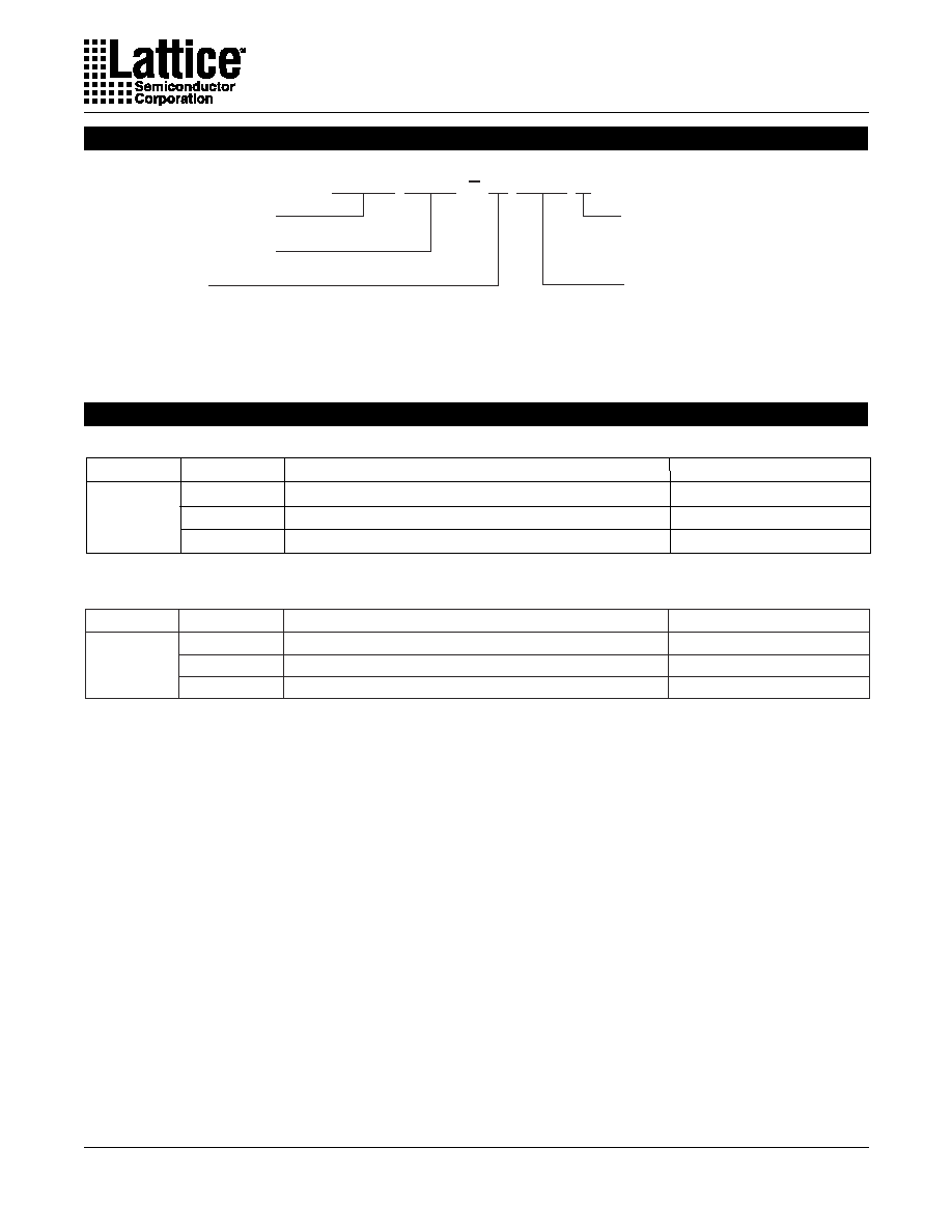
Part Number Description
Ordering Information
Device Number
Grade
Blank = Commercial
I = Industrial
ispGDX 80VA
X XXXX X
Speed
3 = 3.0ns Tpd*
5 = 5.0ns Tpd
7 = 7.0ns Tpd
9 = 9.0ns Tpd
Package
T100 = 100-Pin TQFP
Device Family
0212/gdx80va
Table 2-0041A/gdx80va
100-Pin TQFP
5.0
ispGDX80VA-5T100
ispGDXVA
100-Pin TQFP
3.0*
ispGDX80VA-3T100
100-Pin TQFP
7.0
ispGDX80VA-7T100
FAMILY
ORDERING NUMBER
PACKAGE
tpd (ns)
COMMERCIAL
Table 2-0041/gdx80va
100-Pin TQFP
9.0
ispGDX80VA-9T100I
100-Pin TQFP
7.0
ispGDX80VA-7T100I
100-Pin TQFP
5.0
ispGDX80VA-5T100I
ispGDXVA
FAMILY
ORDERING NUMBER
PACKAGE
tpd (ns)
INDUSTRIAL
Note: The ispGDX80VA devices are dual-marked with both Commercial and Industrial grades. The Commercial speed
grade is faster, e.g. ispGDX80VA-3T100-5I.
*The new "-3" speed grade (tpd = 3.0ns) will be effective starting with date code A113xxxx.