1
ispLSI
Æ
1032
In-System Programmable High Density PLD
USE ispLSI 1032E FOR NEW
COMMERCIAL & INDUSTRIAL
DESIGNS
Features
∑ HIGH-DENSITY PROGRAMMABLE LOGIC
-- High Speed Global Interconnect
-- 6000 PLD Gates
-- 64 I/O Pins, Eight Dedicated Inputs
-- 192 Registers
-- Wide Input Gating for Fast Counters, State
Machines, Address Decoders, etc.
-- Small Logic Block Size for Fast Random Logic
-- Security Cell Prevents Unauthorized Copying
∑ HIGH PERFORMANCE E
2
CMOS
Æ
TECHNOLOGY
--
f
max = 90 MHz Maximum Operating Frequency
--
f
max = 60 MHz for Industrial and Military/883 Devices
--
t
pd = 12 ns Propagation Delay
-- TTL Compatible Inputs and Outputs
-- Electrically Erasable and Reprogrammable
-- Non-Volatile E
2
CMOS Technology
-- 100% Tested
∑ IN-SYSTEM PROGRAMMABLE
-- In-System ProgrammableTM (ISPTM) 5-Volt Only
-- Increased Manufacturing Yields, Reduced Time-to-
Market, and Improved Product Quality
-- Reprogram Soldered Devices for Faster Prototyping
∑ COMBINES EASE OF USE AND THE FAST SYSTEM
SPEED OF PLDs WITH THE DENSITY AND FLEX-
IBILITY OF FIELD PROGRAMMABLE GATE ARRAYS
-- Complete Programmable Device Can Combine Glue
Logic and Structured Designs
-- Four Dedicated Clock Input Pins
-- Synchronous and Asynchronous Clocks
-- Flexible Pin Placement
-- Optimized Global Routing Pool Provides Global
Interconnectivity
∑ ispDesignEXPERTTM ≠ LOGIC COMPILER AND COM-
PLETE ISP DEVICE DESIGN SYSTEMS FROM HDL
SYNTHESIS THROUGH IN-SYSTEM PROGRAMMING
-- Superior Quality of Results
-- Tightly Integrated with Leading CAE Vendor Tools
-- Productivity Enhancing Timing Analyzer, Explore
Tools, Timing Simulator and ispANALYZERTM
-- PC and UNIX Platforms
1032_07
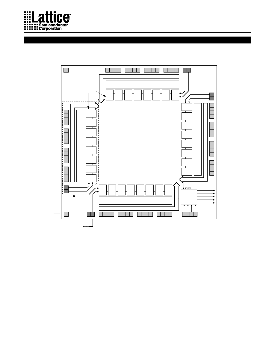
Functional Block Diagram
Output Routing Pool
Output Routing Pool
D7 D6 D5 D4 D3 D2 D1 D0
B0 B1 B2 B3 B4 B5 B6 B7
A0
A1
A2
A3
A4
A5
A6
A7
C7
C6
C5
C4
C3
C2
C1
C0
Output Routing Pool
CLK
Output Routing Pool
Global Routing Pool (GRP)
Logic
Array
D Q
D Q
D Q
D Q
GLB
Description
The ispLSI 1032 is a High-Density Programmable Logic
Device containing 192 Registers, 64 Universal I/O pins,
eight Dedicated Input pins, four Dedicated Clock Input
pins and a Global Routing Pool (GRP). The GRP pro-
vides complete interconnectivity between all of these
elements. The ispLSI 1032 features 5-Volt in-system
programming and in-system diagnostic capabilities. It is
the first device which offers non-volatile reprogrammability
of the logic, as well as the interconnect to provide truly
reconfigurable systems.
The basic unit of logic on the ispLSI 1032 device is the
Generic Logic Block (GLB). The GLBs are labeled A0, A1
.. D7 (see figure 1). There are a total of 32 GLBs in the
ispLSI 1032 device. Each GLB has 18 inputs, a program-
mable AND/OR/XOR array, and four outputs which can
be configured to be either combinatorial or registered.
Inputs to the GLB come from the GRP and dedicated
inputs. All of the GLB outputs are brought back into the
GRP so that they can be connected to the inputs of any
other GLB on the device.
Copyright © 1999 Lattice Semiconductor Corp. All brand or product names are trademarks or registered trademarks of their respective holders. The specifications and information herein are subject
to change without notice.
LATTICE SEMICONDUCTOR CORP., 5555 Northeast Moore Ct., Hillsboro, Oregon 97124, U.S.A.
March 1999
Tel. (503) 268-8000; 1-800-LATTICE; FAX (503) 268-8556; http://www.latticesemi.com
Specifications
ispLSI 1032
2
Functional Block Diagram
Figure 1. ispLSI 1032 Functional Block Diagram
The device also has 64 I/O cells, each of which is directly
connected to an I/O pin. Each I/O cell can be individually
programmed to be a combinatorial input, registered in-
put, latched input, output or bi-directional I/O pin with
3-state control. Additionally, all outputs are polarity se-
lectable, active high or active low. The signal levels are
TTL compatible voltages and the output drivers can
source 4 mA or sink 8 mA.
Eight GLBs, 16 I/O cells, two dedicated inputs and one
ORP are connected together to make a Megablock (see
figure 1). The outputs of the eight GLBs are connected to
a set of 16 universal I/O cells by the ORP. The I/O cells
within the Megablock also share a common Output
Enable (OE) signal. The ispLSI 1032 device contains four
of these Megablocks.
The GRP has as its inputs the outputs from all of the GLBs
and all of the inputs from the bi-directional I/O cells. All of
these signals are made available to the inputs of the
GLBs. Delays through the GRP have been equalized to
minimize timing skew.
Clocks in the ispLSI 1032 device are selected using the
Clock Distribution Network. Four dedicated clock pins
(Y0, Y1, Y2 and Y3) are brought into the distribution
network, and five clock outputs (CLK 0, CLK 1, CLK 2,
IOCLK 0 and IOCLK 1) are provided to route clocks to the
GLBs and I/O cells. The Clock Distribution Network can
also be driven from a special clock GLB (C0 on the ispLSI
1032 device). The logic of this GLB allows the user to
create an internal clock from a combination of internal
signals within the device.
Y
0
Y
1
Y
2
Y
3
I/O 0
I/O 1
I/O 2
I/O 3
IN 5
IN 4
I/O 6
I/O 7
I/O 8
I/O 9
I/O 10
I/O 11
I/O 12
I/O 13
I/O 14
I/O 15
I/O 47
I/O 46
I/O 45
I/O 44
I/O 43
I/O 42
I/O 41
I/O 40
I/O 39
I/O 38
I/O 37
I/O 36
I/O 35
I/O 34
I/O 33
I/O 32
SDI/IN 0
MODE/IN 1
I/O
62
I/O
63
I/O
61
I/O
60
I/O
59
I/O
58
I/O
57
I/O
56
I/O
55
I/O
54
I/O
53
I/O
52
I/O
51
I/O
50
I/O
49
I/O
48
IN
7
IN
6
I/O
17
I/O
16
I/O
18
I/O
19
I/O
20
I/O
21
I/O
22
I/O
23
I/O
24
I/O
25
I/O
26
I/O
27
I/O
28
I/O
29
I/O
30
I/O
31
SDO/IN 2
SCLK/IN 3
I/O 4
I/O 5
RESET
Global
Routing
Pool
(GRP)
Output Routing Pool (ORP)
Output Routing Pool (ORP)
CLK 0
CLK 1
CLK 2
IOCLK 0
IOCLK 1
Clock
Distribution
Network
D7
D6
D5
D4
D3
D2
D1
D0
B0
B1
B2
B3
B4
B5
B6
B7
A0
A1
A2
A3
A4
A5
A6
A7
C7
C6
C5
C4
C3
C2
C1
C0
Output Routing Pool (ORP)
Generic
Logic Blocks
(GLBs)
Megablock
Output Routing Pool (ORP)
Input Bus
Input Bus
Input Bus
ispEN
lnput Bus
0139(1)-32-isp
Specifications
ispLSI 1032
3
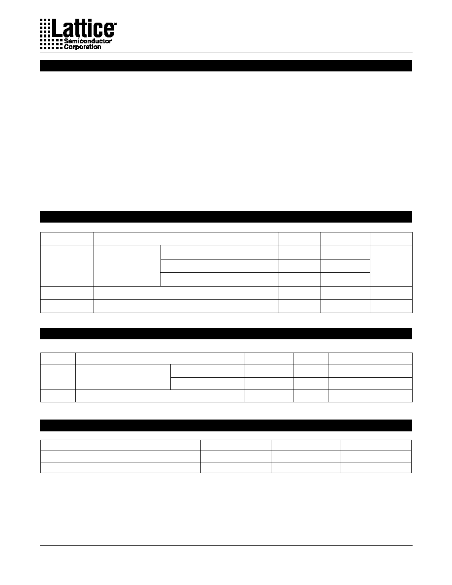
Absolute Maximum Ratings
1
Supply Voltage V
cc
.................................. -0.5 to +7.0V
Input Voltage Applied ........................ -2.5 to V
CC
+1.0V
Off-State Output Voltage Applied ..... -2.5 to V
CC
+1.0V
Storage Temperature ................................ -65 to 150
∞
C
Case Temp. with Power Applied .............. -55 to 125
∞
C
Max. Junction Temp. (T
J
) with Power Applied ... 150
∞
C
1. Stresses above those listed under the "Absolute Maximum Ratings" may cause permanent damage to the device. Functional
operation of the device at these or at any other conditions above those indicated in the operational sections of this specification
is not implied (while programming, follow the programming specifications).
DC Recommended Operating Conditions
V
V
PARAMETER
SYMBOL
MIN.
MAX.
UNITS
5.25
5.5
5.5
0.8
Vcc + 1
Supply Voltage
V
CC
V
IL
V
IH
Table 2- 0005Aisp w/mil.eps
4.75
4.5
4.5
0
2.0
Commercial T
A
=
0
∞
C to +70
∞
C
Industrial
T
A
= -40
∞
C to +85
∞
C
Military/883
T
C
= -55
∞
C to +125
∞
C
Input Low Voltage
Input High Voltage
V
Capacitance (T
A
=25
o
C, f=1.0 MHz)
SYMBOL
PARAMETER
MAXIMUM
1
UNITS
TEST CONDITIONS
C
1
Commercial/Industrial
8
pf
V
CC
=5.0V, V
IN
=2.0V
Military
10
pf
V
CC
=5.0V, V
IN
=2.0V
C
2
I/O and Clock Capacitance
10
pf
V
CC
=5.0V, V
I/O
, V
Y
=2.0V
1
.
Guaranteed but not 100% tested.
Table 2- 0006
Dedicated Input Capacitance
Data Retention Specifications
Table 2- 0008B
PARAMETER
Data Retention
MINIMUM
MAXIMUM
UNITS
Erase/Reprogram Cycles
20
10000
--
--
Years
Cycles
Specifications
ispLSI 1032
4
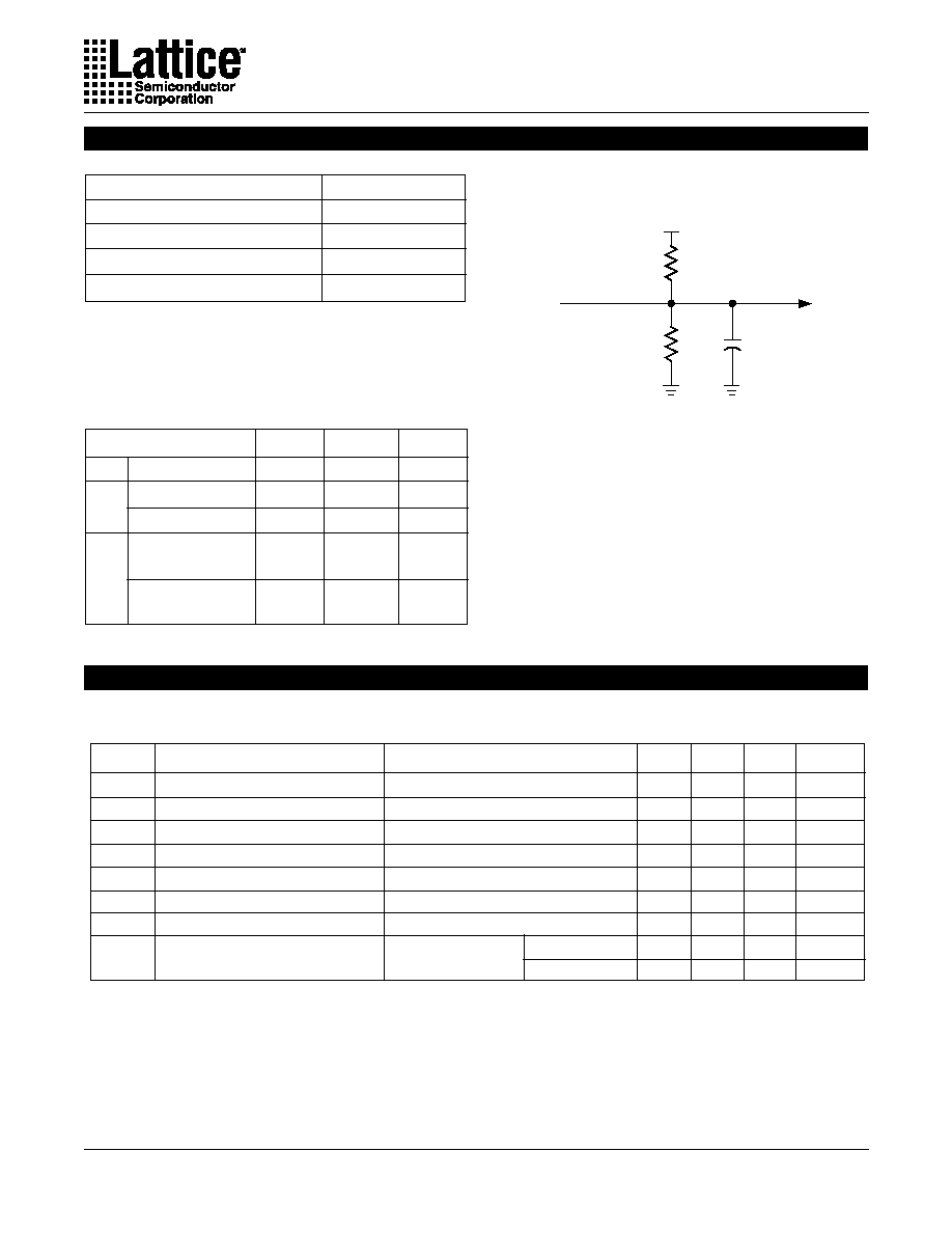
Switching Test Conditions
Input Pulse Levels
GND to 3.0V
Input Rise and Fall Time
3ns 10% to 90%
Input Timing Reference Levels
1.5V
Output Timing Reference Levels
1.5V
Output Load
See figure 2
3-state levels are measured 0.5V from steady-state
active level.
Table 2- 0003
Output Load Conditions (see figure 2)
Test Condition
R1
R2
CL
A
470
390
35pF
B
Active High
390
35pF
Active Low
470
390
35pF
Active High to Z
390
5pF
C
at V
OH
- 0.5V
Active Low to Z
470
390
5pF
at V
OL
+ 0.5V
Figure 2. Test Load
+ 5V
R1
R2
CL
*
Device
Output
Test
Point
*
CL includes Test Fixture and Probe Capacitance.
DC Electrical Characteristics
Over Recommended Operating Conditions
0.4
≠
-10
10
-150
-150
-200
190
220
V
V
µ
A
µ
A
µ
A
µ
A
mA
mA
mA
SYMBOL
V
OL
V
OH
I
IL
I
IH
I
IL-isp
I
IL-PU
I
OS
1
I
CC
2,4
Output Low Voltage
Output High Voltage
Input or I/O Low Leakage Current
Input or I/O High Leakage Current
isp Input Low Leakage Current
I/O Active Pull-Up Current
Output Short Circuit Current
Operating Power Supply Current
I
OL
=8 mA
I
OH
=-4 mA
0V
V
IN
V
IL
(MAX.)
3.5V
V
IN
V
CC
0V
V
IN
V
IL
(MAX.)
0V
V
IN
V
IL
V
CC
= 5V, V
OUT
= 0.5V
V
IL
= 0.5V, V
IH
= 3.0V Commercial
f
TOGGLE
= 1 MHz
Industrial/Military
PARAMETER
CONDITION
MIN.
UNITS
MAX.
TYP.
3
≠
≠
≠
≠
≠
≠
≠
130
135
≠
2.4
≠
≠
≠
≠
≠
≠
≠
1. One output at a time for a maximum duration of one second.
2. Measured using eight 16-bit counters.
3. Typical values are at V
CC
= 5V and T
A
= 25
o
C.
4. Maximum I
CC
varies widely with specific device configuration and operating frequency. Refer to the Power Consumption sec-
tion of this datasheet and Thermal Management section of the Lattice Semiconductor Data Book or CD-ROM to estimate maximum
I
CC
.
Table 2- 0007A-32-isp
Specifications
ispLSI 1032
5
USE 1032E-100
FOR NEW DESIGNS
USE 1032E-70
FOR NEW DESIGNS
USE 1032E-70
FOR NEW DESIGNS
1. Unless noted otherwise, all parameters use a GRP load of 4 GLBs, 20 PTXOR path, ORP and Y0 clock.
2. Refer to Timing Model in this data sheet for further details.
3. Standard 16-Bit counter using GRP feedback.
4. fmax (Toggle) may be less than 1/(twh + twl). This is to allow for a clock duty cycle of other than 50%.
5. Reference Switching Test Conditions section.
MIN. MAX.
Data Propagation Delay, 4PT bypass, ORP bypass
Data Propagation Delay, Worst Case Path
Clock Frequency with Internal Feedback
3
Clock Frequency with External Feedback
Clock Frequency, Max Toggle
4
GLB Reg. Setup Time before Clock, 4PT bypass
GLB Reg. Clock to Output Delay, ORP bypass
GLB Reg. Hold Time after Clock, 4 PT bypass
GLB Reg. Setup Time before Clock
GLB Reg. Clock to Output Delay
GLB Reg. Hold Time after Clock
Ext. Reset Pin to Output Delay
Ext. Reset Pulse Duration
Input to Output Enable
Input to Output Disable
Ext. Sync. Clock Pulse Duration, High
Ext. Sync. Clock Pulse Duration, Low
I/O Reg. Setup Time before Ext. Sync. Clock (Y2, Y3)
I/O Reg. Hold Time after Ext. Sync. Clock (Y2, Y3)
ns
ns
MHz
MHz
MHz
ns
ns
ns
ns
ns
ns
ns
ns
ns
ns
ns
ns
ns
ns
t
pd1
t
pd2
f
max (Int.)
f
max (Ext.)
f
max (Tog.)
t
su1
t
co1
t
h1
t
su2
t
co2
t
h2
t
r1
t
rw1
t
en
t
dis
t
wh
t
wl
t
su5
t
h5
1
2
3
4
5
6
7
8
9
10
11
12
13
14
15
16
17
18
19
A
A
A
≠
≠
≠
A
≠
≠
≠
≠
A
≠
B
C
≠
≠
≠
≠
DESCRIPTION
1
PARAMETER
#
2
UNITS
TEST
5
COND.
1
tsu2 + tco1
( )
MIN. MAX.
≠
≠
80
50
100
7
≠
0
10
≠
0
≠
10
≠
≠
5
5
2
6.5
15
20
≠
≠
≠
≠
10
≠
≠
12
≠
17
≠
18
18
≠
≠
≠
≠
≠
≠
60
38
83
9
≠
0
13
≠
0
≠
13
≠
≠
6
6
2.5
8.5
20
25
≠
≠
≠
≠
13
≠
≠
16
≠
22.5
≠
24
24
≠
≠
≠
≠
-80
-60
MIN. MAX.
≠
≠
90.9
58.8
125
6
≠
0
9
≠
0
≠
10
≠
≠
4
4
2
6.5
12
17
≠
≠
≠
≠
8
≠
≠
10
≠
15
≠
15
15
≠
≠
≠
≠
-90
Table 2-0030-32/90,80,60C
External Timing Parameters
Over Recommended Operating Conditions
Specifications
ispLSI 1032
6
USE 1032E-100 FOR NEW DESIGNS
USE 1032E-70 FOR NEW DESIGNS
USE 1032E-70 FOR NEW DESIGNS
1. Internal Timing Parameters are not tested and are for reference only.
2. Refer to Timing Model in this data sheet for further details.
3. The XOR adjacent path can only be used by hard macros.
Internal Timing Parameters
1
ns
ns
ns
ns
ns
ns
ns
ns
ns
ns
ns
ns
ns
ns
ns
ns
ns
ns
ns
ns
ns
ns
ns
ns
ns
ns
ns
≠
≠
7.3
1.3
≠
≠
≠
≠
≠
≠
≠
≠
≠
≠
≠
≠
≠
≠
1.3
6.0
≠
≠
≠
≠
4.6
≠
≠
2.7
4.0
≠
≠
4.0
3.3
5.3
2.0
2.7
4.0
5.0
6.0
10.6
8.6
9.3
10.6
12.7
1.3
≠
≠
2.7
3.3
13.3
12.0
9.9
3.3
0.7
MIN. MAX.
DESCRIPTION
PARAMETER
UNITS
-60
Inputs
t
iobp
t
iolat
t
iosu
t
ioh
t
ioco
t
ior
t
din
GRP
t
grp1
t
grp4
t
grp8
t
grp12
t
grp16
t
grp32
GLB
t
4ptbp
t
1ptxor
t
20ptxor
t
xoradj
t
gbp
t
gsu
t
gh
t
gco
t
gr
t
ptre
t
ptoe
t
ptck
ORP
t
orp
t
orpbp
#
2
20
21
22
23
24
25
26
27
28
29
30
31
32
33
34
35
36
37
38
39
40
41
42
43
44
45
46
I/O Register Bypass
I/O Latch Delay
I/O Register Setup Time before Clock
I/O Register Hold Time after Clock
I/O Register Clock to Out Delay
I/O Register Reset to Out Delay
Dedicated Input Delay
GRP Delay, 1 GLB Load
GRP Delay, 4 GLB Loads
GRP Delay, 8 GLB Loads
GRP Delay, 12 GLB Loads
GRP Delay, 16 GLB Loads
GRP Delay, 32 GLB Loads
4 Product Term Bypass Path Delay
1 Product Term/XOR Path Delay
20 Product Term/XOR Path Delay
XOR Adjacent Path Delay
3
GLB Register Bypass Delay
GLB Register Setup Time before Clock
GLB Register Hold Time after Clock
GLB Register Clock to Output Delay
GLB Register Reset to Output Delay
GLB Product Term Reset to Register Delay
GLB Product Term Output Enable to I/O Cell Delay
GLB Product Term Clock Delay
ORP Delay
ORP Bypass Delay
≠
≠
5.5
1.0
≠
≠
≠
≠
≠
≠
≠
≠
≠
≠
≠
≠
≠
≠
1.0
4.5
≠
≠
≠
≠
3.5
≠
≠
2.0
3.0
≠
≠
3.0
2.5
4.0
1.5
2.0
3.0
3.8
4.5
8.0
6.5
7.0
8.0
9.5
1.0
≠
≠
2.0
2.5
10.0
9.0
7.5
2.5
0.5
MIN. MAX.
-80
≠
≠
4.8
2.1
≠
≠
≠
≠
≠
≠
≠
≠
≠
≠
≠
≠
≠
≠
1.2
3.6
≠
≠
≠
≠
2.8
≠
≠
1.6
2.4
≠
≠
2.4
2.8
3.2
1.2
1.6
2.4
3.0
3.6
6.4
5.2
5.7
7.0
8.2
0.8
≠
≠
1.6
2.0
8.0
7.8
6.0
2.4
0.4
MIN. MAX.
-90
Specifications
ispLSI 1032
7
USE 1032E-100
FOR NEW DESIGNS
USE 1032E-70
FOR NEW DESIGNS
USE 1032E-70
FOR NEW DESIGNS
Internal Timing Parameters
1
ns
ns
ns
ns
ns
ns
ns
ns
ns
≠
≠
≠
6.0
4.6
1.3
4.6
1.3
≠
4.0
6.7
6.7
6.0
7.3
6.6
7.3
6.6
12.0
Outputs
t
ob
t
oen
t
odis
Clocks
t
gy0
t
gy1/2
t
gcp
t
ioy2/3
t
iocp
Global Reset
t
gr
47
48
49
50
51
52
53
54
55
Output Buffer Delay
I/O Cell OE to Output Enabled
I/O Cell OE to Output Disabled
Clock Delay, Y0 to Global GLB Clock Line (Ref. clock)
Clock Delay, Y1 or Y2 to Global GLB Clock Line
Clock Delay, Clock GLB to Global GLB Clock Line
Clock Delay, Y2 or Y3 to I/O Cell Global Clock Line
Clock Delay, Clock GLB to I/O Cell Global Clock Line
Global Reset to GLB and I/O Registers
MIN. MAX.
DESCRIPTION
PARAMETER
UNITS
-60
#
2
≠
≠
≠
4.5
3.5
1.0
3.5
1.0
≠
3.0
5.0
5.0
4.5
5.5
5.0
5.5
5.0
9.0
MIN. MAX.
-80
1. Internal Timing Parameters are not tested and are for reference only.
2. Refer to Timing Model in this data sheet for further details.
≠
≠
≠
3.6
2.8
0.8
2.8
0.8
≠
2.4
4.0
4.0
3.6
4.4
4.0
4.4
4.0
8.2
MIN. MAX.
-90
Specifications
ispLSI 1032
8
ispLSI 1032 Timing Model
GLB Reg
Delay
I/O Pin
(Output)
ORP
Delay
Feedback
4 PT Bypass
20 PT
XOR Delays
Control
PTs
GRP
Loading
Delay
Input
Register
Clock
Distribution
I/O Pin
(Input)
Y0
Y1,2,3
D
Q
GRP 4
GLB Reg Bypass
ORP Bypass
D
Q
RST
RE
OE
CK
I/O Reg Bypass
I/O Cell
ORP
GLB
GRP
I/O Cell
#21 - 25
#27, 29,
30, 31, 32
#28
#33
#34, 35, 36
#51, 52,
53, 54
#42, 43,
44
#50
#45
#46
Reset
Ded. In
#26
#20
RST
#55
#55
#37
#38, 39,
40, 41
#48, 49
#47
Derivations of
t
su,
t
h and
t
co from the Product Term Clock
1
t
su
= Logic + Reg su - Clock (min)
=
(t
iobp +
t
grp4 +
t
20ptxor
)
+
(t
gsu
) - (t
iobp +
t
grp4 +
t
ptck(min)
)
=
(
#20 + #28 + #35
)
+
(
#38
) - (
#20 + #28 + #44
)
5.5 ns = (2.0 + 2.0 + 8.0) + (1.0) - (2.0 + 2.0 + 3.5)
t
h
= Clock (max) + Reg h - Logic
=
(t
iobp +
t
grp4 +
t
ptck(max)
)
+
(t
gh
) - (t
iobp +
t
grp4 +
t
20ptxor
)
=
(
#20 + #28 + #44
)
+
(
#39
) - (
#20 + #28 + #35
)
4.0 ns = (2.0 + 2.0 + 7.5) + (4.5) - (2.0 + 2.0 + 8.0)
t
co
= Clock (max) + Reg co + Output
=
(t
iobp +
t
grp4 +
t
ptck(max)
)
+
(t
gco
)
+
(t
orp +
t
ob
)
=
(
#20 + #28 + #44
)
+
(
#40
)
+
(
#45 + #47
)
19.0 ns = (2.0+ 2.0 +7.5) + (2.0) + (2.5 + 3.0)
Derivations of
t
su,
t
h and
t
co from the Clock GLB
1
t
su
= Logic + Reg su - Clock (min)
=
(t
iobp +
t
grp4 +
t
20ptxor
)
+
(t
gsu
) - (t
gy0(min) +
t
gco +
t
gcp(min)
)
=
(
#20 + #28 + #35
)
+
(
#38
) - (
#50 + #40 + #52
)
5.5 ns = (2.0 + 2.0 + 8.0) + (1.0) - (4.5 + 2.0 + 1.0)
t
h
= Clock (max) + Reg h - Logic
=
(t
gy0(max) +
t
gco +
t
gcp(max)
)
+
(t
gh
) - (t
iobp +
t
grp4 +
t
20ptxor
)
=
(
#50 + #40 + #52
)
+
(
#39
) - (
#20 + #28 + #35
)
4.0 ns = (4.5 + 2.0 + 5.0) + (4.5) - (2.0 + 2.0 + 8.0)
t
co
= Clock (max) + Reg co + Output
=
(t
gy0(max) +
t
gco +
t
gcp(max)
)
+
(t
gco
)
+
(t
orp +
t
ob
)
=
(
#50 + #40 + #52
)
+
(
#40
)
+
(
#45 + #47
)
19.0 ns = (4.5 + 2.0 + 5.0) + (2.0) + (2.5 + 3.0)
1. Calculations are based upon timing specifications for the ispLSI 1032-80.
Specifications
ispLSI 1032
9
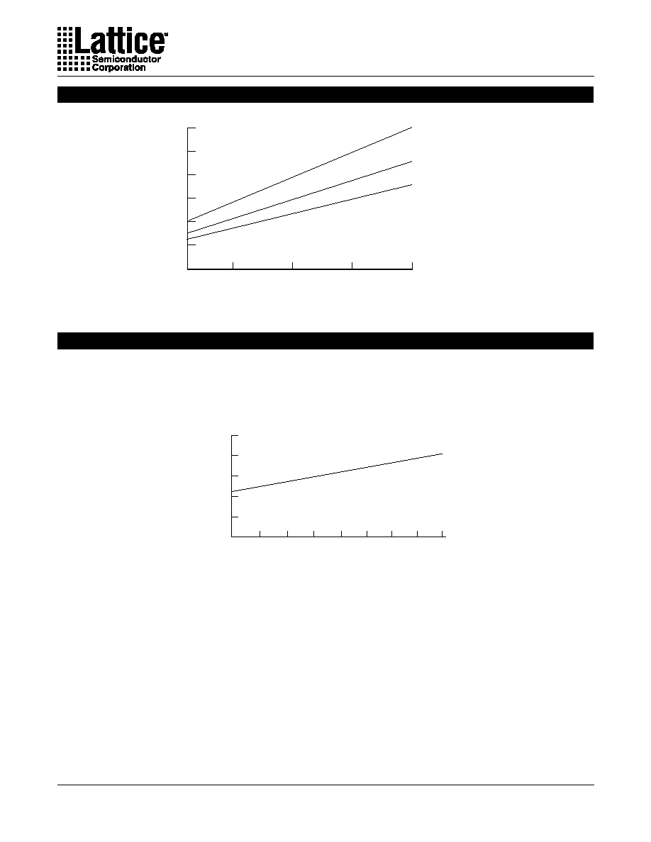
Maximum GRP Delay vs GLB Loads
ispLSI 1032-80
ispLSI 1032-60
ispLSI 1032-90
0126A-80-32-isp
1
2
3
4
8
12
16
GLB Loads
GRP Delay (ns)
4
5
6
0
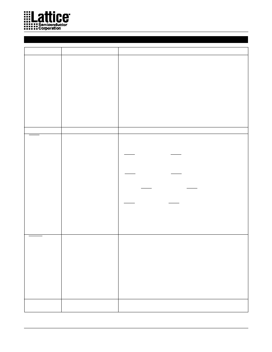
Power Consumption
ure 3 shows the relationship between power and operat-
ing speed.
Power consumption in the ispLSI 1032 device depends
on two primary factors: the speed at which the device is
operating, and the number of Product Terms used. Fig-
Figure 3. Typical Device Power Consumption vs fmax
50
100
150
200
250
0
10
20
30
40
50
60
70
f
max (MHz)
I
CC (mA)
80
Notes: Configuration of eight 16-bit Counters
Typical Current at 5V, 25þC
ispLSI 1032
0127A-32-80-isp
ICC can be estimated for the ispLSI 1032 using the following equation:
ICC = 52 + (# of PTs * 0.30) + (# of nets * Max. freq * 0.009) where:
# of PTs = Number of Product Terms used in design
# of nets = Number of Signals used in device
Max. freq = Highest Clock Frequency to the device
The ICC estimate is based on typical conditions (VCC = 5.0V, room temperature) and an assumption of 2 GLB loads on
average exists. These values are for estimates only. Since the value of ICC is sensitive to operating conditions and the
program in the device, the actual ICC should be verified.

Specifications
ispLSI 1032
10
Pin Description
Input -- Dedicated in-system programming enable input pin. This pin
is brought low to enable the programming mode. The MODE, SDI,
SDO and SCLK options become active.
Input --
This pin performs two functions. It is a dedicated input pin when
ispEN is logic high. When ispEN is logic low, it functions as an input
pin to load programming data into the device. SDI/IN 0 also is used as
one of the two control pins for the isp state machine.
Input --
This pin performs two functions. It is a dedicated input pin when
ispEN is logic high. When ispEN is logic low, it functions as a pin to
control the operation of the isp state machine.
Input/Output --
This pin performs two functions. It is a dedicated input
pin when ispEN is logic high. When ispEN is logic low, it functions as
an output pin to read serial shift register data.
Input -- This pin performs two functions. It is a dedicated input when
ispEN is logic high. When ispEN is logic low, it functions as a clock pin
for the Serial Shift Register.
Name
PLCC Pin Numbers
Description
Input/Output Pins - These are the general purpose I/O pins used by the
logic array.
I/O 0 - I/O 3
26,
27,
28,
29,
I/O 4 - I/O 7
30,
31,
32,
33,
I/O 8 - I/O 11
34,
35,
36,
37,
I/O 12 - I/O 15
38,
39,
40,
41,
I/O 16 - I/O 19
45,
46,
47,
48,
I/O 20 - I/O 23
49,
50,
51,
52,
I/O 24 - I/O 27
53,
54,
55,
56,
I/O 28 - I/O 31
57,
58,
59,
60,
I/O 32 - I/O 35
68,
69,
70,
71,
I/O 36 - I/O 39
72,
73,
74,
75,
I/O 40 - I/O 43
76,
77,
78,
79,
I/O 44 - I/O 47
80,
81,
82,
83,
I/O 48 - I/O 51
3,
4,
5,
6,
I/O 52 - I/O 55
7,
8,
9,
10,
I/O 56 - I/O 59
11,
12,
13,
14,
I/O 60 - I/O 63
15,
16,
17,
18
IN 4 - IN 7
67,
84,
2,
19
Dedicated input pins to the device.
Active Low (0) Reset pin which resets all of the GLB and I/O registers
in the device.
Dedicated Clock input. This clock input is connected to one of the
clock inputs of all of the GLBs on the device.
Dedicated Clock input. This clock input is brought into the clock
distribution network, and can optionally be routed to any GLB on the
device.
Dedicated Clock input. This clock input is brought into the clock
distribution network, and can optionally be routed to any GLB and/or
any I/O cell on the device.
Dedicated Clock input. This clock input is brought into the clock
distribution network, and can optionally be routed to any I/O cell on the
device.
ispEN
23
SDI/IN 0
1
25
MODE/IN 1
1
42
SDO/IN 2
1
44
SCLK/IN 3
1
61
GND
1,
22,
43,
64
V
CC
21,
65
Ground (GND)
V
CC
RESET
24
Y0
20
Y1
66
Y2
63
Y3
62
1. Pins have dual function capability
Specifications
ispLSI 1032
11
Pin Description
Input -- Dedicated in-system programming enable input pin. This pin
is brought low to enable the programming mode. The MODE, SDI,
SDO and SCLK options become active.
Input --
This pin performs two functions. It is a dedicated input pin when
ispEN is logic high. When ispEN is logic low, it functions as an input
pin to load programming data into the device. SDI/IN 0 also is used as
one of the two control pins for the isp state machine.
Input --
This pin performs two functions. It is a dedicated input pin when
ispEN is logic high. When ispEN is logic low, it functions as a pin to
control the operation of the isp state machine.
Input/Output --
This pin performs two functions. It is a dedicated input
pin when ispEN is logic high. When ispEN is logic low, it functions as
an output pin to read serial shift register data.
Input -- This pin performs two functions. It is a dedicated input when
ispEN is logic high. When ispEN is logic low, it functions as a clock pin
for the Serial Shift Register.
No Connect
Description
TQFP Pin Numbers
Name
Input/Output Pins - These are the general purpose I/O pins used by the
logic array.
I/O 0 - I/O 3
17,
18,
19,
20,
I/O 4 - I/O 7
21,
22,
23,
28,
I/O 8 - I/O 11
29,
30,
31,
32,
I/O 12 - I/O 15
33,
34,
35,
36,
I/O 16 - I/O 19
40,
41,
42,
43,
I/O 20 - I/O 23
44,
45,
46,
47,
I/O 24 - I/O 27
48,
53,
54,
55,
I/O 28 - I/O 31
56,
57,
58,
59,
I/O 32 - I/O 35
67,
68,
69,
70,
I/O 36 - I/O 39
71,
72,
73,
78,
I/O 40 - I/O 43
79,
80,
81,
82,
I/O 44 - I/O 47
83,
84,
85,
86,
I/O 48 - I/O 51
90,
91,
92,
93,
I/O 52 - I/O 55
94,
95,
96,
97,
I/O 56 - I/O 59
98,
3,
4,
5,
I/O 60 - I/O 63
6,
7,
8,
9
IN 4 - IN 7
66,
87,
89,
10
Dedicated input pins to the device.
ispEN
14
SDI/IN 0
1
16
MODE/IN 1
1
37
SDO/IN 2
1
39
SCLK/IN 3
1
60
NC
2
1,
2,
24,
25,
26,
27,
49,
50,
51,
52,
74,
75
76,
77,
99,
100
Active Low (0) Reset pin which resets all of the GLB and I/O registers
in the device.
Dedicated Clock input. This clock input is connected to one of the
clock inputs of all of the GLBs on the device.
Dedicated Clock input. This clock input is brought into the clock
distribution network, and can optionally be routed to any GLB on the
device.
Dedicated Clock input. This clock input is brought into the clock
distribution network, and can optionally be routed to any GLB and/or
any I/O cell on the device.
Dedicated Clock input. This clock input is brought into the clock
distribution network, and can optionally be routed to any I/O cell on the
device.
RESET
15
Y0
11
Y1
65
Y2
62
Y3
61
GND
13,
38,
63,
88
V
CC
12,
64
Ground (GND)
V
CC
1. Pins have dual function capability
2. NC pins are not to be connected to any active signals, Vcc or GND.

Specifications
ispLSI 1032
12
Pin Description
RESET
G1
Y0
E1
Y1
E11
Y2
G9
Y3
G11
NC
2
G3
GND
C6,
F3,
F9,
J6
V
CC
F2,
F11
I/O 0 - I/O 3
F1,
H1,
H2,
J1,
I/O 4 - I/O 7
K1,
J2,
L1,
K2,
I/O 8 - I/O 11
K3,
L2,
L3,
K4,
I/O 12 - I/O 15
L4,
J5,
K5,
L5,
I/O 16 - I/O 19
L7,
K7,
L6,
L8,
I/O 20 - I/O 23
K8,
L9,
L10,
K9,
I/O 24 - I/O 27
L11,
K10,
J10,
K11,
I/O 28 - I/O 31
J11,
H10, H11, F10,
I/O 32 - I/O 35
E9,
D11, D10, C11,
I/O 36 - I/O 39
B11,
C10, A11,
B10,
I/O 40 - I/O 43
B9,
A10,
A9,
B8,
I/O 44 - I/O 47
A8,
B6,
B7,
A7,
I/O 48 - I/O 51
A5,
B5,
C5,
A4,
I/O 52 - I/O 55
B4,
A3,
A2,
B3,
I/O 56 - I/O 59
A1,
B2,
C2,
B1,
I/O 60 - I/O 63
C1,
D2,
D1,
E3
IN 4 - IN 7
E10,
C7,
A6,
E2
Dedicated input pins to the device.
Input/Output Pins - These are the general purpose I/O pins used by the
logic array.
Name
CPGA Pin Numbers
Description
Input ≠ Dedicated in-system programming enable input pin. This pin
is brought low to enable the programming mode. The MODE, SDI,
SDO and SCLK options become active.
Input ≠ This pin performs two functions. It is a dedicated input pin when
ispEN is logic high. When ispEN is logic low, it functions as an input
pin to load programming data into the device. SDI/IN 0 also is used as
one of the two control pins for the isp state machine.
Input ≠ This pin performs two functions. It is a dedicated input pin when
ispEN is logic high. When ispEN is logic low, it functions as a pin to
control the operation of the isp state machine.
Input/Output ≠ This pin performs two functions. It is a dedicated input
pin when ispEN is logic high. When ispEN is logic low, it functions as
an output pin to read serial shift register data.
Input ≠ This pin performs two functions. It is a dedicated input when
ispEN is logic high. When ispEN is logic low, it functions as a clock pin
for the Serial Shift Register.
ispEN
G3
SDI/IN 0
1
G2
MODE/IN 1
1
K6
SDO/IN 2
1
J7
SCLK/IN 3
1
G10
Active Low (0) Reset pin which resets all of the GLB and I/O registers
in the device.
Dedicated Clock input. This clock input is connected to one of the
clock inputs of all of the GLBs on the device.
Dedicated Clock input. This clock input is brought into the clock
distribution network, and can optionally be routed to any GLB on the
device.
Dedicated Clock input. This clock input is brought into the clock
distribution network, and can optionally be routed to any GLB and/or
any I/O cell on the device.
Dedicated Clock input. This clock input is brought into the clock
distribution network, and can optionally be routed to any I/O cell on the
device.
No Connect
Ground (GND)
V
CC
Table 2-0002-32/883
1. Pins have dual function capability.
2. NC pins are not to be connected to any active signals, Vcc or GND.
Specifications
ispLSI 1032
13
Pin Configuration
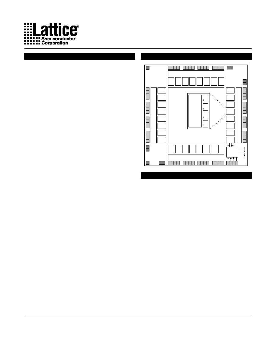
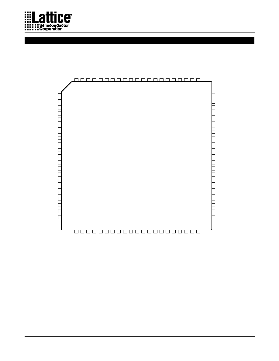
ispLSI 1032 84-Pin PLCC Pinout Diagram
I/O 38
I/O 37
I/O 36
I/O 35
I/O 34
I/O 33
I/O 32
IN 4
Y1
VCC
GND
Y2
Y3
IN 3/SCLK*
I/O 31
I/O 30
I/O 29
I/O 28
I/O 27
I/O 26
I/O 25
I/O 57
I/O 58
I/O 59
I/O 60
I/O 61
I/O 62
I/O 63
IN 7
Y0
VCC
GND
ispEN
RESET
*SDI/IN 0
I/O 0
I/O 1
I/O 2
I/O 3
I/O 4
I/O 5
I/O 6
I/O 56
I/O 55
I/O 54
I/O 53
I/O 52
I/O 51
I/O 50
I/O 49
I/O 48
IN 6
GND
IN 5
I/O 47
I/O 46
I/O 45
I/O 44
I/O 43
I/O 42
I/O 41
I/O 40
I/O 39
I/O 7
I/O 8
I/O 9
I/O 10
I/O 11
I/O 12
I/O 13
I/O 14
I/O 15
*MODE/IN 1
GND
*SDO/IN 2
I/O 16
I/O 17
I/O 18
I/O 19
I/O 20
I/O 21
I/O 22
I/O 23
I/O 24
11 10 9 8 7 6 5 4 3 2 1 84 83 82 81 80 79 78 77 76 75
12
13
14
15
16
17
18
19
20
21
22
23
24
25
26
27
28
29
30
31
32
74
73
72
71
70
69
68
67
66
65
64
63
62
61
60
59
58
57
56
55
54
33 34 35 36 37 38 39 40 41 42 43 44 45 46 47 48 49 50 51 52 53
ispLSI 1032
Top View
*Pins have dual function capability.
0123-32-isp
Specifications
ispLSI 1032
14
1NC
1NC
I/O 57
I/O 58
I/O 59
I/O 60
I/O 61
I/O 62
I/O 63
IN 7
Y0
VCC
GND
ispEN
RESET
2SDI/IN 0
I/O 0
I/O 1
I/O 2
I/O 3
I/O 4
I/O 5
I/O 6
1NC
1NC
NC1
NC1
I/O 38
I/O 37
I/O 36
I/O 35
I/O 34
I/O 33
I/O 32
IN 4
Y1
VCC
GND
Y2
Y3
IN 3/SCLK2
I/O 31
I/O 30
I/O 29
I/O 28
I/O 27
I/O 26
I/O 25
NC1
NC1
NC
1
NC
1
I/O 56
I/O 55
I/O 54
I/O 53
I/O 52
I/O 51
I/O 50
I/O 49
I/O 48
IN 6
GND
IN 5
I/O 47
I/O 46
I/O 45
I/O 44
I/O 43
I/O 42
I/O 41
I/O 40
I/O 39
NC
1
NC
1
1
NC
1
NC
I/O 7
I/O 8
I/O 9
I/O 10
I/O 11
I/O 12
I/O 13
I/O 14
I/O 15
2
MODE/IN1
GND
2
SDO/IN 2
I/O 16
I/O 17
I/O 18
I/O 19
I/O 20
I/O 21
I/O 22
I/O 23
I/O 24
1
NC
1
NC
1
2
3
4
5
6
7
8
9
10
11
12
13
14
15
16
17
18
19
20
21
22
23
24
25
75
74
73
72
71
70
69
68
67
66
65
64
63
62
61
60
59
57
56
55
54
53
52
51
26
27
28
29
30
31
32
33
34
35
36
37
38
39
40
41
42
43
44
45
46
47
48
49
50
100
99
98
97
96
95
94
93
92
91
90
89
88
87
86
85
84
83
82
81
80
79
78
77
76
58
ispLSI 1032
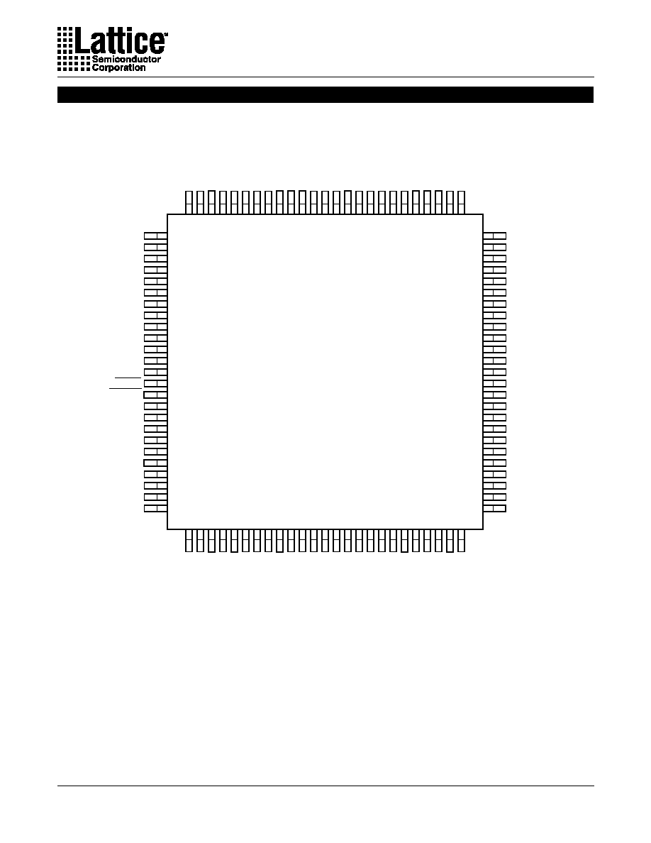
Top View
1. NC pins are not to be connected to any active signal, Vcc or GND.
2. Pins have dual function capability.
0766A-32-isp
Pin Configuration
ispLSI 1032 100-pin TQFP Pinout Diagram
Specifications
ispLSI 1032
15
I
/O38
I
/O36
I
/O35
I
/O33
Y1
Vcc
Y3
I
/O30
I
/O28
I
/O27
I
/O24
I
/O41
I
/O39
I
/O37
I
/O34
I
N4
I
/O31
*SCLK/
I
N3
I
/O29
I
/O26
I
/O25
I
/O22
I
/O42
I
/O40
I
/O32
GND
Y2
I
/O23
I
/O21
I
/O44
I
/O43
I
/O20
I
/O19
I
/O47
I
/O46
I
N5
*SDO/
I
N2
I
/O17
I
/O16
I
N6
I
/O45
GND
GND
*MODE/
I
N1
I
/O18
I
/O48
I
/O49
I
/O50
I
/O13
I
/O14
I
/O15
I
/O51
I
/O52
I
/O11
I
/O12
I
/O53
I
/O55
INDEX
I
/O63
GND
ispEN
I
/O8
I
/O10
I
/O54
I
/O57
I
/O58
I
/O61
I
N7
Vcc
*SDI/
I
N0
I
/O2
I
/O5
I
/O7
I
/O9
I
/O56
I
/O59
I
/O60
I
/O62
Y0
I
/O0
RESET
I
/O1
I
/O3
I
/O4
I
/O6
ispLSI 1032/883
Bottom View
A
B
C
D
E
F
G
H
J
K
L
11 10 9 8 7 6 5 4 3 2 1
PIN A1
*Pins have dual function capability.
0488A-32-isp/883
Pin Configuration
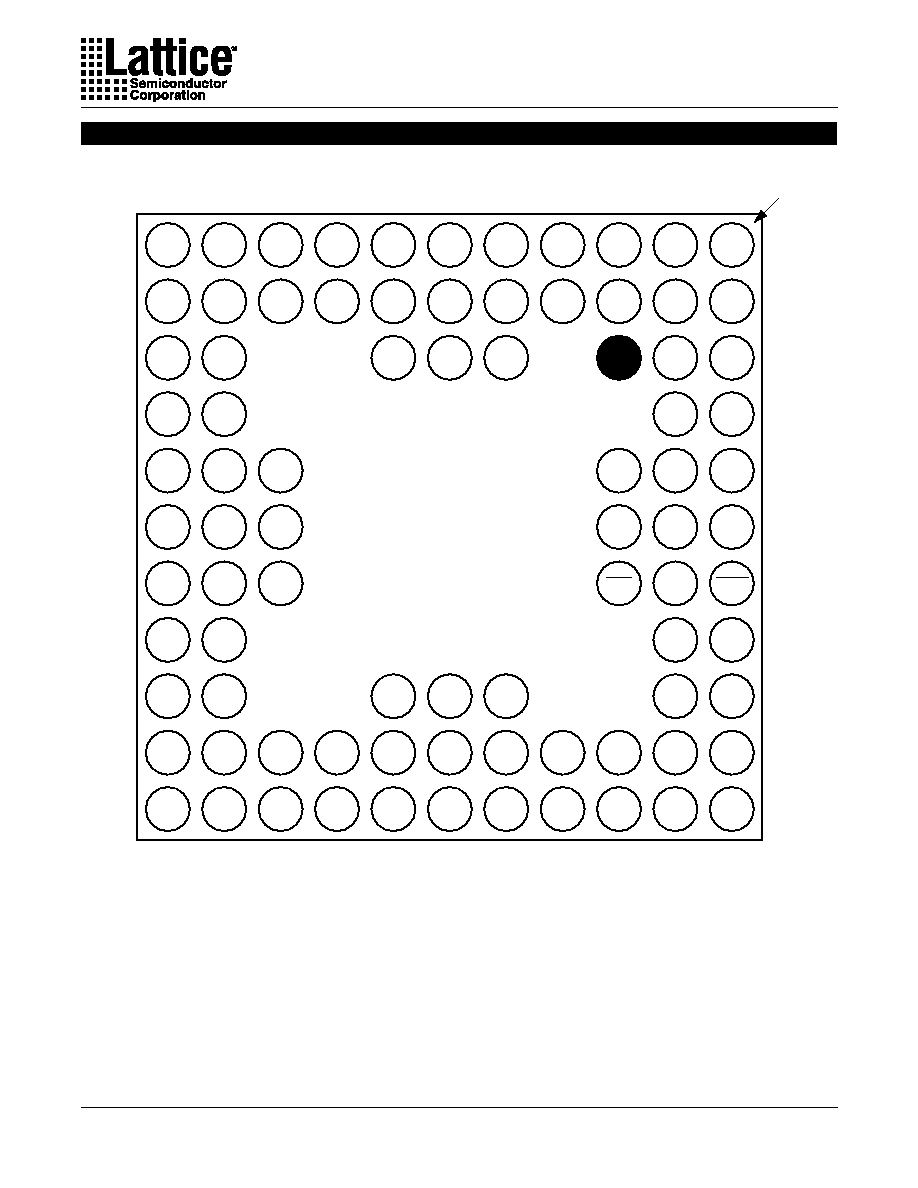
ispLSI 1032/883 84-Pin CPGA Pinout Diagram
Specifications
ispLSI 1032
16
USE ispLSI 1032E
FOR NEW COMMERCIAL &
INDUSTRIAL DESIGNS
t
pd (ns)
f
max (MHz)
Ordering Number
Package
90
12
ispLSI 1032-90LT
100-Pin TQFP
80
15
ispLSI 1032-80LJ
84-Pin PLCC
COMMERCIAL
90
12
ispLSI 1032-90LJ
84-Pin PLCC
80
15
ispLSI 1032-80LT
100-Pin TQFP
60
20
ispLSI 1032-60LJ
84-Pin PLCC
60
20
ispLSI 1032-60LT
100-Pin TQFP
INDUSTRIAL
t
pd (ns)
f
max (MHz)
Ordering Number
Package
60
20
ispLSI 1032-60LJI
84-Pin PLCC
Family
ispLSI
ispLSI
Family
Table 2- 0041A-32-isp
MILITARY/883
t
pd (ns)
f
max (MHz)
Ordering Number
Package
60
20
ispLSI 1032-60LG/883
84-Pin CPGA
ispLSI
Family
SMD Number
5962-9308501MXC
Note: Lattice Semiconductor recognizes the trend in military device procurement towards
using SMD compliant devices, as such, ordering by this number is recommended.
60
20
ispLSI 1032-60LTI
100-Pin TQFP
Ordering Information
Part Number Description
Device Number
Grade
Blank = Commercial
I = Industrial
/883 = 883 Military Process
1032
XX
X
X
X
Speed
90 = 90 MHz
f
max
80 = 80 MHz
f
max
60 = 60 MHz
f
max
Power
L = Low
Package
J = PLCC
T = TQFP
G = CPGA
--
Device Family
0212-80B-isp1032
ispLSI