Document Outline
- ispLSI 2032/A Data Sheet
- DC Electrical Characteristics
- AC Characteristics
- Pin Configuration: 44 PLCC
- Pin Configuration: 44 TQFP
- Pin Configuration: 48 TQFP
- Ordering Information

ispLSI
Æ
2032/A
In-System Programmable High Density PLD
2032_10
1
USE ispLSI 2032E FOR NEW DESIGNS
Features
∑ ENHANCEMENTS
-- ispLSI 2032A is Fully Form and Function Compatible
to the ispLSI 2032, with Identical Timing
Specifcations and Packaging
-- ispLSI 2032A is Built on an Advanced 0.35 Micron
E
2
CMOS
Æ
Technology
∑ HIGH DENSITY PROGRAMMABLE LOGIC
-- 1000 PLD Gates
-- 32 I/O Pins, Two Dedicated Inputs
-- 32 Registers
-- High Speed Global Interconnect
-- Wide Input Gating for Fast Counters, State
Machines, Address Decoders, etc.
-- Small Logic Block Size for Random Logic
∑ HIGH PERFORMANCE E
2
CMOS
Æ
TECHNOLOGY
--
f
max = 180 MHz Maximum Operating Frequency
--
t
pd = 5.0 ns Propagation Delay
-- TTL Compatible Inputs and Outputs
-- Electrically Erasable and Reprogrammable
-- Non-Volatile
-- 100% Tested at Time of Manufacture
-- Unused Product Term Shutdown Saves Power
∑ IN-SYSTEM PROGRAMMABLE
-- In-System Programmable (ISPTM) 5V Only
-- Increased Manufacturing Yields, Reduced Time-to-
Market and Improved Product Quality
-- Reprogram Soldered Devices for Faster Prototyping
∑ OFFERS THE EASE OF USE AND FAST SYSTEM
SPEED OF PLDs WITH THE DENSITY AND FLEXIBILITY
OF FIELD PROGRAMMABLE GATE ARRAYS
-- Complete Programmable Device Can Combine Glue
Logic and Structured Designs
-- Enhanced Pin Locking Capability
-- Three Dedicated Clock Input Pins
-- Synchronous and Asynchronous Clocks
-- Programmable Output Slew Rate Control to
Minimize Switching Noise
-- Flexible Pin Placement
-- Optimized Global Routing Pool Provides Global
Interconnectivity
Description
The ispLSI 2032 and 2032A are High Density Program-
mable Logic Devices. The devices contain 32 Registers,
32 Universal I/O pins, two Dedicated Input Pins, three
Dedicated Clock Input Pins, one dedicated Global OE
input pin and a Global Routing Pool (GRP). The GRP
provides complete interconnectivity between all of these
elements. The ispLSI 2032 and 2032A feature 5V in-
system programmability and in-system diagnostic
capabilities. The ispLSI 2032 and 2032A offer non-
volatile reprogrammability of the logic, as well as the
interconnect to provide truly reconfigurable systems.
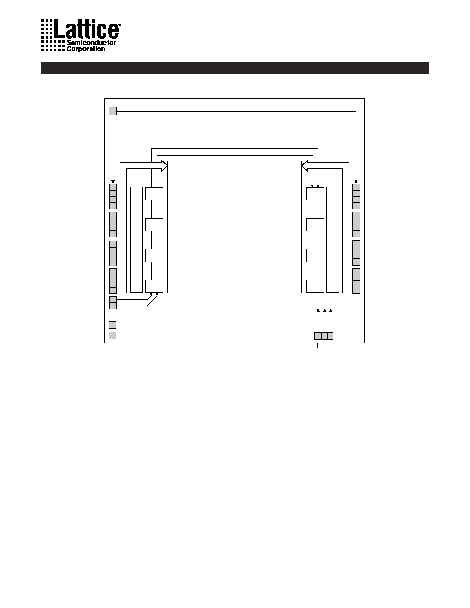
The basic unit of logic on these devices is the Generic
Logic Block (GLB). The GLBs are labeled A0, A1 .. A7
(Figure 1). There are a total of eight GLBs in the ispLSI
2032 and 2032A devices. Each GLB is made up of four
macrocells. Each GLB has 18 inputs, a programmable
AND/OR/Exclusive OR array, and four outputs which can
be configured to be either combinatorial or registered.
Inputs to the GLB come from the GRP and dedicated
inputs. All of the GLB outputs are brought back into the
GRP so that they can be connected to the inputs of any
GLB on the device.
Functional Block Diagram
Global Routing Pool
(GRP)
A0
A1
A3
Input Bus
Output Routing Pool (ORP)
A7
A6
A5
A4
Input Bus
Output Routing Pool (ORP)
A2
GLB
Logic
Array
D Q
D Q
D Q
D Q
0139Bisp/2000
Copyright © 2002 Lattice Semiconductor Corp. All brand or product names are trademarks or registered trademarks of their respective holders. The specifications and information herein are subject
to change without notice.
LATTICE SEMICONDUCTOR CORP., 5555 Northeast Moore Ct., Hillsboro, Oregon 97124, U.S.A.
Tel. (503) 268-8000; 1-800-LATTICE; FAX (503) 268-8556; http://www.latticesemi.com
January 2002

Specifications
ispLSI 2032/A
2
USE ispLSI 2032E FOR NEW DESIGNS
Functional Block Diagram
Figure 1. ispLSI 2032/A Functional Block Diagram
Global Routing Pool
(GRP)
A0
A1
A3
Input Bus
Output Routing Pool (ORP)
A7
A6
A5
A4
Input Bus
Output Routing Pool (ORP)
A2
CLK 0
CLK 1
CLK 2
GOE 0
Notes:
*Y1 and RESET are multiplexed on the same pin
I/O 0
I/O 1
I/O 2
I/O 3
I/O 6
I/O 7
I/O 8
I/O 9
I/O 10
I/O 11
I/O 12
I/O 13
I/O 14
I/O 15
I/O 31
I/O 30
I/O 29
I/O 28
I/O 27
I/O 26
I/O 25
I/O 24
I/O 23
I/O 22
I/O 21
I/O 20
I/O 19
I/O 18
I/O 17
I/O 16
SDI/IN 0
SDO/IN 1
I/O 4
I/O 5
Y0
*Y1/
RESET
SCLK/Y2
ispEN
MODE
0139B(1)isp/2000
The devices also have 32 I/O cells, each of which is
directly connected to an I/O pin. Each I/O cell can be
individually programmed to be a combinatorial input,
output or bi-directional I/O pin with 3-state control. The
signal levels are TTL compatible voltages and the output
drivers can source 4 mA or sink 8 mA. Each output can
be programmed independently for fast or slow output
slew rate to minimize overall output switching noise.
Eight GLBs, 32 I/O cells, two dedicated inputs and two
ORPs are connected together to make a Megablock
(Figure 1). The outputs of the eight GLBs are connected
to a set of 32 universal I/O cells by the ORP. Each ispLSI
2032 and 2032A device contains one Megablock.
The GRP has as its inputs, the outputs from all of the
GLBs and all of the inputs from the bi-directional I/O cells.
All of these signals are made available to the inputs of the
GLBs. Delays through the GRP have been equalized to
minimize timing skew.
Clocks in the ispLSI 2032 and 2032A devices are se-
lected using the dedicated clock pins. Three dedicated
clock pins (Y0, Y1, Y2) or an asynchronous clock can be
selected on a GLB basis. The asynchronous or Product
Term clock can be generated in any GLB for its own clock.

Specifications
ispLSI 2032/A
3
USE ispLSI 2032E FOR NEW DESIGNS
Absolute Maximum Ratings
1
Supply Voltage V
cc
...................................-0.5 to +7.0V
Input Voltage Applied ........................ -2.5 to V
CC
+1.0V
Off-State Output Voltage Applied ..... -2.5 to V
CC
+1.0V
Storage Temperature ................................ -65 to 150
∞
C
Case Temp. with Power Applied .............. -55 to 125
∞
C
Max. Junction Temp. (T
J
) with Power Applied ... 150
∞
C
1. Stresses above those listed under the "Absolute Maximum Ratings" may cause permanent damage to the device. Functional
operation of the device at these or at any other conditions above those indicated in the operational sections of this specification
is not implied (while programming, follow the programming specifications).
DC Recommended Operating Condition
T
A
= 0
∞
C to + 70
∞
C
T
A
= -40
∞
C to + 85
∞
C
SYMBOL
Table 2 - 0005/2032
V
CC
V
IH
V
IL
PARAMETER
Supply Voltage
Input High Voltage
Input Low Voltage
MIN.
MAX.
UNITS
4.75
4.5
2.0
0
5.25
5.5
V
cc
+1
0.8
V
V
V
V
Commercial
Industrial
Capacitance (T
A
=25
∞
C, f=1.0 MHz)
C
SYMBOL
Table 2-0006/2032
C
PARAMETER
I/O Capacitance
7
UNITS
TYPICAL
TEST CONDITIONS
1
2
6
Dedicated Input Capacitance
pf
pf
V = 5.0V, V = 2.0V
V = 5.0V, V = 2.0V
CC
CC
I/O
IN
C
Clock Capacitance
10
3
pf
V = 5.0V, V = 2.0V
CC
Y
Data Retention Specifications
Table 2-0008A-isp
PARAMETER
Data Retention
MINIMUM
MAXIMUM
UNITS
Erase/Reprogram Cycles
20
10000
≠
≠
Years
Cycles

Specifications
ispLSI 2032/A
4
USE ispLSI 2032E FOR NEW DESIGNS
Input Pulse Levels
Table 2-0003/2032
Input Rise and Fall Time
10% to 90%
Input Timing Reference Levels
Output Timing Reference Levels
Output Load
GND to 3.0V
1.5V
1.5V
See Figure 2
3-state levels are measured 0.5V from
steady-state active level.
-135, -150, -180
-80, -110
1.5 ns
3 ns
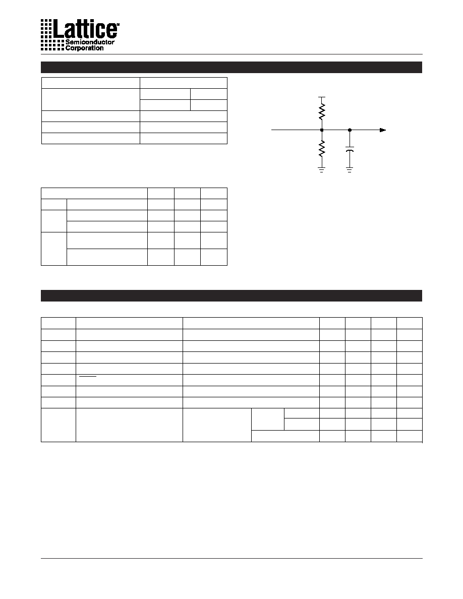
Figure 2. Test Load
+ 5V
R1
R2
CL
*
Device
Output
Test
Point
*
CL includes Test Fixture and Probe Capacitance.
0213A
Switching Test Conditions
DC Electrical Characteristics
Over Recommended Operating Conditions
Output Load Conditions (see Figure 2)
TEST CONDITION
R1
R2
CL
A
470
390
35pF
B
390
35pF
470
390
35pF
Active High
Active Low
C
470
390
5pF
390
5pF
Active Low to Z
at V +0.5V
OL
Active High to Z
at V -0.5V
OH
Table 2 - 0004A
V
OL
SYMBOL
1. One output at a time for a maximum duration of one second. V = 0.5V was selected to avoid test problems
by tester ground degradation. Characterized but not 100% tested.
2. Measured using two 16-bit counters.
3. Typical values are at V = 5V and T = 25
∞
C.
4. Maximum I varies widely with specific device configuration and operating frequency. Refer to the Power Consumption
section of this data sheet and Thermal Management section of the Lattice Semiconductor Data Book or CD-ROM to
estimate maximum I .
Table 2-0007/2032
1
V
OH
I
IH
I
IL
I
IL-isp
PARAMETER
I
IL-PU
I
OS
2, 4
I
CC
Output Low Voltage
Output High Voltage
Input or I/O High Leakage Current
Input or I/O Low Leakage Current
ispEN Input Low Leakage Current
I/O Active Pull-Up Current
Output Short Circuit Current
Operating Power Supply Current
I = 8 mA
I = -4 mA
3.5V
V
V
0V
V
V (Max.)
0V
V
V
0V
V
V
V = 5V, V = 0.5V
V = 0.0V, V = 3.0V
f = 1 MHz
OL
OH
IN IL
IN CC
IN
IL
IN IL
CC OUT
TOGGLE
IL IH
CONDITION
MIN.
TYP.
MAX. UNITS
3
≠
2.4
≠
≠
≠
≠
≠
≠
≠
≠
≠
≠
≠
≠
0.4
≠
10
-10
-150
-150
-200
V
V
µ
A
µ
A
µ
A
µ
A
mA
CC
A
OUT
≠
≠
40
40
mA
mA
≠
≠
≠
60
mA
≠
-180, -150
Others
CC
CC
Comm.
Industrial

Specifications
ispLSI 2032/A
5
USE ispLSI 2032E FOR NEW DESIGNS
External Timing Parameters
Over Recommended Operating Conditions
t
pd1
UNITS
-150
MIN.
TEST
COND.
1. Unless noted otherwise, all parameters use the GRP, 20 PTXOR path, ORP and Y0 clock.
2. Refer to Timing Model in this data sheet for further details.
3. Standard 16-bit counter using GRP feedback.
4. Reference Switching Test Conditions section.
Table 2-0030B-180/2032
1
4
3
1
tsu2 + tco1
( )
-135
MIN.
MAX.
MAX.
DESCRIPTION
#
2
PARAMETER
A
1
Data Prop. Delay, 4PT Bypass, ORP Bypass
≠
5.5
≠
7.5
ns
t
pd2
A
2
Data Prop. Delay
≠
≠
ns
f
max
A
3
Clk Frequency with Internal Feedback
154
≠
137
≠
MHz
f
max (Ext.)
≠
4
Clk Frequency with Ext. Feedback
≠
≠
MHz
f
max (Tog.)
≠
5
Clk Frequency, Max. Toggle
≠
≠
MHz
t
su1
≠
6
GLB Reg Setup Time before Clk, 4 PT Bypass
≠
≠
ns
t
co1
A
7
GLB Reg. Clk to Output Delay, ORP Bypass
≠
≠
ns
t
h1
≠
8
GLB Reg. Hold Time after Clk, 4 PT Bypass
0.0
≠
ns
t
su2
≠
9
GLB Reg. Setup Time before Clk
4.5
≠
ns
t
co2
≠
10 GLB Reg. Clk to Output Delay
≠
≠
ns
t
h2
≠
11 GLB Reg. Hold Time after Clk
0.0
≠
ns
t
r1
A
12 Ext. Reset Pin to Output Delay
≠
≠
ns
t
rw1
≠
13 Ext. Reset Pulse Duration
4.5
≠
ns
t
ptoeen
B
14 Input to Output Enable
≠
≠
ns
t
ptoedis
C
15 Input to Output Disable
≠
≠
ns
t
goeen
B
16 Global OE Output Enable
≠
≠
ns
t
goedis
C
17 Global OE Output Disable
≠
≠
ns
t
wh
≠
18 Ext. Synchronous Clk Pulse Duration, High
3.0
≠
≠
ns
t
wl
≠
19 Ext. Synchronous Clk Pulse Duration, Low
3.0
≠
≠
ns
111
167
3.0
4.5
≠
≠
5.0
≠
8.0
≠
11.0
11.0
5.0
5.0
8.0
-180
MIN. MAX.
≠
5.0
≠
180
≠
≠
≠
≠
≠
0.0
4.0
≠
0.0
≠
4.0
≠
≠
≠
≠
2.5
≠
2.5
≠
125
200
3.0
4.0
≠
≠
4.5
≠
7.0
≠
10.0
10.0
5.0
5.0
7.5
100
167
4.0
0.0
5.5
0.0
5.0
3.0
3.0
10.0
4.5
5.5
10.0
12.0
12.0
6.0
6.0


