Document Outline
- Features
- ispMACH 4000 Introduction
- Overview
- ispMACH 4000 Architecture
- I/O Cell
- Global OE Generation
- Zero Power/Low Power and Power Management
- IEEE 1149.1-Compliant Boundary Scan Testability
- I/O Quick Configuration
- IEEE 1532-Compliant In-System Programming
- Security Bit
- Hot Socketing
- Density Migration
- Absolute Maximum Ratings1, 2, 3
- Recommended Operating Conditions
- Erase Reprogram Specifications
- Hot Socketing Characteristics1,2,3
- I/O Recommended Operating Conditions
- DC Electrical Characteristics
- Supply Current, ispMACH 4000V/B/C�
- Supply Current, ispMACH 4000Z�
- I/O DC Electrical Characteristics
- ispMACH 4000V/B/C External Switching Characteristics
- ispMACH 4000V/B/C External Switching Characteristics (Cont.)
- ispMACH 4000Z External Switching Characteristics
- ispMACH 4000Z External Switching Characteristics (Cont.)
- Timing Model
- ispMACH 4000V/B/C Internal Timing Parameters�
- ispMACH 4000V/B/C Internal Timing Parameters�
- ispMACH 4000Z Internal Timing Parameters�
- ispMACH 4000Z Internal Timing Parameters (Cont.)
- ispMACH 4000V/B/C Timing Adders1
- ispMACH 4000V/B/C Timing Adders1 (Cont.)
- ispMACH 4000Z Timing Adders�1
- ispMACH 4000Z Timing Adders (Cont.)1
- Boundary Scan Waveforms and Timing Specifications
- Power Consumption
- Power Estimation Coefficients1
- Switching Test Conditions
- Signal Descriptions
- ispMACH 4000V/B/C ORP Reference Table
- ispMACH 4000Z ORP Reference Table
- ispMACH 4000V/B/C/Z Power Supply and NC Connections1
- ispMACH 4000V/B/C/Z Power Supply and NC Connections1 (Cont.)
- ispMACH 4032V/B/C and 4064V/B/C Logic Signal Connections: 44-Pin TQFP�
- ispMACH 4032V/B/C/Z and 4064V/B/C/Z Logic Signal Connections: 48-Pin TQFP�
- ispMACH 4032Z and 4064Z Logic Signal Connections: 56-Ball csBGA�
- ispMACH 4064V/B/C/Z, 4128V/B/C/Z, 4256V/B/C/Z Logic Signal Connections: 100-Pin TQFP�
- ispMACH 4128V/B/C Logic Signal Connections: 128-Pin TQFP�
- ispMACH 4064Z, 4128Z and 4256Z Logic Signal Connections: 132-Ball csBGA�
- ispMACH 4128V and 4256V Logic Signal Connections: 144-Pin TQFP�
- ispMACH 4256V/B/C/Z, 4384V/B/C, 4512V/B/C, Logic Signal Connections: 176-Pin TQFP�
- ispMACH 4256V/B/C, 4384V/B/C, 4512V/B/C Logic Signal Connections: 256-Ball fpBGA�
- Part Number Description
- ispMACH 4000 Family Speed Grade Offering
- Ordering Information
- For Further Information


Lattice Semiconductor
ispMACH 4000V/B/C/Z Family Data Sheet
3
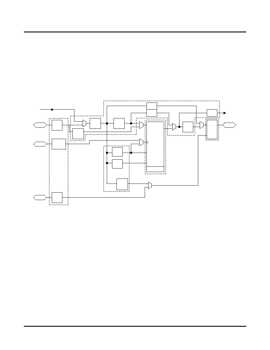
Figure 1. Functional Block Diagram
The I/Os in the ispMACH 4000 are split into two banks. Each bank has a separate I/O power supply. Inputs can
support a variety of standards independent of the chip or bank power supply. Outputs support the standards com-
patible with the power supply provided to the bank. Support for a variety of standards helps designers implement
designs in mixed voltage environments. In addition, 5V tolerant inputs are specified within an I/O bank that is con-
nected to V
CCO
of 3.0V to 3.6V for LVCMOS 3.3, LVTTL and PCI interfaces.
ispMACH 4000 Architecture
There are a total of two GLBs in the ispMACH 4032, increasing to 32 GLBs in the ispMACH 4512. Each GLB has
36 inputs. All GLB inputs come from the GRP and all outputs from the GLB are brought back into the GRP to be
connected to the inputs of any other GLB on the device. Even if feedback signals return to the same GLB, they still
must go through the GRP. This mechanism ensures that GLBs communicate with each other with consistent and
predictable delays. The outputs from the GLB are also sent to the ORP. The ORP then sends them to the associ-
ated I/O cells in the I/O block.
Generic Logic Block
The ispMACH 4000 GLB consists of a programmable AND array, logic allocator, 16 macrocells and a GLB clock
generator. Macrocells are decoupled from the product terms through the logic allocator and the I/O pins are decou-
pled from macrocells through the ORP. Figure 2 illustrates the GLB.
I/O
Block
ORP
ORP
16
16
GOE0
GOE1
V
CC
GND
TCK
TMS
TDI
TDO
36
Generic
Logic
Block
Generic
Logic
Block
I/O
Block
ORP
ORP
16
36
Generic
Logic
Block
Generic
Logic
Block
I/O
Block
I/O Bank 0
I/O Bank 1
I/O
Block
36
36
CLK0/I
CLK1/I
CLK2/I
CLK3/I
16
16
Global Routing P
ool
V
CCO0
GND
V
CCO1
GND
16
16
16

Lattice Semiconductor
ispMACH 4000V/B/C/Z Family Data Sheet
4
Figure 2. Generic Logic Block
AND Array
The programmable AND Array consists of 36 inputs and 83 output product terms. The 36 inputs from the GRP are
used to form 72 lines in the AND Array (true and complement of the inputs). Each line in the array can be con-
nected to any of the 83 output product terms via a wired-AND. Each of the 80 logic product terms feed the logic
allocator with the remaining three control product terms feeding the Shared PT Clock, Shared PT Initialization and
Shared PT OE. The Shared PT Clock and Shared PT Initialization signals can optionally be inverted before being
fed to the macrocells.
Every set of five product terms from the 80 logic product terms forms a product term cluster starting with PT0.
There is one product term cluster for every macrocell in the GLB. Figure 3 is a graphical representation of the AND
Array.
Logic Allocator
36 Inputs
from GRP
16 Macrocells
To ORP
To GRP
To
Product Term
Output Enable
Sharing
1+OE
16 MC Feedback Signals
Clock
Generator
1+OE
1+OE
1+OE
1+OE
1+OE
1+OE
CLK0
CLK1
CLK2
CLK3
1+OE
AND Array
36 Inputs,
83 Product Terms

Lattice Semiconductor
ispMACH 4000V/B/C/Z Family Data Sheet
5
Figure 3. AND Array
Enhanced Logic Allocator
Within the logic allocator, product terms are allocated to macrocells in product term clusters. Each product term
cluster is associated with a macrocell. The cluster size for the ispMACH 4000 family is 4+1 (total 5) product terms.
The software automatically considers the availability and distribution of product term clusters as it fits the functions
within a GLB. The logic allocator is designed to provide three speed paths: 5-PT fast bypass path, 20-PT Speed
Locking path and an up to 80-PT path. The availability of these three paths lets designers trade timing variability for
increased performance.
The enhanced Logic Allocator of the ispMACH 4000 family consists of the following blocks:
� Product Term Allocator
� Cluster Allocator
� Wide Steering Logic
Figure 4 shows a macrocell slice of the Logic Allocator. There are 16 such slices in the GLB.
Figure 4. Macrocell Slice
PT0
PT1
Cluster 0
PT2
PT3
PT4
In[0]
In[34]
In[35]
Note:
Indicates programmable fuse.
PT80
PT81
PT82
Shared PT Clock
Shared PT Initialization
Shared PTOE
PT76
PT77
PT78
PT79
PT75
Cluster 15
to
n+1
to
n-1
to
n-2
from
n-1
from
n-4
from
n+2
from
n+1
5-PT
From
n-4
1-80
PTs
To n+4
Fast 5-PT
Path
To XOR (MC)
Cluster
Individual Product
Term Allocator
Cluster
Allocator
SuperWIDETM
Steering Logic
n

Lattice Semiconductor
ispMACH 4000V/B/C/Z Family Data Sheet
6
Product Term Allocator
The product term allocator assigns product terms from a cluster to either logic or control applications as required
by the design being implemented. Product terms that are used as logic are steered into a 5-input OR gate associ-
ated with the cluster. Product terms that used for control are steered either to the macrocell or I/O cell associated
with the cluster. Table 3 shows the available functions for each of the five product terms in the cluster. The OR gate
output connects to the associated I/O cell, providing a fast path for narrow combinatorial functions, and to the logic
allocator.
Table 3. Individual PT Steering
Cluster Allocator
The cluster allocator allows clusters to be steered to neighboring macrocells, thus allowing the creation of functions
with more product terms. Table 4 shows which clusters can be steered to which macrocells. Used in this manner,
the cluster allocator can be used to form functions of up to 20 product terms. Additionally, the cluster allocator
accepts inputs from the wide steering logic. Using these inputs, functions up to 80 product terms can be created.
Table 4. Available Clusters for Each Macrocell
Wide Steering Logic
The wide steering logic allows the output of the cluster allocator n to be connected to the input of the cluster alloca-
tor
n
+4. Thus, cluster chains can be formed with up to 80 product terms, supporting wide product term functions
and allowing performance to be increased through a single GLB implementation. Table 5 shows the product term
chains.
Product Term
Logic
Control
PT
n
Logic PT
Single PT for XOR/OR
PT
n
+1
Logic PT
Individual Clock (PT Clock)
PT
n
+2
Logic PT
Individual Initialization or Individual Clock Enable (PT Initialization/CE)
PT
n
+3
Logic PT
Individual Initialization (PT Initialization)
PT
n
+4
Logic PT
Individual OE (PTOE)
Macrocell
Available Clusters
M0
--
C0
C1
C2
M1
C0
C1
C2
C3
M2
C1
C2
C3
C4
M3
C2
C3
C4
C5
M4
C3
C4
C5
C6
M5
C4
C5
C6
C7
M6
C5
C6
C7
C8
M7
C6
C7
C8
C9
M8
C7
C8
C9
C10
M9
C8
C9
C10
C11
M10
C9
C10
C11
C12
M11
C10
C11
C12
C13
M12
C11
C12
C13
C14
M13
C12
C13
C14
C15
M14
C13
C14
C15
--
M15
C14
C15
--
--
Lattice Semiconductor
ispMACH 4000V/B/C/Z Family Data Sheet
7
Table 5. Product Term Expansion Capability
Every time the super cluster allocator is used, there is an incremental delay of t
EXP
. When the super cluster alloca-
tor is used, all destinations other than the one being steered to, are given the value of ground (i.e., if the super clus-
ter is steered to M (n+4), then M (n) is ground).
Macrocell
The 16 macrocells in the GLB are driven by the 16 outputs from the logic allocator. Each macrocell contains a pro-
grammable XOR gate, a programmable register/latch, along with routing for the logic and control functions.
Figure 5 shows a graphical representation of the macrocell. The macrocells feed the ORP and GRP. A direct input
from the I/O cell allows designers to use the macrocell to construct high-speed input registers. A programmable
delay in this path allows designers to choose between the fastest possible set-up time and zero hold time.
Figure 5. Macrocell
Enhanced Clock Multiplexer
The clock input to the flip-flop can select any of the four block clocks along with the shared PT clock, and true and
complement forms of the optional individual term clock. An 8:1 multiplexer structure is used to select the clock. The
eight sources for the clock multiplexer are as follows:
� Block CLK0
� Block CLK1
Expansion
Chains
Macrocells Associated with Expansion Chain
(with Wrap Around)
Max PT/
Macrocell
Chain-0
M0
M4
M8
M12
M0
75
Chain-1
M1
M5
M9
M13
M1
80
Chain-2
M2
M6
M10
M14
M2
75
Chain-3
M3
M7
M11
M15
M3
70
Single PT
Block CLK0
Block CLK1
Block CLK2
Block CLK3
PT Clock (optional)
Shared PT Clock
CE
D/T/L
Q
R
P
Shared PT Initialization
PT Initialization/CE (optional)
PT Initialization (optional)
From Logic Allocator
Power-up
Initialization
To ORP
To GRP
From I/O Cell
Delay

Lattice Semiconductor
ispMACH 4000V/B/C/Z Family Data Sheet
8
� Block CLK2
� Block CLK3
� PT Clock
� PT Clock Inverted
� Shared PT Clock
� Ground
Clock Enable Multiplexer
Each macrocell has a 4:1 clock enable multiplexer. This allows the clock enable signal to be selected from the fol-
lowing four sources:
� PT Initialization/CE
� PT Initialization/CE Inverted
� Shared PT Clock
� Logic High
Initialization Control
The ispMACH 4000 family architecture accommodates both block-level and macrocell-level set and reset capability.
There is one block-level initialization term that is distributed to all macrocell registers in a GLB. At the macrocell
level, two product terms can be "stolen" from the cluster associated with a macrocell to be used for set/reset func-
tionality. A reset/preset swapping feature in each macrocell allows for reset and preset to be exchanged, providing
flexibility.
Note that the reset/preset swapping selection feature affects power-up reset as well. All flip-flops power up to a
known state for predictable system initialization. If a macrocell is configured to SET on a signal from the block-level
initialization, then that macrocell will be SET during device power-up. If a macrocell is configured to RESET on a
signal from the block-level initialization or is not configured for set/reset, then that macrocell will RESET on power-
up. To guarantee initialization values, the V
CC
rise must be monotonic, and the clock must be inactive until the reset
delay time has elapsed.
GLB Clock Generator
Each ispMACH 4000 device has up to four clock pins that are also routed to the GRP to be used as inputs. These
pins drive a clock generator in each GLB, as shown in Figure 6. The clock generator provides four clock signals that
can be used anywhere in the GLB. These four GLB clock signals can consist of a number of combinations of the
true and complement edges of the global clock signals.
Figure 6. GLB Clock Generator
CLK0
CLK1
CLK2
CLK3
Block CLK0
Block CLK1
Block CLK2
Block CLK3

Lattice Semiconductor
ispMACH 4000V/B/C/Z Family Data Sheet
9
Output Routing Pool (ORP)
The Output Routing Pool allows macrocell outputs to be connected to any of several I/O cells within an I/O block.
This provides greater flexibility in determining the pinout and allows design changes to occur without affecting the
pinout. The output routing pool also provides a parallel capability for routing macrocell-level OE product terms. This
allows the OE product term to follow the macrocell output as it is switched between I/O cells. Additionally, the out-
put routing pool allows the macrocell output or true and complement forms of the 5-PT bypass signal to bypass the
output routing multipliers and feed the I/O cell directly. The enhanced ORP of the ispMACH 4000 family consists of
the following elements:
� Output Routing Multiplexers
� OE Routing Multiplexers
� Output Routing Pool Bypass Multiplexers
Figure 7 shows the structure of the ORP from the I/O cell perspective. This is referred to as an ORP slice. Each
ORP has as many ORP slices as there are I/O cells in the corresponding I/O block.
Figure 7. ORP Slice
Output Routing Multiplexers
The details of connections between the macrocells and the I/O cells vary across devices and within a device
dependent on the maximum number of I/Os available. Tables 5-9 provide the connection details.
Table 6. ORP Combinations for I/O Blocks with 8 I/Os
I/O Cell
Available Macrocells
I/O 0
M0, M1, M2, M3, M4, M5, M6, M7
I/O 1
M2, M3, M4, M5, M6, M7, M8, M9
I/O 2
M4, M5, M6, M7, M8, M9, M10, M11
I/O 3
M6, M7, M8, M9, M10, M11, M12, M13
I/O 4
M8, M9, M10, M11, M12, M13, M14, M15
I/O 5
M10, M11, M12, M13, M14, M15, M0, M1
I/O 6
M12, M13, M14, M15, M0, M1, M2, M3
I/O 7
M14, M15, M0, M1, M2, M3, M4, M5
Output Routing Multiplexer
OE Routing Multiplexer
ORP
Bypass
Multiplexer
From Macrocell
From PTOE
To I/O
Cell
To I/O
Cell
Output
OE
5-PT Fast Path
Lattice Semiconductor
ispMACH 4000V/B/C/Z Family Data Sheet
10
Table 7. ORP Combinations for I/O Blocks with 16 I/Os
Table 8. ORP Combinations for I/O Blocks with 4 I/Os
Table 9. ORP Combinations for I/O Blocks with 10 I/Os
I/O Cell
Available Macrocells
I/O 0
M0, M1, M2, M3, M4, M5, M6, M7
I/O 1
M1, M2, M3, M4, M5, M6, M7, M8
I/O 2
M2, M3, M4, M5, M6, M7, M8, M9
I/O 3
M3, M4, M5, M6, M7, M8, M9, M10
I/O 4
M4, M5, M6, M7, M8, M9, M10, M11
I/O 5
M5, M6, M7, M8, M9, M10, M11, M12
I/O 6
M6, M7, M8, M9, M10, M11, M12, M13
I/O 7
M7, M8, M9, M10, M11, M12, M13, M14
I/O 8
M8, M9, M10, M11, M12, M13, M14, M15
I/O 9
M9, M10, M11, M12, M13, M14, M15, M0
I/O 10
M10, M11, M12, M13, M14, M15, M0, M1
I/O 11
M11, M12, M13, M14, M15, M0, M1, M2
I/O 12
M12, M13, M14, M15, M0, M1, M2, M3
I/O 13
M13, M14, M15, M0, M1, M2, M3, M4
I/O 14
M14, M15, M0, M1, M2, M3, M4, M5
I/O 15
M15, M0, M1, M2, M3, M4, M5, M6
I/O Cell
Available Macrocells
I/O 0
M0, M1, M2, M3, M4, M5, M6, M7
I/O 1
M4, M5, M6, M7, M8, M9, M10, M11
I/O 2
M8, M9, M10, M11, M12, M13, M14, M15
I/O 3
M12, M13, M14, M15, M0, M1, M2, M3
I/O Cell
Available Macrocells
I/O 0
M0, M1, M2, M3, M4, M5, M6, M7
I/O 1
M2, M3, M4, M5, M6, M7, M8, M9
I/O 2
M4, M5, M6, M7, M8, M9, M10, M11
I/O 3
M6, M7, M8, M9, M10, M11, M12, M13
I/O 4
M8, M9, M10, M11, M12, M13, M14, M15
I/O 5
M10, M11, M12, M13, M14, M15, M0, M1
I/O 6
M12, M13, M14, M15, M0, M1, M2, M3
I/O 7
M14, M15, M0, M1, M2, M3, M4, M5
I/O 8
M2, M3, M4, M5, M6, M7, M8, M9
I/O 9
M10, M11, M12, M13, M14, M15, M0, M1

Lattice Semiconductor
ispMACH 4000V/B/C/Z Family Data Sheet
11
Table 10. ORP Combinations for I/O Blocks with 12 I/Os
ORP Bypass and Fast Output Multiplexers
The ORP bypass and fast-path output multiplexer is a 4:1 multiplexer and allows the 5-PT fast path to bypass the
ORP and be connected directly to the pin with either the regular output or the inverted output. This multiplexer also
allows the register output to bypass the ORP to achieve faster t
CO
.
Output Enable Routing Multiplexers
The OE Routing Pool provides the corresponding local output enable (OE) product term to the I/O cell.
I/O Cell
The I/O cell contains the following programmable elements: output buffer, input buffer, OE multiplexer and bus
maintenance circuitry. Figure 8 details the I/O cell.
Figure 8. I/O Cell
Each output supports a variety of output standards dependent on the V
CCO
supplied to its I/O bank. Outputs can
also be configured for open drain operation. Each input can be programmed to support a variety of standards, inde-
pendent of the V
CCO
supplied to its I/O bank. The I/O standards supported are:
I/O Cell
Available Macrocells
I/O 0
M0, M1, M2, M3, M4, M5, M6, M7
I/O 1
M1, M2, M3, M4, M5, M6, M7, M8
I/O 2
M2, M3, M4, M5, M6, M7, M8, M9
I/O 3
M4, M5, M6, M7, M8, M9, M10, M11
I/O 4
M5, M6, M7, M8, M9, M10, M11, M12
I/O 5
M6, M7, M8, M9, M10, M11, M12, M13
I/O 6
M8, M9, M10, M11, M12, M13, M14, M15
I/O 7
M9, M10, M11, M12, M13, M14, M15, M0
I/O 8
M10, M11, M12, M13, M14, M15, M0, M1
I/O 9
M12, M13, M14, M15, M0, M1, M2, M3
I/O 10
M13, M14, M15, M0, M1, M2, M3, M4
I/O 11
M14, M15, M0, M1, M2, M3, M4, M5
GOE 0
From ORP
*Global fuses
From ORP
To Macrocell
To GRP
GOE 1
GOE 2
GOE 3
VCC
V
CCO
V
CCO
*
*
*

Lattice Semiconductor
ispMACH 4000V/B/C/Z Family Data Sheet
12
� LVTTL
� LVCMOS 1.8
� LVCMOS 3.3
� 3.3V PCI Compatible
� LVCMOS 2.5
All of the I/Os and dedicated inputs have the capability to provide a bus-keeper latch, Pull-up Resistor or Pull-down
Resistor. A fourth option is to provide none of these. The selection is done on a global basis. The default in both
hardware and software is such that when the device is erased or if the user does not specify, the input structure is
configured to be a Pull-up Resistor.
Each ispMACH 4000 device I/O has an individually programmable output slew rate control bit. Each output can be
individually configured for fast slew or slow slew. The typical edge rate difference between fast and slow slew set-
ting is 20%. For high-speed designs with long, unterminated traces, the slow-slew rate will introduce fewer reflec-
tions, less noise and keep ground bounce to a minimum. For designs with short traces or well terminated lines, the
fast slew rate can be used to achieve the highest speed.
Global OE Generation
Most ispMACH 4000 family devices have a 4-bit wide Global OE Bus, except the ispMACH 4032 device that has a
2-bit wide Global OE Bus. This bus is derived from a 4-bit internal global OE PT bus and two dual purpose I/O or
GOE pins. Each signal that drives the bus can optionally be inverted.
Each GLB has a block-level OE PT that connects to all bits of the Global OE PT bus with four fuses. Hence, for a
256-macrocell device (with 16 blocks), each line of the bus is driven from 16 OE product terms. Figures 9 and 10
show a graphical representation of the global OE generation.
Figure 9. Global OE Generation for All Devices Except ispMACH 4032
Shared PTOE
(Block 0)
Shared PTOE
(Block n)
Global
Fuses
GOE (0:3)
to I/O cells
Internal Global OE
PT Bus
(4 lines)
4-Bit
Global OE Bus
Global OE
Fuse connection
Hard wired

Lattice Semiconductor
ispMACH 4000V/B/C/Z Family Data Sheet
13
Figure 10. Global OE Generation for ispMACH 4032
Zero Power/Low Power and Power Management
The ispMACH 4000 family is designed with high speed low power design techniques to offer both high speed and
low power. With an advanced E
2
low power cell and non sense-amplifier design approach (full CMOS logic
approach), the ispMACH 4000 family offers SuperFAST pin-to-pin speeds, while simultaneously delivering low
standby power without needing any "turbo bits" or other power management schemes associated with a traditional
sense-amplifier approach.
The zero power ispMACH 4000Z is based on the 1.8V ispMACH 4000C family. With innovative circuit design
changes, the ispMACH 4000Z family is able to achieve the industry's "lowest static power".
IEEE 1149.1-Compliant Boundary Scan Testability
All ispMACH 4000 devices have boundary scan cells and are compliant to the IEEE 1149.1 standard. This allows
functional testing of the circuit board on which the device is mounted through a serial scan path that can access all
critical logic notes. Internal registers are linked internally, allowing test data to be shifted in and loaded directly onto
test nodes, or test node data to be captured and shifted out for verification. In addition, these devices can be linked
into a board-level serial scan path for more board-level testing. The test access port operates with an LVCMOS
interface that corresponds to the power supply voltage.
I/O Quick Configuration
To facilitate the most efficient board test, the physical nature of the I/O cells must be set before running any continu-
ity tests. As these tests are fast, by nature, the overhead and time that is required for configuration of the I/Os'
physical nature should be minimal so that board test time is minimized. The ispMACH 4000 family of devices allows
this by offering the user the ability to quickly configure the physical nature of the I/O cells. This quick configuration
takes milliseconds to complete, whereas it takes seconds for the entire device to be programmed. Lattice's
ispVMTM System programming software can either perform the quick configuration through the PC parallel port, or
can generate the ATE or test vectors necessary for a third-party test system.
Shared PTOE
(Block 0)
Shared PTOE
(Block 1)
Global
Fuses
GOE (3:0)
to I/O cells
Internal Global OE
PT Bus
(2 lines)
4-Bit
Global OE Bus
Global OE
Fuse connection
Hard wired

Lattice Semiconductor
ispMACH 4000V/B/C/Z Family Data Sheet
14
IEEE 1532-Compliant In-System Programming
Programming devices in-system provides a number of significant benefits including: rapid prototyping, lower inven-
tory levels, higher quality and the ability to make in-field modifications. All ispMACH 4000 devices provide In-Sys-
tem Programming (ISPTM) capability through the Boundary Scan Test Access Port. This capability has been
implemented in a manner that ensures that the port remains complaint to the IEEE 1149.1 standard. By using IEEE
1149.1 as the communication interface through which ISP is achieved, users get the benefit of a standard, well-
defined interface. All ispMACH 4000 devices are also compliant with the IEEE 1532 standard.
The ispMACH 4000 devices can be programmed across the commercial temperature and voltage range. The PC-
based Lattice software facilitates in-system programming of ispMACH 4000 devices. The software takes the
JEDEC file output produced by the design implementation software, along with information about the scan chain,
and creates a set of vectors used to drive the scan chain. The software can use these vectors to drive a scan chain
via the parallel port of a PC. Alternatively, the software can output files in formats understood by common auto-
mated test equipment. This equipment can then be used to program ispMACH 4000 devices during the testing of a
circuit board.
Security Bit
A programmable security bit is provided on the ispMACH 4000 devices as a deterrent to unauthorized copying of
the array configuration patterns. Once programmed, this bit defeats readback of the programmed pattern by a
device programmer, securing proprietary designs from competitors. Programming and verification are also
defeated by the security bit. The bit can only be reset by erasing the entire device.
Hot Socketing
The ispMACH 4000 devices are well-suited for applications that require hot socketing capability. Hot socketing a
device requires that the device, during power-up and down, can tolerate active signals on the I/Os and inputs with-
out being damaged. Additionally, it requires that the effects of I/O pin loading be minimal on active signals. The
ispMACH 4000 devices provide this capability for input voltages in the range 0V to 3.0V.
Density Migration
The ispMACH 4000 family has been designed to ensure that different density devices in the same package have
the same pin-out. Furthermore, the architecture ensures a high success rate when performing design migration
from lower density parts to higher density parts. In many cases, it is possible to shift a lower utilization design tar-
geted for a high density device to a lower density device. However, the exact details of the final resource utilization
will impact the likely success in each case.
Lattice Semiconductor
ispMACH 4000V/B/C/Z Family Data Sheet
15
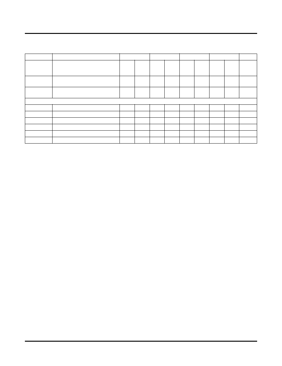
Absolute Maximum Ratings
1, 2, 3
ispMACH 4000C/Z
ispMACH 4000B
ispMACH 4000V
(1.8V)
(2.5V)
(3.3V)
Supply Voltage (V
CC
) . . . . . . . . . . . . . . . . . . . . . . -0.5 to 2.5V . . . . . . . . . .-0.5 to 5.5V. . . . . . . . . . . -0.5 to 5.5V
Output Supply Voltage (V
CCO
) . . . . . . . . . . . . . . . -0.5 to 4.5V . . . . . . . . . .-0.5 to 4.5V. . . . . . . . . . . -0.5 to 4.5V
Input or I/O Tristate Voltage Applied
4, 5
. . . . . . . . . -0.5 to 5.5V . . . . . . . . . .-0.5 to 5.5V. . . . . . . . . . . -0.5 to 5.5V
Storage Temperature . . . . . . . . . . . . . . . . . . . . . . -65 to 150
�
C. . . . . . . . . -65 to 150
�
C . . . . . . . . . .-65 to 150
�
C
Junction Temperature (T
j
) with Power Applied . . . -55 to 150�C. . . . . . . . . -55 to 150�C . . . . . . . . . .-55 to 150�C
1. Stress above those listed under the "Absolute Maximum Ratings" may cause permanent damage to the device. Functional
operation of the device at these or any other conditions above those indicated in the operational sections of this specification
is not implied.
2. Compliance with Lattice Thermal Management document is required.
3. All voltages referenced to GND.
4. Undershoot of -2V and overshoot of (V
IH
(MAX) + 2V), up to a total pin voltage of 6.0V, is permitted for a duration of < 20ns.
5. Maximum of 64 I/Os per device with VIN > 3.6V is allowed.
Recommended Operating Conditions
Erase Reprogram Specifications
Hot Socketing Characteristics
1,2,3
Symbol
Parameter
Min.
Max.
Units
V
CC
Supply Voltage for 1.8V Devices
ispMACH 4000C
1.65
1.95
V
ispMACH 4000Z
1.7
1.9
V
ispMACH 4000Z, Extended Functional Voltage
Operation
1.6
1, 2
1.9
V
Supply Voltage for 2.5V Devices
2.3
2.7
V
Supply Voltage for 3.3V Devices
3.0
3.6
V
T
j
Junction Temperature (Commercial)
0
90
C
Junction Temperature (Industrial)
-40
105
C
Junction Temperature (Automotive)
-40
130
C
1. Devices operating at 1.6V can expect performance degradation up to 35%.
2. Applicable for devices with 2004 datecodes and later. Contact factory for ordering instructions.
Parameter
Min.
Max.
Units
Erase/Reprogram Cycle
1,000
--
Cycles
Note: Valid over commercial temperature range.
Symbol
Parameter
Condition
Min.
Typ.
Max.
Units
I
DK
Input or I/O Leakage Current
0 V
IN
3.0V, Tj = 105�C
--
�30
�150
�A
0 V
IN
3.0V, Tj = 130�C
--
�30
�200
�A
1. Insensitive to sequence of V
CC
or V
CCO.
However, assumes monotonic rise/fall rates for V
CC
and V
CCO,
provided (V
IN
- V
CCO
) 3.6V.
2. 0 < V
CC
< V
CC
(MAX), 0 < V
CCO
< V
CCO
(MAX).
3. I
DK
is additive to I
PU
, I
PD
or I
BH
. Device defaults to pull-up until fuse circuitry is active.

Lattice Semiconductor
ispMACH 4000V/B/C/Z Family Data Sheet
16
I/O Recommended Operating Conditions
DC Electrical Characteristics
Over Recommended Operating Conditions
Standard
V
CCO
(V)
1
Min.
Max.
LVTTL
3.0
3.6
LVCMOS 3.3
3.0
3.6
Extended LVCMOS 3.3
2
2.7
3.6
LVCMOS 2.5
2.3
2.7
LVCMOS 1.8
1.65
1.95
PCI 3.3
3.0
3.6
1. Typical values for V
CCO
are the average of the min. and max. values.
2. ispMACH 4000Z only.
Symbol
Parameter
Condition
Min.
Typ.
Max.
Units
I
IL
, I
IH
1
Input Leakage Current (ispMACH
4000Z)
0 V
IN
V
CCO
--
0.5
1
�A
I
IH
1
Input High Leakage Current
(ispMACH 4000Z)
V
CCO
< V
IN
5.5V
--
--
10
�A
I
IL
, I
IH
1
Input Leakage Current (ispMACH
4000V/B/C)
0 V
IN
3.6V, T
j
= 105�C
--
--
10
�A
0 V
IN
3.6V, T
j
= 130�C
--
--
15
�A
I
IH
1,2
Input High Leakage Current
(ispMACH 4000V/B/C)
3.6V < V
IN
5.5V, T
j
= 105�C
3.0V V
CCO
3.6V
--
--
20
�A
3.6V < V
IN
5.5V, T
j
= 130�C
3.0V V
CCO
3.6V
--
--
50
�A
I
PU
I/O Weak Pull-up Resistor Current
0 V
IN
0.7V
CCO
-30
--
-150
�A
I
PD
I/O Weak Pull-down Resistor Current V
IL
(MAX) V
IN
V
IH
(MIN)
30
--
150
�A
I
BHLS
Bus Hold Low Sustaining Current
V
IN
= V
IL
(MAX)
30
--
--
�A
I
BHHS
Bus Hold High Sustaining Current
V
IN
= 0.7 V
CCO
-30
--
--
�A
I
BHLO
Bus Hold Low Overdrive Current
0V V
IN
V
BHT
--
--
150
�A
I
BHHO
Bus Hold High Overdrive Current
V
BHT
V
IN
V
CCO
--
--
-150
�A
V
BHT
Bus Hold Trip Points
--
V
CCO
* 0.35
--
V
CCO
* 0.65
V
C
1
I/O Capacitance
3
V
CCO
= 3.3V, 2.5V, 1.8V
--
8
--
pf
V
CC
= 1.8V, V
IO
= 0 to V
IH
(MAX)
--
--
C
2
Clock Capacitance
3
V
CCO
= 3.3V, 2.5V, 1.8V
--
6
--
pf
V
CC
= 1.8V, V
IO
= 0 to V
IH
(MAX)
--
--
C
3
Global Input Capacitance
3
V
CCO
= 3.3V, 2.5V, 1.8V
--
6
--
pf
V
CC
= 1.8V, V
IO
= 0 to V
IH
(MAX)
--
--
1. Input or I/O leakage current is measured with the pin configured as an input or as an I/O with the output driver tristated. It is not
measured with the output driver active. Bus maintenance circuits are disabled.
2. 5V tolerant inputs and I/O should only be placed in banks where 3.0V V
CCO
3.6V.
3. T
A
= 25�C, f = 1.0MHz
Lattice Semiconductor
ispMACH 4000V/B/C/Z Family Data Sheet
17
Supply Current, ispMACH 4000V/B/C
Over Recommended Operating Conditions
Symbol
Parameter
Condition
Min.
Typ.
Max.
Units
ispMACH 4032V/B/C
ICC
1,2,3
Operating Power Supply Current
Vcc = 3.3V
--
11.8
--
mA
Vcc = 2.5V
--
11.8
--
mA
Vcc = 1.8V
--
1.8
--
mA
ICC
4
Standby Power Supply Current
Vcc = 3.3V
--
11.3
--
mA
Vcc = 2.5V
--
11.3
--
mA
Vcc = 1.8V
--
1.3
--
mA
ispMACH 4064V/B/C
ICC
1,2,3
Operating Power Supply Current
Vcc = 3.3V
--
12
--
mA
Vcc = 2.5V
--
12
--
mA
Vcc = 1.8V
--
2
--
mA
ICC
5
Standby Power Supply Current
Vcc = 3.3V
--
11.5
--
mA
Vcc = 2.5V
--
11.5
--
mA
Vcc = 1.8V
--
1.5
--
mA
ispMACH 4128V/B/C
ICC
1,2,3
Operating Power Supply Current
Vcc = 3.3V
--
12
--
mA
Vcc = 2.5V
--
12
--
mA
Vcc = 1.8V
--
2
--
mA
ICC
4
Standby Power Supply Current
Vcc = 3.3V
--
11.5
--
mA
Vcc = 2.5V
--
11.5
--
mA
Vcc = 1.8V
--
1.5
--
mA
ispMACH 4256V/B/C
I
CC
1,2,3
Operating Power Supply Current
Vcc = 3.3V
--
12.5
--
mA
Vcc = 2.5V
--
12.5
--
mA
Vcc = 1.8V
--
2.5
--
mA
I
CC
4
Standby Power Supply Current
Vcc = 3.3V
--
12
--
mA
Vcc = 2.5V
--
12
--
mA
Vcc = 1.8V
--
2
--
mA
ispMACH 4384V/B/C
I
CC
1,2,3
Operating Power Supply Current
Vcc = 3.3V
--
13.5
--
mA
Vcc = 2.5V
--
13.5
--
mA
Vcc = 1.8V
--
3.5
--
mA
I
CC
4
Standby Power Supply Current
Vcc = 3.3V
--
12.5
--
mA
Vcc = 2.5V
--
12.5
--
mA
Vcc = 1.8V
--
2.5
--
mA
ispMACH 4512V/B/C
I
CC
1,2,3
Operating Power Supply Current
Vcc = 3.3V
--
14
--
mA
Vcc = 2.5V
--
14
--
mA
Vcc = 1.8V
--
4
--
mA

Lattice Semiconductor
ispMACH 4000V/B/C/Z Family Data Sheet
18
I
CC
4
Standby Power Supply Current
Vcc = 3.3V
--
13
--
mA
Vcc = 2.5V
--
13
--
mA
Vcc = 1.8V
--
3
--
mA
1. T
A
= 25�C, frequency = 1.0 MHz.
2. Device configured with 16-bit counters.
3. I
CC
varies with specific device configuration and operating frequency.
4. T
A
= 25�C
Supply Current, ispMACH 4000Z
Over Recommended Operating Conditions
Symbol
Parameter
Condition
Min.
Typ.
Max. Units
ispMACH 4032ZC
ICC
1, 2, 3, 5
Operating Power Supply Current
Vcc = 1.8V, T
A
= 25�C
--
50
--
�A
Vcc = 1.9V, T
A
= 70�C
--
58
--
�A
Vcc = 1.9V, T
A
= 85�C
--
60
--
�A
Vcc = 1.9V, T
A
= 125�C
--
70
--
�A
ICC
4, 5
Standby Power Supply Current
Vcc = 1.8V, T
A
= 25�C
--
10
--
�A
Vcc = 1.9V, T
A
= 70�C
--
13
20
�A
Vcc = 1.9V, T
A
= 85�C
--
15
25
�A
Vcc = 1.9V, T
A
= 125�C
--
22
--
�A
ispMACH 4064ZC
ICC
1, 2, 3, 5
Operating Power Supply Current
Vcc = 1.8V, T
A
= 25�C
--
80
--
�A
Vcc = 1.9V, T
A
= 70�C
--
89
--
�A
Vcc = 1.9V, T
A
= 85�C
--
92
--
�A
Vcc = 1.9V, T
A
= 125�C
--
109
--
�A
ICC
4, 5
Standby Power Supply Current
Vcc = 1.8V, T
A
= 25�C
--
11
--
�A
Vcc = 1.9V, T
A
= 70�C
--
15
25
�A
Vcc = 1.9V, T
A
= 85�C
--
18
35
�A
Vcc = 1.9V, T
A
= 125�C
--
37
--
�A
ispMACH 4128ZC
ICC
1, 2, 3, 5
Operating Power Supply Current
Vcc = 1.8V, T
A
= 25�C
--
168
--
�A
Vcc = 1.9V, T
A
= 70�C
--
190
--
�A
Vcc = 1.9V, T
A
= 85�C
--
195
--
�A
Vcc = 1.9V, T
A
= 125�C
--
212
--
�A
ICC
4, 5
Standby Power Supply Current
Vcc = 1.8V, T
A
= 25�C
--
12
--
�A
Vcc = 1.9V, T
A
= 70�C
--
16
35
�A
Vcc = 1.9V, T
A
= 85�C
--
19
50
�A
Vcc = 1.9V, T
A
= 125�C
--
42
--
�A
Supply Current, ispMACH 4000V/B/C (Cont.)
Over Recommended Operating Conditions
Symbol
Parameter
Condition
Min.
Typ.
Max.
Units

Lattice Semiconductor
ispMACH 4000V/B/C/Z Family Data Sheet
19
ispMACH 4256ZC
ICC
1, 2, 3, 5
Operating Power Supply Current
Vcc = 1.8V, T
A
= 25�C
--
341
--
�A
Vcc = 1.9V, T
A
= 70�C
--
361
--
�A
Vcc = 1.9V, T
A
= 85�C
--
372
--
�A
Vcc = 1.9V, T
A
= 125�C
--
468
--
�A
ICC
4, 5
Standby Power Supply Current
Vcc = 1.8V, T
A
= 25�C
--
13
--
�A
Vcc = 1.9V, T
A
= 70�C
--
32
55
�A
Vcc = 1.9V, T
A
= 85�C
--
43
90
�A
Vcc = 1.9V, T
A
= 125�C
--
135
--
�A
1. T
A
= 25�C, frequency = 1.0 MHz.
2. Device configured with 16-bit counters.
3. I
CC
varies with specific device configuration and operating frequency.
4. V
CCO
= 3.6V, V
IN
= 0V or V
CCO,
bus maintenance turned off. V
IN
above V
CCO
will add transient current above the specified standby I
CC
.
5. Includes V
CCO
current without output loading.
Supply Current, ispMACH 4000Z (Cont.)
Over Recommended Operating Conditions
Symbol
Parameter
Condition
Min.
Typ.
Max. Units

Lattice Semiconductor
ispMACH 4000V/B/C/Z Family Data Sheet
20
I/O DC Electrical Characteristics
Over Recommended Operating Conditions
Standard
V
IL
V
IH
V
OL
Max (V)
V
OH
Min (V)
I
OL
1
(mA)
I
OH
1
(mA)
Min (V)
Max (V)
Min (V)
Max (V)
LVTTL
-0.3
0.80
2.0
5.5
0.40
V
CCO
- 0.40
8.0
-4.0
0.20
V
CCO
- 0.20
0.1
-0.1
LVCMOS 3.3
-0.3
0.80
2.0
5.5
0.40
V
CCO
- 0.40
8.0
-4.0
0.20
V
CCO
- 0.20
0.1
-0.1
LVCMOS 2.5
-0.3
0.70
1.70
3.6
0.40
V
CCO
- 0.40
8.0
-4.0
0.20
V
CCO
- 0.20
0.1
-0.1
LVCMOS 1.8
(4000V/B)
-0.3
0.63
1.17
3.6
0.40
V
CCO
- 0.45
2.0
-2.0
0.20
V
CCO
- 0.20
0.1
-0.1
LVCMOS 1.8
(4000C/Z)
-0.3
0.35 * V
CC
0.65 * V
CC
3.6
0.40
V
CCO
- 0.45
2.0
-2.0
0.20
V
CCO
- 0.20
0.1
-0.1
PCI 3.3 (4000V/B)
-0.3
1.08
1.5
5.5
0.1 V
CCO
0.9 V
CCO
1.5
-0.5
PCI 3.3 (4000C/Z)
-0.3
0.3 * 3.3 * (V
CC
/
1.8) 0.5 * 3.3 * (V
CC
/
1.8)
5.5
0.1 V
CCO
0.9 V
CCO
1.5
-0.5
1. The average DC current drawn by I/Os between adjacent bank GND connections, or between the last GND in an I/O bank and the end of
the I/O bank, as shown in the logic signals connection table, shall not exceed n*8mA. Where n is the number of I/Os between bank GND
connections or between the last GND in a bank and the end of a bank.

Lattice Semiconductor
ispMACH 4000V/B/C/Z Family Data Sheet
21
V
O
Output Voltage (V)
Typical I/O Output Current (mA)
3.3V V
CCO
V
O
Output Voltage (V)
0
0
0
20
40
60
80
100
10
20
30
40
50
60
0
10
20
30
40
50
60
70
2.0
1.5
1.0
0.5
0
2.0 2.5
3.0 3.5
1.5
1.0
0.5
0
2.0
2.5
1.5
1.0
0.5
Typical I/O Output Current (mA)
1.8V V
CCO
V
O
Output Voltage (V)
I
OH
Typical I/O Output Current (mA)
2.5V V
CCO
I
OL
I
OH
I
OL
I
OH
I
OL

Lattice Semiconductor
ispMACH 4000V/B/C/Z Family Data Sheet
22
ispMACH 4000V/B/C External Switching Characteristics
Over Recommended Operating Conditions
Parameter
Description
1, 2, 3
-25
-27
-3
-35
Units
Min.
Max.
Min.
Max.
Min.
Max.
Min.
Max.
t
PD
5-PT bypass combinatorial propagation
delay
--
2.5
--
2.7
--
3.0
--
3.5
ns
t
PD_MC
20-PT combinatorial propagation delay
through macrocell
--
3.2
--
3.5
--
3.8
--
4.2
ns
t
S
GLB register setup time before clock
1.8
--
1.8
--
2.0
--
2.0
--
ns
t
ST
GLB register setup time before clock
with T-type register
2.0
--
2.0
--
2.2
--
2.2
--
ns
t
SIR
GLB register setup time before clock,
input register path
0.7
--
1.0
--
1.0
--
1.0
--
ns
t
SIRZ
GLB register setup time before clock
with zero hold
1.7
--
2.0
--
2.0
--
2.0
--
ns
t
H
GLB register hold time after clock
0.0
--
0.0
--
0.0
--
0.0
--
ns
t
HT
GLB register hold time after clock with
T-type register
0.0
--
0.0
--
0.0
--
0.0
--
ns
t
HIR
GLB register hold time after clock, input
register path
0.9
--
1.0
--
1.0
--
1.0
--
ns
t
HIRZ
GLB register hold time after clock, input
register path with zero hold
0.0
--
0.0
--
0.0
--
0.0
--
ns
t
CO
GLB register clock-to-output delay
--
2.2
--
2.7
--
2.7
--
2.7
ns
t
R
External reset pin to output delay
--
3.5
--
4.0
--
4.4
--
4.5
ns
t
RW
External reset pulse duration
1.5
--
1.5
--
1.5
--
1.5
-
ns
t
PTOE/DIS
Input to output local product term output
enable/disable
--
4.0
--
4.5
--
5.0
--
5.5
ns
t
GPTOE/DIS
Input to output global product term
output enable/disable
--
5.0
--
6.5
--
8.0
--
8.0
ns
t
GOE/DIS
Global OE input to output enable/disable
--
3.0
--
3.5
--
4.0
--
4.5
ns
t
CW
Global clock width, high or low
1.1
--
1.3
--
1.3
--
1.3
--
ns
t
GW
Global gate width low (for low
transparent) or high (for high transparent)
1.1
--
1.3
--
1.3
--
1.3
--
ns
t
WIR
Input register clock width, high or low
1.1
--
1.3
--
1.3
--
1.3
--
ns
f
MAX
4
Clock frequency with internal feedback
400
--
333
--
322
--
322
--
MHz
f
MAX
(Ext.)
Clock frequency with external feedback,
[1/ (t
S
+ t
CO
)]
250
--
222
--
212
--
212
--
MHz
1. Timing numbers are based on default LVCMOS 1.8 I/O buffers. Use timing adjusters provided to calculate other standards.
Timing v.3.2
2. Measured using standard switching circuit, assuming GRP loading of 1 and 1 output switching.
3. Pulse widths and clock widths less than minimum will cause unknown behavior.
4. Standard 16-bit counter using GRP feedback.

Lattice Semiconductor
ispMACH 4000V/B/C/Z Family Data Sheet
23
ispMACH 4000V/B/C External Switching Characteristics (Cont.)
Over Recommended Operating Conditions
Parameter
Description
1, 2, 3
-5
-75
-10
Units
Min.
Max.
Min.
Max.
Min.
Max.
t
PD
5-PT bypass combinatorial propagation delay
--
5.0
--
7.5
--
10.0
ns
t
PD_MC
20-PT combinatorial propagation delay through macrocell
--
5.5
--
8.0
--
10.5
ns
t
S
GLB register setup time before clock
3.0
--
4.5
--
5.5
--
ns
t
ST
GLB register setup time before clock with T-type register
3.2
--
4.7
--
5.5
--
ns
t
SIR
GLB register setup time before clock, input register path
1.2
--
1.7
--
1.7
--
ns
t
SIRZ
GLB register setup time before clock with zero hold
2.2
--
2.7
--
2.7
--
ns
t
H
GLB register hold time after clock
0.0
--
0.0
--
0.0
--
ns
t
HT
GLB register hold time after clock with T-type register
0.0
--
0.0
--
0.0
--
ns
t
HIR
GLB register hold time after clock, input register path
1.0
--
1.0
--
1.0
--
ns
t
HIRZ
GLB register hold time after clock, input register path with
zero hold
0.0
--
0.0
--
0.0
--
ns
t
CO
GLB register clock-to-output delay
--
3.4
--
4.5
--
6.0
ns
t
R
External reset pin to output delay
--
6.3
--
9.0
--
10.5
ns
t
RW
External reset pulse duration
2.0
--
4.0
--
4.0
--
ns
t
PTOE/DIS
Input to output local product term output enable/disable
--
7.0
--
9.0
--
10.5
ns
t
GPTOE/DIS
Input to output global product term output enable/disable
--
9.0
--
10.3
--
12.0
ns
t
GOE/DIS
Global OE input to output enable/disable
--
5.0
--
7.0
--
8.0
ns
t
CW
Global clock width, high or low
2.2
--
3.3
--
4.0
--
ns
t
GW
Global gate width low (for low transparent) or high (for
high transparent)
2.2
--
3.3
--
4.0
--
ns
t
WIR
Input register clock width, high or low
2.2
--
3.3
--
4.0
--
ns
f
MAX
4
Clock frequency with internal feedback
227
--
168
--
125
--
MHz
f
MAX
(Ext.) Clock frequency with external feedback, [1/ (t
S
+ t
CO
)]
156
--
111
--
86
--
MHz
1. Timing numbers are based on default LVCMOS 1.8 I/O buffers. Use timing adjusters provided to calculate other standards.
Timing v.3.2
2. Measured using standard switching circuit, assuming GRP loading of 1 and 1 output switching.
3. Pulse widths and clock widths less than minimum will cause unknown behavior.
4. Standard 16-bit counter using GRP feedback.

Lattice Semiconductor
ispMACH 4000V/B/C/Z Family Data Sheet
24
ispMACH 4000Z External Switching Characteristics
Over Recommended Operating Conditions
Parameter
Description
1, 2, 3
-35
-37
-42
Units
Min.
Max.
Min.
Max.
Min.
Max.
t
PD
5-PT bypass combinatorial propagation delay
--
3.5
--
3.7
--
4.2
ns
t
PD_MC
20-PT combinatorial propagation delay
through macrocell
--
4.4
--
4.7
--
5.7
ns
t
S
GLB register setup time before clock
2.2
--
2.5
--
2.7
--
ns
t
ST
GLB register setup time before clock with
T-type register
2.4
--
2.7
--
2.9
--
ns
t
SIR
GLB register setup time before clock, input
register path
1.0
--
1.1
--
1.3
--
ns
t
SIRZ
GLB register setup time before clock with zeto
hold
2.0
--
2.1
--
2.6
--
ns
t
H
GLB register hold time after clock
0.0
--
0.0
--
0.0
--
ns
t
HT
GLB register hold time after clock with T-type
register
0.0
--
0.0
--
0.0
--
ns
t
HIR
GLB register hold time after clock, input
register path
1.0
--
1.0
--
1.3
--
ns
t
HIRZ
GLB register hold time after clock, input
register path with zero hold
0.0
--
0.0
--
0.0
--
ns
t
CO
GLB register clock-to-output delay
--
3.0
--
3.2
--
3.5
ns
t
R
External reset pin to output delay
--
5.0
--
6.0
--
7.3
ns
t
RW
External reset pulse duration
1.5
--
1.7
--
2.0
--
ns
t
PTOE/DIS
Input to output local product term output
enable/disable
--
7.0
--
8.0
--
8.0
ns
t
GPTOE/DIS
Input to output global product term output
enable/disable
--
6.5
--
7.0
--
8.0
ns
t
GOE/DIS
Global OE input to output enable/disable
--
4.5
--
4.5
--
4.8
ns
t
CW
Global clock width, high or low
1.0
--
1.5
--
1.8
--
ns
t
GW
Global gate width low (for low transparent) or
high (for high transparent)
1.0
--
1.5
--
1.8
--
ns
t
WIR
Input register clock width, high or low
1.0
--
1.5
--
1.8
--
ns
f
MAX
4
Clock frequency with internal feedback
267
--
250
--
220
--
MHz
t
MAX
(Ext.)
clock frequency with external feedback,
[1 / (t
S
+ t
CO
)]
192
--
175
--
161
--
MHz
1. Timing numbers are based on default LVCMOS 1.8 I/O buffers. Use timing adjusters provided to calculate other standards.
Timing v.2.2
2. Measured using standard switching GRP loading of 1 and 1 output switching.
3. Pulse widths and clock widths less than minimum will cause unknown behavior.
4. Standard 16-bit counter using GRP feedback.

Lattice Semiconductor
ispMACH 4000V/B/C/Z Family Data Sheet
25
ispMACH 4000Z External Switching Characteristics (Cont.)
Over Recommended Operating Conditions
Parameter
Description
1, 2, 3
-45
-5
-75
Units
Min.
Max.
Min.
Max.
Min.
Max.
t
PD
5-PT bypass combinatorial propagation delay
--
4.5
--
5.0
--
7.5
ns
t
PD_MC
20-PT combinatorial propagation delay
through macrocell
--
5.8
--
6.0
--
8.0
ns
t
S
GLB register setup time before clock
2.9
--
3.0
--
4.5
--
ns
t
ST
GLB register setup time before clock with T-
type register
3.1
--
3.2
--
4.7
--
ns
t
SIR
GLB register setup time before clock, input
register path
1.3
--
1.3
--
1.4
--
ns
t
SIRZ
GLB register setup time before clock with zeto
hold
2.6
--
2.6
--
2.7
--
ns
t
H
GLB register hold time after clock
0.0
--
0.0
--
0.0
--
ns
t
HT
GLB register hold time after clock with T-type
register
0.0
--
0.0
--
0.0
--
ns
t
HIR
GLB register hold time after clock, input regis-
ter path
1.3
--
1.3
--
1.3
--
ns
t
HIRZ
GLB register hold time after clock, input regis-
ter path with zero hold
0.0
--
0.0
--
0.0
--
ns
t
CO
GLB register clock-to-output delay
--
3.8
--
4.2
--
4.5
ns
t
R
External reset pin to output delay
--
7.5
--
7.5
--
9.0
ns
t
RW
External reset pulse duration
2.0
--
2.0
--
4.0
--
ns
t
PTOE/DIS
Input to output local product term output
enable/disable
--
8.2
--
8.5
--
9.0
ns
t
GPTOE/DIS
Input to output global product term output
enable/disable
--
10.0
--
10.0
--
10.5
ns
t
GOE/DIS
Global OE input to output enable/disable
--
5.5
--
6.0
--
7.0
ns
t
CW
Global clock width, high or low
1.8
--
2.0
--
3.3
--
ns
t
GW
Global gate width low (for low transparent) or
high (for high transparent)
1.8
--
2.0
--
3.3
--
ns
t
WIR
Input register clock width, high or low
1.8
--
2.0
--
3.3
--
ns
f
MAX
4
Clock frequency with internal feedback
200
--
200
--
168
--
MHz
t
MAX
(Ext.)
clock frequency with external feedback, [1 /
(t
S
+ t
CO
)]
150
--
139
--
111
--
MHz
1. Timing numbers are based on default LVCMOS 1.8 I/O buffers. Use timing adjusters provided to calculate other standards.
Timing v.2.2
2. Measured using standard switching GRP loading of 1 and 1 output switching.
3. Pulse widths and clock widths less than minimum will cause unknown behavior.
4. Standard 16-bit counter using GRP feedback.
Lattice Semiconductor
ispMACH 4000V/B/C/Z Family Data Sheet
26
Timing Model
The task of determining the timing through the ispMACH 4000 family, like any CPLD, is relatively simple. The timing
model provided in Figure 11 shows the specific delay paths. Once the implementation of a given function is deter-
mined either conceptually or from the software report file, the delay path of the function can easily be determined
from the timing model. The Lattice design tools report the timing delays based on the same timing model for a par-
ticular design. Note that the internal timing parameters are given for reference only, and are not tested. The exter-
nal timing parameters are tested and guaranteed for every device. For more information on the timing model and
usage, please refer to Technical Note TN1004: ispMACH 4000 Timing Model Design and Usage Guidelines.
Figure 11. ispMACH 4000 Timing Model
DATA
MC Reg.
C.E.
S/R
Q
SCLK
IN
OE
In/Out
Delays
In/Out
Delays
Control
Delays
Register/Latch
Delays
Routing/GLB Delays
Out
Note: Italicized items are optional delay adders.
t
FBK
Feedback
From
Feedback
t
BUF
t
PDb
t
MCELL
t
PTCLK
t
BCLK
t
PTSR
t
BSR
t
GPTOE
t
PTOE
t
EXP
t
ROUTE
t
BLA
t
INREG
t
INDIO
t
IN
t
IOI
t
GCLK_IN
t
IOI
t
GOE
t
IOI
t
PDi
t
IOO
t
ORP
t
EN
t
DIS

Lattice Semiconductor
ispMACH 4000V/B/C/Z Family Data Sheet
27
ispMACH 4000V/B/C Internal Timing Parameters
Over Recommended Operating Conditions
Parameter
Description
-2.5
-2.7
-3
-3.5
Units
In/Out Delays
t
IN
Input Buffer Delay
--
0.60
--
0.60
--
0.70
--
0.70
ns
t
GOE
Global OE Pin Delay
--
2.04
--
2.54
--
3.04
--
3.54
ns
t
GCLK_IN
Global Clock Input Buffer Delay
--
0.78
--
1.28
--
1.28
--
1.28
ns
t
BUF
Delay through Output Buffer
--
0.85
--
0.85
--
0.85
--
0.85
ns
t
EN
Output Enable Time
--
0.96
--
0.96
--
0.96
--
0.96
ns
t
DIS
Output Disable Time
--
0.96
--
0.96
--
0.96
--
0.96
ns
Routing/GLB Delays
t
ROUTE
Delay through GRP
--
0.61
--
0.81
--
1.01
--
1.01
ns
t
MCELL
Macrocell Delay
--
0.45
--
0.55
--
0.55
--
0.65
ns
t
INREG
Input Buffer to Macrocell Register
Delay
--
0.11
--
0.31
--
0.31
--
0.31
ns
t
FBK
Internal Feedback Delay
--
0.00
--
0.00
--
0.00
--
0.00
ns
t
PDb
5-PT Bypass Propagation Delay
--
0.44
--
0.44
--
0.44
--
0.94
ns
t
PDi
Macrocell Propagation Delay
--
0.64
--
0.64
--
0.64
--
0.94
ns
Register/Latch Delays
t
S
D-Register Setup Time
(Global Clock)
0.92
--
1.12
--
1.02
--
0.92
--
ns
t
S_PT
D-Register Setup Time
(Product Term Clock)
1.42
--
1.32
--
1.32
--
1.32
--
ns
t
ST
T-Register Setup Time
(Global Clock)
1.12
--
1.32
--
1.22
--
1.12
--
ns
t
ST_PT
T-Register Setup Time
(Product Term Clock)
1.42
--
1.32
--
1.32
--
1.32
--
ns
t
H
D-Register Hold Time
0.88
--
0.68
--
0.98
--
1.08
--
ns
t
HT
T-Register Hold Time
0.88
--
0.68
--
0.98
--
1.08
--
ns
t
SIR
D-Input Register Setup Time
(Global Clock)
0.82
--
1.37
--
1.27
--
1.27
--
ns
t
SIR_PT
D-Input Register Setup Time
(Product Term Clock)
1.45
--
1.45
--
1.45
--
1.45
--
ns
t
HIR
D-Input Register Hold Time
(Global Clock)
0.88
--
0.63
--
0.73
--
0.73
--
ns
t
HIR_PT
D-Input Register Hold Time
(Product Term Clock)
0.88
--
0.63
--
0.73
--
0.73
--
ns
t
COi
Register Clock to Output/Feedback
MUX Time
--
0.52
--
0.52
--
0.52
--
0.52
ns
t
CES
Clock Enable Setup Time
2.25
--
2.25
--
2.25
--
2.25
--
ns
t
CEH
Clock Enable Hold Time
1.88
--
1.88
--
1.88
--
1.88
--
ns
t
SL
Latch Setup Time
(Global Clock)
0.92
--
1.12
--
1.02
--
0.92
--
ns
t
SL_PT
Latch Setup Time (Product Term
Clock)
1.42
--
1.32
--
1.32
--
1.32
--
ns
t
HL
Latch Hold Time
1.17
--
1.17
--
1.17
--
1.17
--
ns
t
GOi
Latch Gate to Output/Feedback
MUX Time
--
0.33
--
0.33
--
0.33
--
0.33
ns
Lattice Semiconductor
ispMACH 4000V/B/C/Z Family Data Sheet
28
t
PDLi
Propagation Delay through
Transparent Latch to Output/
Feedback MUX
--
0.25
--
0.25
--
0.25
--
0.25
ns
t
SRi
Asynchronous Reset or Set to
Output/Feedback MUX Delay
0.28
--
0.28
--
0.28
--
0.28
--
ns
t
SRR
Asynchronous Reset or Set
Recovery Time
1.67
--
1.67
--
1.67
--
1.67
--
ns
Control Delays
t
BCLK
GLB PT Clock Delay
--
1.12
--
1.12
--
1.12
--
1.12
ns
t
PTCLK
Macrocell PT Clock Delay
--
0.87
--
0.87
--
0.87
--
0.87
ns
t
BSR
Block PT Set/Reset Delay
--
1.83
--
1.83
--
1.83
--
1.83
ns
t
PTSR
Macrocell PT Set/Reset Delay
--
1.11
--
1.41
--
1.51
--
1.61
ns
t
GPTOE
Global PT OE Delay
--
2.83
--
4.13
--
5.33
--
5.33
ns
t
PTOE
Macrocell PT OE Delay
--
1.83
--
2.13
--
2.33
--
2.83
ns
Timing v.3.2
Note: Internal Timing Parameters are not tested and are for reference only. Refer to Timing Model in this data sheet for further details.
ispMACH 4000V/B/C Internal Timing Parameters (Cont.)
Over Recommended Operating Conditions
Parameter
Description
-2.5
-2.7
-3
-3.5
Units

Lattice Semiconductor
ispMACH 4000V/B/C/Z Family Data Sheet
29
ispMACH 4000V/B/C Internal Timing Parameters
Over Recommended Operating Conditions
Parameter
Description
-5
-75
-10
Units
Min.
Max.
Min.
Max.
Min.
Max.
In/Out Delays
t
IN
Input Buffer Delay
--
0.95
--
1.50
--
2.00
ns
t
GOE
Global OE Pin Delay
--
4.04
--
6.04
--
7.04
ns
t
GCLK_IN
Global Clock Input Buffer Delay
--
1.83
--
2.28
--
3.28
ns
t
BUF
Delay through Output Buffer
--
1.00
--
1.50
--
1.50
ns
t
EN
Output Enable Time
--
0.96
--
0.96
--
0.96
ns
t
DIS
Output Disable Time
--
0.96
--
0.96
--
0.96
ns
Routing/GLB Delays
t
ROUTE
Delay through GRP
--
1.51
--
2.26
--
3.26
ns
t
MCELL
Macrocell Delay
--
1.05
--
1.45
--
1.95
ns
t
INREG
Input Buffer to Macrocell Register Delay
--
0.56
--
0.96
--
1.46
ns
t
FBK
Internal Feedback Delay
--
0.00
--
0.00
--
0.00
ns
t
PDb
5-PT Bypass Propagation Delay
--
1.54
--
2.24
--
3.24
ns
t
PDi
Macrocell Propagation Delay
--
0.94
--
1.24
--
1.74
ns
Register/Latch Delays
t
S
D-Register Setup Time (Global Clock)
1.32
--
1.57
--
1.57
--
ns
t
S_PT
D-Register Setup Time (Product Term Clock)
1.32
--
1.32
--
1.32
--
ns
t
ST
T-Register Setup Time (Global Clock)
1.52
--
1.77
--
1.77
--
ns
t
ST_PT
T-Register Setup Time (Product Term Clock)
1.32
--
1.32
--
1.32
--
ns
t
H
D-Register Hold Time
1.68
--
2.93
--
3.93
--
ns
t
HT
T-Register Hold Time
1.68
--
2.93
--
3.93
--
ns
t
SIR
D-Input Register Setup Time (Global Clock)
1.52
--
1.57
--
1.57
--
ns
t
SIR_PT
D-Input Register Setup Time (Product Term Clock)
1.45
--
1.45
--
1.45
--
ns
t
HIR
D-Input Register Hold Time (Global Clock)
0.68
--
1.18
--
1.18
--
ns
t
HIR_PT
D-Input Register Hold Time (Product Term Clock)
0.68
--
1.18
--
1.18
--
ns
t
COi
Register Clock to Output/Feedback MUX Time
--
0.52
--
0.67
--
1.17
ns
t
CES
Clock Enable Setup Time
2.25
--
2.25
--
2.25
--
ns
t
CEH
Clock Enable Hold Time
1.88
--
1.88
--
1.88
--
ns
t
SL
Latch Setup Time (Global Clock)
1.32
--
1.57
--
1.57
--
ns
t
SL_PT
Latch Setup Time (Product Term Clock)
1.32
--
1.32
--
1.32
--
ns
t
HL
Latch Hold Time
1.17
--
1.17
--
1.17
--
ns
t
GOi
Latch Gate to Output/Feedback MUX Time
--
0.33
--
0.33
--
0.33
ns
t
PDLi
Propagation Delay through Transparent Latch to Output/
Feedback MUX
--
0.25
--
0.25
--
0.25
ns
t
SRi
Asynchronous Reset or Set to Output/Feedback MUX
Delay
0.28
--
0.28
--
0.28
--
ns
t
SRR
Asynchronous Reset or Set Recovery Time
1.67
--
1.67
--
1.67
--
ns
Control Delays
t
BCLK
GLB PT Clock Delay
--
1.12
--
1.12
--
0.62
ns
t
PTCLK
Macrocell PT Clock Delay
--
0.87
--
0.87
--
0.87
ns
t
BSR
GLB PT Set/Reset Delay
--
1.83
--
1.83
--
1.83
ns
t
PTSR
Macrocell PT Set/Reset Delay
--
2.51
--
3.41
--
3.41
ns

Lattice Semiconductor
ispMACH 4000V/B/C/Z Family Data Sheet
30
t
GPTOE
Global PT OE Delay
--
5.58
--
5.58
--
5.78
ns
t
PTOE
Macrocell PT OE Delay
--
3.58
--
4.28
--
4.28
ns
Timing v.3.2
Note: Internal Timing Parameters are not tested and are for reference only. Refer to Timing Model in this data sheet for further details.
ispMACH 4000V/B/C Internal Timing Parameters (Cont.)
Over Recommended Operating Conditions
Parameter
Description
-5
-75
-10
Units
Min.
Max.
Min.
Max.
Min.
Max.

Lattice Semiconductor
ispMACH 4000V/B/C/Z Family Data Sheet
31
ispMACH 4000Z Internal Timing Parameters
Over Recommended Operating Conditions
Parameter
Description
-35
-37
-42
Units
Min.
Max.
Min.
Max.
Min.
Max.
In/Out Delays
t
IN
Input Buffer Delay
--
0.75
--
0.80
--
0.75
ns
t
GOE
Global OE Pin Delay
--
2.25
--
2.25
--
2.30
ns
t
GCLK_IN
Global Clock Input Buffer Delay
--
1.60
--
1.60
--
1.95
ns
t
BUF
Delay through Output Buffer
--
0.75
--
0.90
--
0.90
ns
t
EN
Output Enable Time
--
2.25
--
2.25
--
2.50
ns
t
DIS
Output Disable Time
--
1.35
--
1.35
--
2.50
ns
Routing/GLB Delays
t
ROUTE
Delay through GRP
--
1.60
--
1.60
--
2.15
ns
t
MCELL
Macrocell Delay
--
0.65
--
0.75
--
0.85
ns
t
INREG
Input Buffer to Macrocell Register Delay
--
0.91
--
1.00
--
1.00
ns
t
FBK
Internal Feedback Delay
--
0.05
--
0.00
--
0.00
ns
t
PDb
5-PT Bypass Propagation Delay
--
0.40
--
0.40
--
0.40
ns
t
PDi
Macrocell Propagation Delay
--
0.25
--
0.25
--
0.65
ns
Register/Latch Delays
t
S
D-Register Setup Time (Global Clock)
0.80
--
0.95
--
0.90
--
ns
t
S_PT
D-Register Setup Time (Product Term Clock)
1.35
--
1.95
--
1.90
--
ns
t
ST
T-Register Setup Time (Global Clock)
1.00
--
1.15
--
1.10
--
ns
t
ST_PT
T-register Setup Time (Product Term Clock)
1.55
--
1.75
--
2.10
--
ns
t
H
D-Register Hold Time
1.40
--
1.55
--
1.80
--
ns
t
HT
T-Resister Hold Time
1.40
--
1.55
--
1.80
--
ns
t
SIR
D-Input Register Setup Time (Global Clock)
0.94
--
0.90
--
1.50
--
ns
t
SIR_PT
D-Input Register Setup Time (Product Term Clock)
1.45
--
1.45
--
1.45
--
ns
t
HIR
D-Input Register Hold Time (Global Clock)
1.06
--
1.20
--
1.10
--
ns
t
HIR_PT
D-Input Register Hold Time (Product Term Clock)
0.88
--
1.00
--
1.00
--
ns
t
COi
Register Clock to Output/Feedback MUX Time
--
0.65
--
0.70
--
0.65
ns
t
CES
Clock Enable Setup Time
1.00
--
2.00
--
2.00
--
ns
t
CEH
Clock Enable Hold Time
0.00
--
0.00
--
0.00
--
ns
t
SL
Latch Setup Time (Global Clock)
0.80
--
0.95
--
0.90
--
ns
t
SL_PT
Latch Setup Time (Product Term Clock)
1.55
--
1.95
--
1.90
--
ns
t
HL
Latch Hold Time
1.40
--
1.80
--
1.80
--
ns
t
GOi
Latch Gate to Output/Feedback MUX Time
--
0.40
--
0.33
--
0.33
ns
t
PDLi
Propagation Delay through Transparent Latch to Output/
Feedback MUX
--
0.30
--
0.25
--
0.25
ns
t
SRi
Asynchronous Reset or Set to Output/Feedback MUX Delay
--
0.28
--
0.28
--
1.27
ns
t
SRR
Asynchronous Reset or Set Recovery Delay
--
2.00
--
1.67
--
1.80
ns
Control Delays
t
BCLK
GLB PT Clock Delay
--
1.30
--
1.50
--
1.55
ns
t
PTCLK
Macrocell PT Clock Delay
--
1.50
--
1.70
--
1.55
ns
t
BSR
GLB PT Set/Reset Delay
--
1.10
--
1.83
--
1.83
ns
t
PTSR
Macrocell PT Set/Reset Delay
--
1.22
--
2.02
--
1.83
ns
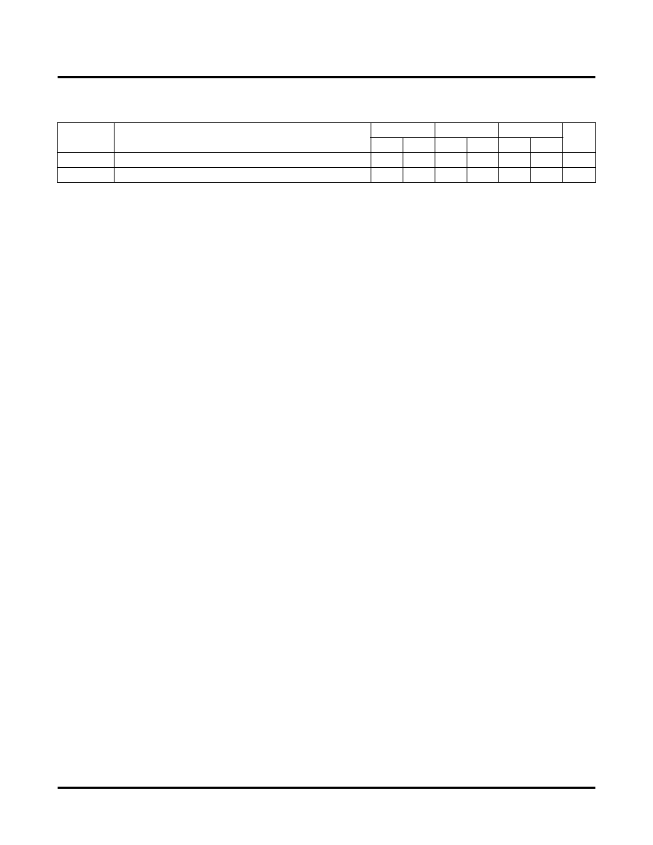
Lattice Semiconductor
ispMACH 4000V/B/C/Z Family Data Sheet
32
t
GPTOE
Global PT OE Delay
--
1.9
--
2.35
--
2.60
ns
t
PTOE
Macrocell PT OE Delay
--
2.4
--
3.35
--
2.60
ns
Note: Internal Timing Parameters are not tested and are for reference only. Refer to the timing model in this data sheet for
Timing v.2.2
further details.
ispMACH 4000Z Internal Timing Parameters (Cont.)
Over Recommended Operating Conditions
Parameter
Description
-35
-37
-42
Units
Min.
Max.
Min.
Max.
Min.
Max.

Lattice Semiconductor
ispMACH 4000V/B/C/Z Family Data Sheet
33
ispMACH 4000Z Internal Timing Parameters (Cont.)
Over Recommended Operating Conditions
Parameter
Description
-45
-5
-75
Units
Min.
Max.
Min.
Max.
Min.
Max.
In/Out Delays
t
IN
Input Buffer Delay
--
0.95
--
1.25
--
1.80
ns
t
GOE
Global OE Pin Delay
--
3.00
--
3.50
--
4.30
ns
t
GCLK_IN
Global Clock Input Buffer Delay
--
1.95
--
2.05
--
2.15
ns
t
BUF
Delay through Output Buffer
--
1.10
--
1.00
--
1.30
ns
t
EN
Output Enable Time
--
2.50
--
2.50
--
2.70
ns
t
DIS
Output Disable Time
--
2.50
--
2.50
--
2.70
ns
Routing/GLB Delays
t
ROUTE
Delay through GRP
--
2.25
--
2.05
--
2.50
ns
t
MCELL
Macrocell Delay
--
0.65
--
0.65
--
1.00
ns
t
INREG
Input Buffer to Macrocell Register Delay
--
1.00
--
1.00
--
1.00
ns
t
FBK
Internal Feedback Delay
--
0.35
--
0.05
--
0.05
ns
t
PDb
5-PT Bypass Propagation Delay
--
0.20
--
0.70
--
1.90
ns
t
PDi
Macrocell Propagation Delay
--
0.45
--
0.65
--
1.00
ns
Register/Latch Delays
t
S
D-Register Setup Time (Global Clock)
1.00
--
1.10
--
1.35
--
ns
t
S_PT
D-Register Setup Time (Product Term Clock)
2.10
--
1.90
--
2.45
--
ns
t
ST
T-Register Setup Time (Global Clock)
1.20
--
1.30
--
1.55
--
ns
t
ST_PT
T-register Setup Time (Product Term Clock)
2.30
--
2.10
--
2.75
--
ns
t
H
D-Register Hold Time
1.90
--
1.90
--
3.15
--
ns
t
HT
T-Resister Hold Time
1.90
--
1.90
--
3.15
--
ns
t
SIR
D-Input Register Setup Time (Global Clock)
1.30
--
1.10
--
0.75
--
ns
t
SIR_PT
D-Input Register Setup Time (Product Term Clock)
1.45
--
1.45
--
1.45
--
ns
t
HIR
D-Input Register Hold Time (Global Clock)
1.30
--
1.50
--
1.95
--
ns
t
HIR_PT
D-Input Register Hold Time (Product Term Clock)
1.00
--
1.00
--
1.18
--
ns
t
COi
Register Clock to Output/Feedback MUX Time
--
0.75
--
1.15
--
1.05
ns
t
CES
Clock Enable Setup Time
2.00
--
2.00
--
2.00
--
ns
t
CEH
Clock Enable Hold Time
0.00
--
0.00
--
0.00
--
ns
t
SL
Latch Setup Time (Global Clock)
1.00
--
1.00
--
1.65
--
ns
t
SL_PT
Latch Setup Time (Product Term Clock)
2.10
--
1.90
--
2.15
--
ns
t
HL
Latch Hold Time
2.00
--
2.00
--
1.17
--
ns
t
GOi
Latch Gate to Output/Feedback MUX Time
--
0.33
--
0.33
--
0.33
ns
t
PDLi
Propagation Delay through Transparent Latch to Output/
Feedback MUX
--
0.25
--
0.25
--
0.25
ns
t
SRi
Asynchronous Reset or Set to Output/Feedback MUX Delay
--
0.97
--
0.97
--
0.28
ns
t
SRR
Asynchronous Reset or Set Recovery Delay
--
1.80
--
1.80
--
1.67
ns
Control Delays
t
BCLK
GLB PT Clock Delay
--
1.55
--
1.55
--
1.25
ns
t
PTCLK
Macrocell PT Clock Delay
--
1.55
--
1.55
--
1.25
ns
t
BSR
GLB PT Set/Reset Delay
--
1.83
--
1.83
--
1.83
ns
t
PTSR
Macrocell PT Set/Reset Delay
--
1.83
--
1.83
--
2.72
ns
t
GPTOE
Global PT OE Delay
--
4.30
--
4.20
--
3.50
ns

Lattice Semiconductor
ispMACH 4000V/B/C/Z Family Data Sheet
34
t
PTOE
Macrocell PT OE Delay
--
2.50
--
2.70
--
2.00
ns
Note: Internal Timing Parameters are not tested and are for reference only. Refer to the timing model in this data sheet for
Timing v.2.2
further details.
ispMACH 4000Z Internal Timing Parameters (Cont.)
Over Recommended Operating Conditions
Parameter
Description
-45
-5
-75
Units
Min.
Max.
Min.
Max.
Min.
Max.

Lattice Semiconductor
ispMACH 4000V/B/C/Z Family Data Sheet
35
ispMACH 4000V/B/C Timing Adders
1
Adder
Type
Base
Parameter
Description
-25
-27
-3
-35
Units
Min.
Max.
Min.
Max.
Min.
Max.
Min.
Max.
Optional Delay Adders
t
INDIO
t
INREG
Input register delay
--
0.95
--
1.00
--
1.00
--
1.00
ns
t
EXP
t
MCELL
Product term expander
delay
--
0.33
--
0.33
--
0.33
--
0.33
ns
t
ORP
--
Output routing pool delay
--
0.05
--
0.05
--
0.05
--
0.05
ns
t
BLA
t
ROUTE
Additional block loading
adder
--
0.03
--
0.05
--
0.05
--
0.05
ns
t
IOI
Input Adjusters
LVTTL_in
t
IN
, t
GCLK_IN
,
t
GOE
Using LVTTL standard
--
0.60
--
0.60
--
0.60
--
0.60
ns
LVCMOS33_in
t
IN
, t
GCLK_IN
,
t
GOE
Using LVCMOS 3.3
standard
--
0.60
--
0.60
--
0.60
--
0.60
ns
LVCMOS25_in
t
IN
, t
GCLK_IN
,
t
GOE
Using LVCMOS 2.5
standard
--
0.60
--
0.60
--
0.60
--
0.60
ns
LVCMOS18_in
t
IN
, t
GCLK_IN
,
t
GOE
Using LVCMOS 1.8
standard
--
0.00
--
0.00
--
0.00
--
0.00
ns
PCI_in
t
IN
, t
GCLK_IN
,
t
GOE
Using PCI compatible
input
--
0.60
--
0.60
--
0.60
--
0.60
ns
t
IOO
Output Adjusters
LVTTL_out
t
BUF
, t
EN
, t
DIS
Output configured as
TTL buffer
--
0.20
--
0.20
--
0.20
--
0.20
ns
LVCMOS33_out t
BUF
, t
EN
, t
DIS
Output configured as
3.3V buffer
--
0.20
--
0.20
--
0.20
--
0.20
ns
LVCMOS25_out t
BUF
, t
EN
, t
DIS
Output configured as
2.5V buffer
--
0.10
--
0.10
--
0.10
--
0.10
ns
LVCMOS18_out t
BUF
, t
EN
, t
DIS
Output configured as
1.8V buffer
--
0.00
--
0.00
--
0.00
--
0.00
ns
PCI_out
t
BUF
, t
EN
, t
DIS
Output configured as
PCI compatible buffer
--
0.20
--
0.20
--
0.20
--
0.20
ns
Slow Slew
t
BUF
, t
EN
Output configured for
slow slew rate
--
1.00
--
1.00
--
1.00
--
1.00
ns
Note: Open drain timing is the same as corresponding LVCMOS timing.
Timing v.3.2
1. Refer to Technical Note TN1004: ispMACH 4000 Timing Model Design and Usage Guidelines for information regarding use of these adders.

Lattice Semiconductor
ispMACH 4000V/B/C/Z Family Data Sheet
36
ispMACH 4000V/B/C Timing Adders
1
(Cont.)
Adder
Type
Base
Parameter
Description
-5
-75
-10
Units
Min.
Max.
Min.
Max.
Min.
Max.
Optional Delay Adders
t
INDIO
t
INREG
Input register delay
--
1.00
--
1.00
--
1.00
ns
t
EXP
t
MCELL
Product term expander delay
--
0.33
--
0.33
--
0.33
ns
t
ORP
--
Output routing pool delay
--
0.05
--
0.05
--
0.05
ns
t
BLA
t
ROUTE
Additional block loading adder
--
0.05
--
0.05
--
0.05
ns
t
IOI
Input Adjusters
LVTTL_in
t
IN
, t
GCLK_IN
,
t
GOE
Using LVTTL standard
--
0.60
--
0.60
--
0.60
ns
LVCMOS33_in
t
IN
, t
GCLK_IN
,
t
GOE
Using LVCMOS 3.3 standard
--
0.60
--
0.60
--
0.60
ns
LVCMOS25_in
t
IN
, t
GCLK_IN
,
t
GOE
Using LVCMOS 2.5 standard
--
0.60
--
0.60
--
0.60
ns
LVCMOS18_in
t
IN
, t
GCLK_IN
,
t
GOE
Using LVCMOS 1.8 standard
--
0.00
--
0.00
--
0.00
ns
PCI_in
t
IN
, t
GCLK_IN
,
t
GOE
Using PCI compatible input
--
0.60
--
0.60
--
0.60
ns
t
IOO
Output Adjusters
LVTTL_out
t
BUF
, t
EN
, t
DIS
Output configured as TTL buffer
--
0.20
--
0.20
--
0.20
ns
LVCMOS33_out t
BUF
, t
EN
, t
DIS
Output configured as 3.3V buffer
--
0.20
--
0.20
--
0.20
ns
LVCMOS25_out t
BUF
, t
EN
, t
DIS
Output configured as 2.5V buffer
--
0.10
--
0.10
--
0.10
ns
LVCMOS18_out t
BUF
, t
EN
, t
DIS
Output configured as 1.8V buffer
--
0.00
--
0.00
--
0.00
ns
PCI_out
t
BUF
, t
EN
, t
DIS
Output configured as PCI compatible
buffer
--
0.20
--
0.20
--
0.20
ns
Slow Slew
t
BUF
, t
EN
Output configured for slow slew rate
--
1.00
--
1.00
--
1.00
ns
Note: Open drain timing is the same as corresponding LVCMOS timing.
Timing v.3.2
1. Refer to Technical Note TN1004: ispMACH 4000 Timing Model Design and Usage Guidelines for information regarding use of these adders.

Lattice Semiconductor
ispMACH 4000V/B/C/Z Family Data Sheet
37
ispMACH 4000Z Timing Adders
1
Adder
Type
Base
Parameter
Description
-35
-37
-42
Units
Min.
Max.
Min.
Max.
Min.
Max.
Optional Delay Adders
t
INDIO
t
INREG
Input register delay
--
1.00
--
1.00
--
1.30
ns
t
EXP
t
MCELL
Product term expander
delay
--
0.40
--
0.40
--
0.45
ns
t
ORP
--
Output routing pool
delay
--
0.40
--
0.40
--
0.40
ns
t
BLA
t
ROUTE
Additional block load-
ing adder
--
0.04
--
0.05
--
0.05
ns
t
IOI
Input Adjusters
LVTTL_in
t
IN,
t
GCLK_IN,
t
GOE
Using LVTTL standard
--
0.60
--
0.60
--
0.60
ns
LVCMOS33_in
t
IN,
t
GCLK_IN,
t
GOE
Using LVCMOS 3.3
standard
--
0.60
--
0.60
--
0.60
ns
LVCMOS25_in
t
IN,
t
GCLK_IN,
t
GOE
Using LVCMOS 2.5
standard
--
0.60
--
0.60
--
0.60
ns
LVCMOS18_in
t
IN,
t
GCLK_IN,
t
GOE
Using LVCMOS 1.8
standard
--
0.00
--
0.00
--
0.00
ns
PCI_in
t
IN,
t
GCLK_IN,
t
GOE
Using PCI compatible
input
--
0.60
--
0.60
--
0.60
ns
t
IOO
Output Adjusters
LVTTL_out
t
BUF,
t
EN,
t
DIS
Output configured as
TTL buffer
--
0.20
--
0.20
--
0.20
ns
LVCMOS33_out
t
BUF,
t
EN,
t
DIS
Output configured as
3.3V buffer
--
0.20
--
0.20
--
0.20
ns
LVCMOS25_out
t
BUF,
t
EN,
t
DIS
Output configured as
2.5V buffer
--
0.10
--
0.10
--
0.10
ns
LVCMOS18_out
t
BUF,
t
EN,
t
DIS
Output configured as
1.8V buffer
--
0.00
--
0.00
--
0.00
ns
PCI_out
t
BUF,
t
EN,
t
DIS
Output configured as
PCI compatible buffer
--
0.20
--
0.20
--
0.20
ns
Slow Slew
t
BUF,
t
EN
Output configured for
slow slew rate
--
1.00
--
1.00
--
1.00
ns
Note: Open drain timing is the same as corresponding LVCMOS timing.
Timing v.2.2
1. Refer to Technical Note TN 1004, ispMACH 4000 Timing Model Design and Usage Guidelines for information regarding the use of these
adders.
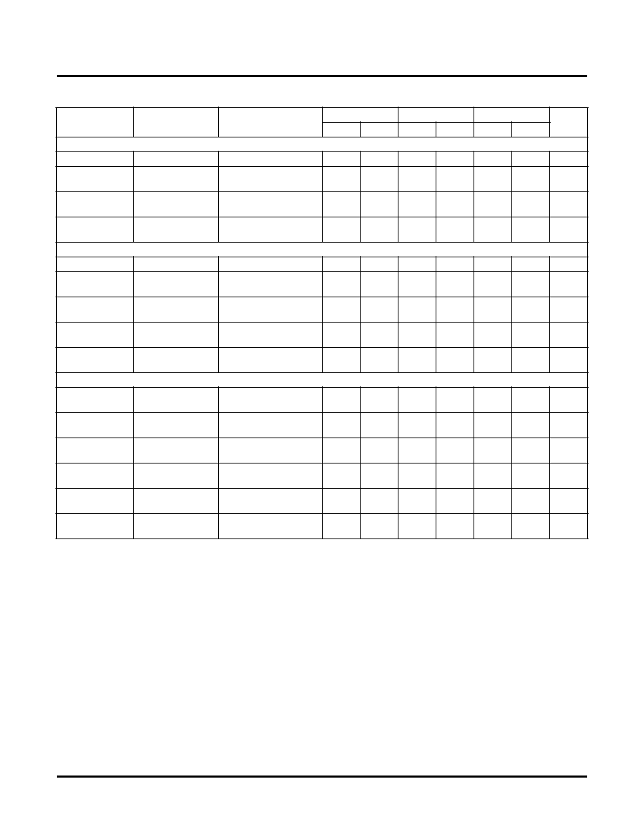
Lattice Semiconductor
ispMACH 4000V/B/C/Z Family Data Sheet
38
ispMACH 4000Z Timing Adders (Cont.)
1
Adder
Type
Base
Parameter
Description
-45
-5
-75
Units
Min.
Max.
Min.
Max.
Min.
Max.
Optional Delay Adders
t
INDIO
t
INREG
Input register delay
--
1.30
--
1.30
--
1.30
ns
t
EXP
t
MCELL
Product term expander
delay
--
0.45
--
0.45
--
0.50
ns
t
ORP
--
Output routing pool
delay
--
0.40
--
0.40
--
0.40
ns
t
BLA
t
ROUTE
Additional block load-
ing adder
--
0.05
--
0.05
--
0.05
ns
t
IOI
Input Adjusters
LVTTL_in
t
IN,
t
GCLK_IN,
t
GOE
Using LVTTL standard
--
0.60
--
0.60
--
0.60
ns
LVCMOS33_in
t
IN,
t
GCLK_IN,
t
GOE
Using LVCMOS 3.3
standard
--
0.60
--
0.60
--
0.60
ns
LVCMOS25_in
t
IN,
t
GCLK_IN,
t
GOE
Using LVCMOS 2.5
standard
--
0.60
--
0.60
--
0.60
ns
LVCMOS18_in
t
IN,
t
GCLK_IN,
t
GOE
Using LVCMOS 1.8
standard
--
0.00
--
0.00
--
0.00
ns
PCI_in
t
IN,
t
GCLK_IN,
t
GOE
Using PCI compatible
input
--
0.60
--
0.60
--
0.60
ns
t
IOO
Output Adjusters
LVTTL_out
t
BUF,
t
EN,
t
DIS
Output configured as
TTL buffer
--
0.20
--
0.20
--
0.20
ns
LVCMOS33_out t
BUF,
t
EN,
t
DIS
Output configured as
3.3V buffer
--
0.20
--
0.20
--
0.20
ns
LVCMOS25_out t
BUF,
t
EN,
t
DIS
Output configured as
2.5V buffer
--
0.10
--
0.10
--
0.10
ns
LVCMOS18_out t
BUF,
t
EN,
t
DIS
Output configured as
1.8V buffer
--
0.00
--
0.00
--
0.00
ns
PCI_out
t
BUF,
t
EN,
t
DIS
Output configured as
PCI compatible buffer
--
0.20
--
0.20
--
0.20
ns
Slow Slew
t
BUF,
t
EN
Output configured for
slow slew rate
--
1.00
--
1.00
--
1.00
ns
Note: Open drain timing is the same as corresponding LVCMOS timing.
Timing v.2.2
1. Refer to Technical Note TN 1004, ispMACH 4000 Timing Model Design and Usage Guidelines for information regarding use of these
adders.

Lattice Semiconductor
ispMACH 4000V/B/C/Z Family Data Sheet
39
Boundary Scan Waveforms and Timing Specifications
Symbol
Parameter
Min.
Max.
Units
t
BTCP
TCK [BSCAN test] clock cycle
40
--
ns
t
BTCH
TCK [BSCAN test] pulse width high
20
--
ns
t
BTCL
TCK [BSCAN test] pulse width low
20
--
ns
t
BTSU
TCK [BSCAN test] setup time
8
--
ns
t
BTH
TCK [BSCAN test] hold time
10
--
ns
t
BRF
TCK [BSCAN test] rise and fall time
50
--
mV/ns
t
BTCO
TAP controller falling edge of clock to valid output
--
10
ns
t
BTOZ
TAP controller falling edge of clock to data output disable
--
10
ns
t
BTVO
TAP controller falling edge of clock to data output enable
--
10
ns
t
BTCPSU
BSCAN test Capture register setup time
8
--
ns
t
BTCPH
BSCAN test Capture register hold time
10
--
ns
t
BTUCO
BSCAN test Update reg, falling edge of clock to valid output
--
25
ns
t
BTUOZ
BSCAN test Update reg, falling edge of clock to output disable
--
25
ns
t
BTUOV
BSCAN test Update reg, falling edge of clock to output enable
--
25
ns

Lattice Semiconductor
ispMACH 4000V/B/C/Z Family Data Sheet
40
Power Consumption
Power Estimation Coefficients
1
Device
A
B
ispMACH 4032V/B
11.3
0.010
ispMACH 4032C
1.3
0.010
ispMACH 4064V/B
11.5
0.010
ispMACH 4064C
1.5
0.010
ispMACH 4128V/B
11.5
0.011
ispMACH 4128C
1.5
0.011
ispMACH 4256V/B
12
0.011
ispMACH 4256C
2
0.011
ispMACH 4384V/B
12.5
0.013
ispMACH 4384C
2.5
0.013
ispMACH 4512V/B
13
0.013
ispMACH 4512C
3
0.013
ispMACH 4032ZC
0.010
0.010
ispMACH 4064ZC
0.011
0.010
ispMACH 4128ZC
0.012
0.010
ispMACH 4256ZC
0.013
0.010
1. For further information about the use of these coefficients, refer to Technical Note
TN1005, Power Estimation in ispMACH 4000V/B/C/Z Devices.
0
100
50
50
100
200
150
250
150
200
250
300
350
400
Frequency (MHz)
I
CC
(mA)
I
CC
(mA)
Note: The devices are configured with maximum number
of 16-bit counters, typical current at 1.8V, 25�C.
150
200
300
250
100
50
0
4032V/B
4064V/B
4128V/B
4384V/B
4256V/B
4512V/B
ispMACH 4000C
Typical I
CC
vs. Frequency
Note: The devices are configured with maximum number
of 16-bit counters, typical current at 3.3V, 2.5V, 25�C.
4032C
4064C
4128C
4384C
4256C
4512C
ispMACH 4000V/B
Typical I
CC
vs. Frequency
4032ZC
4064ZC
4128ZC
4256ZC
60
80
100
40
20
0
100
50
150
200
250
300
350
400
Frequency (MHz)
I
CC
(mA)
150
200
300
250
100
50
0
Note: The devices are configured with maximum number
of 16-bit counters, typical current at 1.8V, 25�C.
ispMACH 4000Z
Typical I
CC
vs. Frequency
(Preliminary Information)
0
300
Frequency (MHz)
0

Lattice Semiconductor
ispMACH 4000V/B/C/Z Family Data Sheet
41
Switching Test Conditions
Figure 12 shows the output test load that is used for AC testing. The specific values for resistance, capacitance,
voltage, and other test conditions are shown in Table 11.
Figure 12. Output Test Load, LVTTL and LVCMOS Standards
Table 11. Test Fixture Required Components
Test Condition
R
1
R
2
C
L
1
Timing Ref.
V
CCO
LVCMOS I/O, (L -> H, H -> L)
106 106
35pF
LVCMOS 3.3 = 1.5V
LVCMOS 3.3 = 3.0V
LVCMOS 2.5 = V
CCO
/2
LVCMOS 2.5 = 2.3V
LVCMOS 1.8 = V
CCO
/2
LVCMOS 1.8 = 1.65V
LVCMOS I/O (Z -> H)
106
35pF
1.5V
3.0V
LVCMOS I/O (Z -> L)
106
35pF
1.5V
3.0V
LVCMOS I/O (H -> Z)
106
5pF
V
OH
- 0.3
3.0V
LVCMOS I/O (L -> Z)
106
5pF
V
OL
+ 0.3
3.0V
1. C
L
includes test fixtures and probe capacitance.
V
CCO
R1
R2
CL
DUT
Test
Point
0213A/ispm4k

Lattice Semiconductor
ispMACH 4000V/B/C/Z Family Data Sheet
42
Signal Descriptions
ispMACH 4000V/B/C ORP Reference Table
ispMACH 4000Z ORP Reference Table
Signal Names
Description
TMS
Input � This pin is the IEEE 1149.1 Test Mode Select input, which is used to control
the state machine
TCK
Input � This pin is the IEEE 1149.1 Test Clock input pin, used to clock through the
state machine
TDI
Input � This pin is the IEEE 1149.1 Test Data In pin, used to load data
TDO
Output � This pin is the IEEE 1149.1 Test Data Out pin used to shift data out
GOE0/IO, GOE1/IO
These pins are configured to be either Global Output Enable Input or as general I/O
pins
GND
Ground
NC
Not Connected
V
CC
The power supply pins for logic core
CLK0/I, CLK1/I, CLK2/I, CLK3/I
These pins are configured to be either CLK input or as an input
V
CCO0
, V
CCO1
The power supply pins for each I/O bank
yzz
Input/Output
1
� These are the general purpose I/O used by the logic array. y is GLB
reference (alpha) and z is macrocell reference (numeric). z: 0-15
ispMACH 4032
y: A-B
ispMACH 4064
y: A-D
ispMACH 4128
y: A-H
ispMACH 4256
y: A-P
ispMACH 4384
y: A-P, AX-HX
ispMACH 4512
y: A-P, AX-PX
1. In some packages, certain I/Os are only available for use as inputs. See the signal connections table for details.
4032V/B/C
4064V/B/C
4128V/B/C
4256V/B/C
4384V/B/C
4512V/B/C
Number of I/Os
30
1
32
30
2
32
64
64
92
3
96
64
96
4
128
160
128
192
128
208
Number of GLBs
2
2
4
4
4
8
8
8
16
16
16
16
16
16
16
16
Number of I/Os /
GLB
16
16
8
8
16
8
12
12
4
8
8
10
8
8
8
Mixture
of 8 & 4
5
Reference ORP
Table
16 I/Os /
GLB
8 I/Os /
GLB
16 I/Os /
GLB
8 I/Os /
GLB
12 I/Os /
GLB
4 I/Os /
GLB
8 I/Os /
GLB
8 I/Os /
GLB
10 I/Os /
GLB
8 I/Os /
GLB
8 I/Os /
GLB
8 I/Os /
GLB
4 I/Os /
GLB
1. 32-macrocell device, 44 TQFP: 2 GLBs have 15 out of 16 I/Os bonded out.
2. 64-macrocesll device, 44 TQFP: 2 GLBs have 7 out of 8 I/Os bonded out.
3. 128-macrocell device, 128 TQFP: 4 GLBs have 11 out of 12 I/Os
4. 256-macrocell device, 144 TQFP: 16 GLBs have 6 I/Os per
5. 512-macrocell device: 20 GLBs have 8 I/Os per, 12 GLBs have 4 I/Os per
4032Z
4064Z
4128Z
4256Z
Number of I/Os
32
32
64
64
96
64
96
1
128
Number of GLBs
2
4
4
8
8
16
16
16
Number of I/Os / GLB
16
8
16
8
12
4
8
8
Reference ORP Table
16 I/Os /
GLB
8 I/Os /
GLB
16 I/Os /
GLB
8 I/Os /
GLB
12 I/Os /
GLB
4 I/Os /
GLB
8 I/Os /
GLB
8 I/Os /
GLB
1. 256-macrocell device, 132 csBGA: 16 GLBs have 6 I/Os per

Lattice Semiconductor
ispMACH 4000V/B/C/Z Family Data Sheet
43
ispMACH 4000V/B/C/Z Power Supply and NC Connections
1
Signal
44-pin TQFP
2
48-pin TQFP
2
56-ball csBGA
3
100-pin TQFP
2
128-pin TQFP
2
VCC
11, 33
12, 36
K2, A9
25, 40, 75, 90
32, 51, 96, 115
VCCO0
VCCO (Bank 0)
6
6
F3
13, 33, 95
3, 17, 30, 41, 122
VCCO1
VCCO (Bank 0)
28
30
E8
45, 63, 83
58, 67, 81, 94, 105
GND
12, 34
13, 37
H3, C8
1, 26, 51, 76
1, 33, 65, 97
GND (Bank 0)
5
5
D3
7, 18, 32, 96
10, 24, 40, 113, 123
GND (Bank 1)
27
29
G8
46, 57, 68, 82
49, 59, 74, 88, 104
NC
--
--
4032Z: A8, B10, E1,
E3, F8, F10, J1, K3
--
--
1. All grounds must be electrically connected at the board level. However, for the purposes of I/O current loading, grounds are associated with
the bank shown.
2. Pin orientation follows the conventional order from pin 1 marking of the top side view and counter-clockwise.
3. Pin orientation A1 starts from the upper left corner of the top side view with alphabetical order ascending vertically and numerical order
ascending horizontally.

Lattice Semiconductor
ispMACH 4000V/B/C/Z Family Data Sheet
44
ispMACH 4000V/B/C/Z Power Supply and NC Connections
1
(Cont.)
Signal
132-ball csBGA
7
144-pin TQFP
4
176-pin TQFP
4
256-ball fpBGA
2, 3, 7
VCC
P1, A14, B7, N8
36, 57, 108, 129
42, 69, 88, 130,
157, 176
B2, B15, G8, G9, K8, K9, R2, R15
VCCO0
VCCO (Bank 0)
G3, P5, C1
8
, M2
8
,
C5
3, 19, 34, 47, 136
4, 22, 40, 56, 166
D6, F4, H7, J7, L4, N6
VCCO1
VCCO (Bank 1)
M10, M14
8
, H12,
A10, C13
8
64, 75, 91, 106, 119 78, 92, 110, 128,
144
D11, F13, H10, J10, L13, N11
GND
B1, P2, N14, A13
1, 37, 73, 109
2, 46
5
, 65, 90, 134,
153
A1, A16, C6, C11, F3, F14, G7, G10, H8,
H9, J8, J9, K7, K10, L3, L14, P6, P11, T1,
T16
GND (Bank 0)
E2, K2, N4, B4
10, 18
6
, 27, 46, 127,
137
13, 31, 55, 155,
167
GND (Bank 1)
N11, K13, E13, B11 55, 65, 82, 90
6
, 99,
118
67, 79, 101, 119,
143
NC
4064Z: C1, C3, E1,
E3, H2, J3, K1, M2,
M4, N5, P7, P8, M8,
P10, P11, P14, M12,
K14, K12, G13,
G14, E14, C13, B13,
B10, C10, A7, B5,
A5, A4, A1
4128Z: P8, A7
4128V: 17, 20, 38,
45, 72, 89, 92, 110,
117, 144
4256V: 18, 90
1, 43, 44, 45, 89,
131, 132, 133
4256V/B/C, 128 I/O: A4, A5, A6, A11, A12,
A13, A15, B5, B6, B11, B12, B14, C7, D1,
D4, D5, D10, D12, D16, E1, E2, E4, E5, E7,
E10, E13, E14, E15, E16, F1, F2, F15, F16,
G1, G4, G5, G6, G12, G13, G14, J11, K3,
K4, K15, L1, L2, L12, L15, L16, M1, M2, M3,
M4, M5, M12, M13, M15, M16, N1, N2, N7,
N10, N12, N14, P5, P12, R4, R5, R6, R11,
R12, R16, T2, T4, T5, T6, T11, T12, T13, T15
4256V/B/C, 160 I/O: A5, A12, A15, B5, B6,
B11, B12, B14, D4, D5, D12, E1, E4, E5,
E13, E15, E16, F1, F2, F15, G1, G5, G12,
G14, L1, L2, L12, L15, L16, M1, M2, M3,
M12, M16, N1, N12, N14, P5, R4, R5, R6,
R11, R12, R16, T4, T5, T12, T15
4384V/B/C: B5, B12, D5, D12, E1, E15,
E16, F2, L12, M1, M2, M16, N12, R5, R12,
T4
4512V/B/C: None
1. All grounds must be electrically connected at the board level. However, for the purposes of I/O current loading, grounds are associated with
the bank shown.
2. Internal GNDs and I/O GNDs (Bank 0/1) are connected inside package.
3. V
CCO
balls connect to two power planes within the package, one for V
CCO0
and one for V
CCO1
.
4. Pin orientation follows the conventional order from pin 1 marking of the top side view and counter-clockwise.
5. ispMACH 4384V/B/C pin 46 is tied to GND (Bank 0).
6. ispMACH 4128V only.
7. Pin orientation A1 starts from the upper left corner of the top side view with alphabetical order ascending vertically and numerical order
ascending horizontally.
8. ispMACH 4128Z and 4256Z only. NC for ispMACH 4064Z.

Lattice Semiconductor
ispMACH 4000V/B/C/Z Family Data Sheet
45
ispMACH 4032V/B/C and 4064V/B/C Logic Signal Connections:
44-Pin TQFP
Pin Number
Bank Number
ispMACH 4032V/B/C
ispMACH 4064V/B/C
GLB/MC/Pad
ORP
GLB/MC/Pad
ORP
1
-
TDI
-
TDI
-
2
0
A5
A^5
A10
A^5
3
0
A6
A^6
A12
A^6
4
0
A7
A^7
A14
A^7
5
0
GND (Bank 0)
-
GND (Bank 0)
-
6
0
VCCO (Bank 0)
-
VCCO (Bank 0)
-
7
0
A8
A^8
B0
B^0
8
0
A9
A^9
B2
B^1
9
0
A10
A^10
B4
B^2
10
-
TCK
-
TCK
-
11
-
VCC
-
VCC
-
12
-
GND
-
GND
-
13
0
A12
A^12
B8
B^4
14
0
A13
A^13
B10
B^5
15
0
A14
A^14
B12
B^6
16
0
A15
A^15
B14
B^7
17
1
CLK2/I
-
CLK2/I
-
18
1
B0 B^0
C0
C^0
19
1
B1
B^1
C2
C^1
20
1
B2
B^2
C4
C^2
21
1
B3
B^3
C6
C^3
22
1
B4
B^4
C8
C^4
23
-
TMS
-
TMS
-
24
1
B5
B^5
C10
C^5
25
1
B6
B^6
C12
C^6
26
1
B7
B^7
C14
C^7
27
1
GND (Bank 1)
-
GND (Bank 1)
-
28
1
VCCO (Bank 1)
-
VCCO (Bank 1)
-
29
1
B8
B^8
D0
D^0
30
1
B9
B^9
D2
D^1
31
1
B10
B^10
D4
D^2
32
-
TDO
-
TDO
-
33
-
VCC
-
VCC
-
34
-
GND
-
GND
-
35
1
B12
B^12
D8
D^4
36
1
B13
B^13
D10
D^5
37
1
B14
B^14
D12
D^6
38
1
B15/GOE1
B^15
D14/GOE1
D^7
39
0
CLK0/I
-
CLK0/I
-
40
0
A0/GOE0
A^0
A0/GOE0
A^0
41
0
A1
A^1
A2
A^1

Lattice Semiconductor
ispMACH 4000V/B/C/Z Family Data Sheet
46
42
0
A2
A^2
A4
A^2
43
0
A3
A^3
A6
A^3
44
0
A4
A^4
A8
A^4
ispMACH 4032V/B/C/Z and 4064V/B/C/Z Logic Signal Connections:
48-Pin TQFP
Pin
Number
Bank
Number
ispMACH 4032V/B/C
ispMACH 4064V/B/C
ispMACH 4064Z
GLB/MC/Pad
ORP
GLB/MC/Pad
ORP
GLB/MC/Pad
ORP
1
-
TDI
-
TDI
-
TDI
-
2
0
A5
A^5
A10
A^5
A8
A^5
3
0
A6
A^6
A12
A^6
A10
A^6
4
0
A7
A^7
A14
A^7
A11
A^7
5
0
GND (Bank 0)
-
GND (Bank 0)
-
GND (Bank 0)
-
6
0
VCCO (Bank 0)
-
VCCO (Bank 0)
-
VCCO (Bank 0)
-
7
0
A8
A^8
B0
B^0
B15
B^7
8
0
A9
A^9
B2
B^1
B12
B^6
9
0
A10
A^10
B4
B^2
B10
B^5
10
0
A11
A^11
B6
B^3
B8
B^4
11
-
TCK
-
TCK
-
TCK
-
12
-
VCC
-
VCC
-
VCC
-
13
-
GND
-
GND
-
GND
-
14
0
A12
A^12
B8
B^4
B6
B^3
15
0
A13
A^13
B10
B^5
B4
B^2
16
0
A14
A^14
B12
B^6
B2
B^1
17
0
A15
A^15
B14
B^7
B0
B^0
18
0
CLK1/I
-
CLK1/I
-
CLK1/I
-
19
1
CLK2/I
-
CLK2/I
-
CLK2/I
-
20
1
B0
B^0
C0
C^0
C0
C^0
21
1
B1
B^1
C2
C^1
C1
C^1
22
1
B2
B^2
C4
C^2
C2
C^2
23
1
B3
B^3
C6
C^3
C4
C^3
24
1
B4
B^4
C8
C^4
C6
C^4
25
-
TMS
-
TMS
-
TMS
-
26
1
B5
B^5
C10
C^5
C8
C^5
27
1
B6
B^6
C12
C^6
C10
C^6
28
1
B7
B^7
C14
C^7
C11
C^7
29
1
GND (Bank 1)
-
GND (Bank 1)
-
GND (Bank 1)
-
30
1
VCCO (Bank 1)
-
VCCO (Bank 1)
-
VCCO (Bank 1)
-
31
1
B8
B^8
D0
D^0
D15
D^7
32
1
B9
B^9
D2
D^1
D12
D^6
ispMACH 4032V/B/C and 4064V/B/C Logic Signal Connections:
44-Pin TQFP (Cont.)
Pin Number
Bank Number
ispMACH 4032V/B/C
ispMACH 4064V/B/C
GLB/MC/Pad
ORP
GLB/MC/Pad
ORP

Lattice Semiconductor
ispMACH 4000V/B/C/Z Family Data Sheet
47
33
1
B10
B^10
D4
D^2
D10
D^5
34
1
B11
B^11
D6
D^3
D8
D^4
35
-
TDO
-
TDO
-
TDO
-
36
-
VCC
-
VCC
-
VCC
-
37
-
GND
-
GND
-
GND
-
38
1
B12
B^12
D8
D^4
D6
D^3
39
1
B13
B^13
D10
D^5
D4
D^2
40
1
B14
B^14
D12
D^6
D2
D^1
41
1
B15/GOE1
B^15
D14/GOE1
D^7
D0/GOE1
D^0
42
1
CLK3/I
-
CLK3/I
-
CLK3/I
-
43
0
CLK0/I
-
CLK0/I
-
CLK0/I
-
44
0
A0/GOE0
A^0
A0/GOE0
A^0
A0/GOE0
A^0
45
0
A1
A^1
A2
A^1
A1
A^1
46
0
A2
A^2
A4
A^2
A2
A^2
47
0
A3
A^3
A6
A^3
A4
A^3
48
0
A4
A^4
A8
A^4
A6
A^4
ispMACH 4032Z and 4064Z Logic Signal Connections: 56-Ball csBGA
Ball Number
Bank Number
ispMACH 4032Z
ispMACH 4064Z
GLB/MC/Pad
ORP
GLB/MC/Pad
ORP
B1
-
TDI
-
TDI
-
C3
0
A5
A^5
A8
A^5
C1
0
A6
A^6
A10
A^6
D1
0
A7
A^7
A11
A^7
D3
0
GND (Bank 0)
-
GND (Bank 0)
-
E3
0
NC
-
I
-
E1
0
NC
-
I
-
F3
0
VCCO (Bank 0)
-
VCCO (Bank 0)
-
F1
0
A8
A^8
B15
B^7
G3
0
A9
A^9
B12
B^6
G1
0
A10
A^10
B10
B^5
H1
0
A11
A^11
B8
B^4
J1
0
NC
-
I
-
K1
-
TCK
-
TCK
-
K2
-
VCC
-
VCC
-
H3
-
GND
-
GND
-
K3
-
I
-
K4
0
A12
A^12
B6
B^3
H4
0
A13
A^13
B4
B^2
H5
0
A14
A^14
B2
B^1
ispMACH 4032V/B/C/Z and 4064V/B/C/Z Logic Signal Connections:
48-Pin TQFP (Cont.)
Pin
Number
Bank
Number
ispMACH 4032V/B/C
ispMACH 4064V/B/C
ispMACH 4064Z
GLB/MC/Pad
ORP
GLB/MC/Pad
ORP
GLB/MC/Pad
ORP

Lattice Semiconductor
ispMACH 4000V/B/C/Z Family Data Sheet
48
K5
0
A15
A^15
B0
B^0
H6
0
CLK1/I
-
CLK1/I
-
K6
1
CLK2/I
-
CLK2/I
-
H7
1
B0
B^0
C0
C^0
K7
1
B1
B^1
C1
C^1
K8
1
B2
B^2
C2
C^2
K9
1
B3
B^3
C4
C^3
K10
1
B4
B^4
C6
C^4
J10
-
TMS
-
TMS
-
H8
1
B5
B^5
C8
C^5
H10
1
B6
B^6
C10
C^6
G10
1
B7
B^7
C11
C^7
G8
1
GND (Bank 1)
-
GND (Bank 1)
-
F8
1
NC
-
I
-
F10
1
NC
-
I
-
E8
1
VCCO (Bank 1)
-
VCCO (Bank 1)
-
E10
1
B8
B^8
D15
D^7
D8
1
B9
B^9
D12
D^6
D10
1
B10
B^10
D10
D^5
C10
1
B11
B^11
D8
D^4
B10
1
NC
-
I
-
A10
-
TDO
-
TDO
-
A9
-
VCC
-
VCC
-
C8
-
GND
-
GND
-
A8
1
NC
-
I
-
A7
1
B12
B^12
D6
D^3
C7
1
B13
B^13
D4
D^2
C6
1
B14
B^14
D2
D^1
A6
1
B15/GOE1
B^15
D0/GOE1
D^0
C5
1
CLK3/I
-
CLK3/I
-
A5
0
CLK0/I
-
CLK0/I
-
C4
0
A0/GOE0
A^0
A0/GOE0
A^0
A4
0
A1
A^1
A1
A^1
A3
0
A2
A^2
A2
A^2
A2
0
A3
A^3
A4
A^3
A1
0
A4
A^4
A6
A^4
ispMACH 4032Z and 4064Z Logic Signal Connections: 56-Ball csBGA (Cont.)
Ball Number
Bank Number
ispMACH 4032Z
ispMACH 4064Z
GLB/MC/Pad
ORP
GLB/MC/Pad
ORP

Lattice Semiconductor
ispMACH 4000V/B/C/Z Family Data Sheet
49
ispMACH 4064V/B/C/Z, 4128V/B/C/Z, 4256V/B/C/Z Logic Signal Connections:
100-Pin TQFP
Pin Number
Bank
Number
ispMACH 4064V/B/C/Z
ispMACH 4128V/B/C/Z
ispMACH 4256V/B/C/Z
GLB/MC/Pad
ORP
GLB/MC/Pad
ORP
GLB/MC/Pad
ORP
1
-
GND
-
GND
-
GND
-
2
-
TDI
-
TDI
-
TDI
-
3
0
A8
A^8
B0
B^0
C12
C^3
4
0
A9
A^9
B2
B^1
C10
C^2
5
0
A10
A^10
B4
B^2
C6
C^1
6
0
A11
A^11
B6
B^3
C2
C^0
7
0
GND (Bank 0)
-
GND (Bank 0)
-
GND (Bank 0)
-
8
0
A12
A^12
B8
B^4
D12
D^3
9
0
A13
A^13
B10
B^5
D10
D^2
10
0
A14
A^14
B12
B^6
D6
D^1
11
0
A15
A^15
B13
B^7
D4
D^0
12*
0
I
-
I -
I
-
13
0
VCCO (Bank 0)
-
VCCO (Bank 0)
-
VCCO (Bank 0)
-
14
0
B15
B^15
C14
C^7
E4
E^0
15
0
B14
B^14
C12
C^6
E6
E^1
16
0
B13
B^13
C10
C^5
E10
E^2
17
0
B12
B^12
C8
C^4
E12
E^3
18
0
GND (Bank 0)
-
GND (Bank 0)
-
GND (Bank 0)
-
19
0
B11
B^11
C6
C^3
F2
F^0
20
0
B10
B^10
C5
C^2
F6
F^1
21
0
B9
B^9
C4
C^1
F10
F^2
22
0
B8
B^8
C2
C^0
F12
F^3
23*
0
I
-
I
-
I
-
24
-
TCK
-
TCK
-
TCK
-
25
-
VCC
-
VCC
-
VCC
-
26
-
GND
-
GND
-
GND
-
27*
0
I
-
I
-
I
-
28
0
B7
B^7
D13
D^7
G12
G^3
29
0
B6
B^6
D12
D^6
G10
G^2
30
0
B5
B^5
D10
D^5
G6
G^1
31
0
B4
B^4
D8
D^4
G2
G^0
32
0
GND (Bank 0)
-
GND (Bank 0)
-
GND (Bank 0)
-
33
0
VCCO (Bank 0)
-
VCCO (Bank 0)
-
VCCO (Bank 0)
-
34
0
B3
B^3
D6
D^3
H12
H^3
35
0
B2
B^2
D4
D^2
H10
H^2
36
0
B1
B^1
D2
D^1
H6
H^1
37
0
B0
B^0
D0
D^0
H2
H^0
38
0
CLK1/I
-
CLK1/I
-
CLK1/I
-
39
1
CLK2/I
-
CLK2/I
-
CLK2/I
-
40
-
VCC
-
VCC
-
VCC
-
41
1
C0
C^0
E0
E^0
I2
I^0

Lattice Semiconductor
ispMACH 4000V/B/C/Z Family Data Sheet
50
42
1
C1
C^1
E2
E^1
I6
I^1
43
1
C2
C^2
E4
E^2
I10
I^2
44
1
C3
C^3
E6
E^3
I12
I^3
45
1
VCCO (Bank 1)
-
VCCO (Bank 1)
-
VCCO (Bank 1)
-
46
1
GND (Bank 1)
-
GND (Bank 1)
-
GND (Bank 1)
-
47
1
C4
C^4
E8
E^4
J2
J^0
48
1
C5
C^5
E10
E^5
J6
J^1
49
1
C6
C^6
E12
E^6
J10
J^2
50
1
C7
C^7
E14
E^7
J12
J^3
51
-
GND
-
GND
-
GND
-
52
-
TMS
-
TMS
-
TMS
-
53
1
C8
C^8
F0
F^0
K12
K^3
54
1
C9
C^9
F2
F^1
K10
K^2
55
1
C10
C^10
F4
F^2
K6
K^1
56
1
C11
C^11
F6
F^3
K2
K^0
57
1
GND (Bank 1)
-
GND (Bank 1)
-
GND (Bank 1)
-
58
1
C12
C^12
F8
F^4
L12
L^3
59
1
C13
C^13
F10
F^5
L10
L^2
60
1
C14
C^14
F12
F^6
L6
L^1
61
1
C15
C^15
F13
F^7
L4
L^0
62*
1
I
-
I
-
I
-
63
1
VCCO (Bank 1)
-
VCCO (Bank 1)
-
VCCO (Bank 1)
-
64
1
D15
D^15
G14
G^7
M4
M^0
65
1
D14
D^14
G12
G^6
M6
M^1
66
1
D13
D^13
G10
G^5
M10
M^2
67
1
D12
D^12
G8
G^4
M12
M^3
68
1
GND (Bank 1)
-
GND (Bank 1)
-
GND (Bank 1)
-
69
1
D11
D^11
G6
G^3
N2
N^0
70
1
D10
D^10
G5
G^2
N6
N^1
71
1
D9
D^9
G4
G^1
N10
N^2
72
1
D8
D^8
G2
G^0
N12
N^3
73*
1
I
-
I
-
I
-
74
-
TDO
-
TDO
-
TDO
-
75
-
VCC
-
VCC
-
VCC
-
76
-
GND
-
GND
-
GND
-
77*
1
I
-
I
-
I
-
78
1
D7
D^7
H13
H^7
O12
O^3
79
1
D6
D^6
H12
H^6
O10
O^2
80
1
D5
D^5
H10
H^5
O6
O^1
81
1
D4
D^4
H8
H^4
O2
O^0
82
1
GND (Bank 1)
-
GND (Bank 1)
-
GND (Bank 1)
-
ispMACH 4064V/B/C/Z, 4128V/B/C/Z, 4256V/B/C/Z Logic Signal Connections:
100-Pin TQFP (Cont.)
Pin Number
Bank
Number
ispMACH 4064V/B/C/Z
ispMACH 4128V/B/C/Z
ispMACH 4256V/B/C/Z
GLB/MC/Pad
ORP
GLB/MC/Pad
ORP
GLB/MC/Pad
ORP

Lattice Semiconductor
ispMACH 4000V/B/C/Z Family Data Sheet
51
83
1
VCCO (Bank 1)
-
VCCO (Bank 1)
-
VCCO (Bank 1)
-
84
1
D3
D^3
H6
H^3
P12
P^3
85
1
D2
D^2
H4
H^2
P10
P^2
86
1
D1
D^1
H2
H^1
P6
P^1
87
1
D0/GOE1
D^0
H0/GOE1
H^0
P2/OE1
P^0
88
1
CLK3/I
-
CLK3/I
-
CLK3/I
-
89
0
CLK0/I
-
CLK0/I
-
CLK0/I
-
90
-
VCC
-
VCC
-
VCC
-
91
0
A0/GOE0
A^0
A0/GOE0
A^0
A2/GOE0
A^0
92
0
A1
A^1
A2
A^1
A6
A^1
93
0
A2
A^2
A4
A^2
A10
A^2
94
0
A3
A^3
A6
A^3
A12
A^3
95
0
VCCO (Bank 0)
-
VCCO (Bank 0)
-
VCCO (Bank 0)
-
96
0
GND (Bank 0)
-
GND (Bank 0)
-
GND (Bank 0)
-
97
0
A4
A^4
A8
A^4
B2
B^0
98
0
A5
A^5
A10
A^5
B6
B^1
99
0
A6
A^6
A12
A^6
B10
B^2
100
0
A7
A^7
A14
A^7
B12
B^3
*This pin is input only.
ispMACH 4128V/B/C Logic Signal Connections: 128-Pin TQFP
Pin Number
Bank Number
ispMACH 4128V/B/C
GLB/MC/Pad
ORP
1
0
GND
-
2
0
TDI
-
3
0
VCCO (Bank 0)
-
4
0
B0
B^0
5
0
B1
B^1
6
0
B2
B^2
7
0
B4
B^3
8
0
B5
B^4
9
0
B6
B^5
10
0
GND (Bank 0)
-
11
0
B8
B^6
12
0
B9
B^7
13
0
B10
B^8
14
0
B12
B^9
15
0
B13
B^10
16
0
B14
B^11
17
0
VCCO (Bank 0)
-
18
0
C14
C^11
ispMACH 4064V/B/C/Z, 4128V/B/C/Z, 4256V/B/C/Z Logic Signal Connections:
100-Pin TQFP (Cont.)
Pin Number
Bank
Number
ispMACH 4064V/B/C/Z
ispMACH 4128V/B/C/Z
ispMACH 4256V/B/C/Z
GLB/MC/Pad
ORP
GLB/MC/Pad
ORP
GLB/MC/Pad
ORP

Lattice Semiconductor
ispMACH 4000V/B/C/Z Family Data Sheet
52
19
0
C13
C^10
20
0
C12
C^9
21
0
C10
C^8
22
0
C9
C^7
23
0
C8
C^6
24
0
GND (Bank 0)
-
25
0
C6
C^5
26
0
C5
C^4
27
0
C4
C^3
28
0
C2
C^2
29
0
C0
C^0
30
0
VCCO (Bank 0)
-
31
0
TCK
-
32
0
VCC
-
33
0
GND
-
34
0
D14
D^11
35
0
D13
D^10
36
0
D12
D^9
37
0
D10
D^8
38
0
D9
D^7
39
0
D8
D^6
40
0
GND (Bank 0)
-
41
0
VCCO (Bank 0)
-
42
0
D6
D^5
43
0
D5
D^4
44
0
D4
D^3
45
0
D2
D^2
46
0
D1
D^1
47
0
D0
D^0
48
0
CLK1/I
-
49
1
GND (Bank 1)
-
50
1
CLK2/I
-
51
1
VCC
-
52
1
E0
E^0
53
1
E1
E^1
54
1
E2
E^2
55
1
E4
E^3
56
1
E5
E^4
57
1
E6
E^5
58
1
VCCO (Bank 1)
-
59
1
GND (Bank 1)
-
60
1
E8
E^6
61
1
E9
E^7
ispMACH 4128V/B/C Logic Signal Connections: 128-Pin TQFP (Cont.)
Pin Number
Bank Number
ispMACH 4128V/B/C
GLB/MC/Pad
ORP

Lattice Semiconductor
ispMACH 4000V/B/C/Z Family Data Sheet
53
62
1
E10
E^8
63
1
E12
E^9
64
1
E14
E^11
65
1
GND
-
66
1
TMS
-
67
1
VCCO (Bank 1)
-
68
1
F0
F^0
69
1
F1
F^1
70
1
F2
F^2
71
1
F4
F^3
72
1
F5
F^4
73
1
F6
F^5
74
1
GND (Bank 1)
-
75
1
F8
F^6
76
1
F9
F^7
77
1
F10
F^8
78
1
F12
F^9
79
1
F13
F^10
80
1
F14
F^11
81
1
VCCO (Bank 1)
-
82
1
G14
G^11
83
1
G13
G^10
84
1
G12
G^9
85
1
G10
G^8
86
1
G9
G^7
87
1
G8
G^6
88
1
GND (Bank 1)
-
89
1
G6
G^5
90
1
G5
G^4
91
1
G4
G^3
92
1
G2
G^2
93
1
G0
G^0
94
1
VCCO (Bank 1)
-
95
1
TDO
-
96
1
VCC
-
97
1
GND
-
98
1
H14
H^11
99
1
H13
H^10
100
1
H12
H^9
101
1
H10
H^8
102
1
H9
H^7
103
1
H8
H^6
104
1
GND (Bank 1)
-
ispMACH 4128V/B/C Logic Signal Connections: 128-Pin TQFP (Cont.)
Pin Number
Bank Number
ispMACH 4128V/B/C
GLB/MC/Pad
ORP

Lattice Semiconductor
ispMACH 4000V/B/C/Z Family Data Sheet
54
105
1
VCCO (Bank 1)
-
106
1
H6
H^5
107
1
H5
H^4
108
1
H4
H^3
109
1
H2
H^2
110
1
H1
H^1
111
1
H0/GOE1
H^0
112
1
CLK3/I
-
113
0
GND (Bank 0)
-
114
0
CLK0/I
-
115
0
VCC
-
116
0
A0/GOE0
A^0
117
0
A1
A^1
118
0
A2
A^2
119
0
A4
A^3
120
0
A5
A^4
121
0
A6
A^5
122
0
VCCO (Bank 0)
-
123
0
GND (Bank 0)
-
124
0
A8
A^6
125
0
A9
A^7
126
0
A10
A^8
127
0
A12
A^9
128
0
A14
A^11
ispMACH 4064Z, 4128Z and 4256Z Logic Signal Connections:
132-Ball csBGA
Ball Number Bank Number
ispMACH 4064Z
ispMACH 4128Z
ispMACH 4256Z
GLB/MC/Pad
ORP
GLB/MC/Pad
ORP
GLB/MC/Pad
ORP
B1
-
GND
-
GND
-
GND
-
B2
-
TDI
-
TDI
-
TDI
-
C1
0
NC
-
VCCO (Bank 0)
-
VCCO (Bank 0)
-
C3
0
NC
-
B0
B^0
C12
C^6
C2
0
A8
A^8
B1
B^1
C10
C^5
D1
0
A9
A^9
B2
B^2
C8
C^4
D3
0
A10
A^10
B4
B^3
C6
C^3
D2
0
A11
A^11
B5
B^4
C4
C^2
E1
0
NC
B6
B^5
C2
C^1
E2
0
GND (Bank 0)
-
GND (Bank 0)
-
GND (Bank 0)
-
E3
0
NC
-
B8
B^6
D12
D^6
F2
0
A12
A^12
B9
B^7
D10
D^5
ispMACH 4128V/B/C Logic Signal Connections: 128-Pin TQFP (Cont.)
Pin Number
Bank Number
ispMACH 4128V/B/C
GLB/MC/Pad
ORP

Lattice Semiconductor
ispMACH 4000V/B/C/Z Family Data Sheet
55
F1
0
A13
A^13
B10
B^8
D8
D^4
F3
0
A14
A^14
B12
B^9
D6
D^3
G1
0
A15
A^15
B13
B^10
D4
D^2
G2
0
I
-
B14
B^11
D2
D^1
G3
0
VCCO (Bank 0)
-
VCCO (Bank 0)
-
VCCO (Bank 0)
-
H2
0
NC
-
C14
C^11
E2
E^1
H1
0
B15
B^15
C13
C^10
E4
E^2
H3
0
B14
B^14
C12
C^9
E6
E^3
J1
0
B13
B^13
C10
C^8
E8
E^4
J2
0
B12
B^12
C9
C^7
E10
E^5
J3
0
NC
-
C8
C^6
E12
E^6
K2
0
GND (Bank 0)
-
GND (Bank 0)
-
GND (Bank 0)
-
K1
0
NC
-
C6
C^5
F2
F^1
K3
0
B11
B^11
C5
C^4
F4
F^2
L2
0
B10
B^10
C4
C^3
F6
F^3
L1
0
B9
B^9
C2
C^2
F8
F^4
L3
0
B8
B^8
C1
C^1
F10
F^5
M1
0
I
-
C0
C^0
F12
F^6
M2
0
NC
-
VCCO (Bank 0)
-
VCCO (Bank 0)
-
N1
-
TCK
-
TCK
-
TCK
-
P1
-
VCC
-
VCC
-
VCC
-
P2
-
GND
-
GND
-
GND
-
N2
0
I
-
D14
D^11
G12
G^6
P3
0
B7
B^7
D13
D^10
G10
G^5
M3
0
B6
B^6
D12
D^9
G8
G^4
N3
0
B5
B^5
D10
D^8
G6
G^3
P4
0
B4
B^4
D9
D^7
G4
G^2
M4
0
NC
-
D8
D^6
G2
G^1
N4
0
GND (Bank 0)
-
GND (Bank 0)
-
GND (Bank 0)
-
P5
0
VCCO (Bank 0)
-
VCCO (Bank 0)
-
VCCO (Bank 0)
-
N5
0
NC
-
D6
D^5
H12
H^6
M5
0
B3
B^3
D5
D^4
H10
H^5
N6
0
B2
B^2
D4
D^3
H8
H^4
P6
0
B1
B^1
D2
D^2
H6
H^3
M6
0
B0
B^0
D1
D^1
H4
H^2
P7
0
NC
-
D0
D^0
H2
H^1
N7
0
CLK1/I
-
CLK1/I
-
CLK1/I
-
M7
1
CLK2/I
-
CLK2/I
-
CLK2/I
-
N8
-
VCC
-
VCC
-
VCC
-
P8
1
NC
-
NC
-
I
-
M8
1
NC
-
E0
E^0
I2
I^1
ispMACH 4064Z, 4128Z and 4256Z Logic Signal Connections:
132-Ball csBGA (Cont.)
Ball Number Bank Number
ispMACH 4064Z
ispMACH 4128Z
ispMACH 4256Z
GLB/MC/Pad
ORP
GLB/MC/Pad
ORP
GLB/MC/Pad
ORP

Lattice Semiconductor
ispMACH 4000V/B/C/Z Family Data Sheet
56
P9
1
C0
C^0
E1
E^1
I4
I^2
N9
1
C1
C^1
E2
E^2
I6
I^3
M9
1
C2
C^2
E4
E^3
I8
I^4
N10
1
C3
C^3
E5
E^4
I10
I^5
P10
1
NC
-
E6
E^5
I12
I^6
M10
1
VCCO (Bank 1)
-
VCCO (Bank 1)
-
VCCO (Bank 1)
-
N11
1
GND (Bank 1)
-
GND (Bank 1)
-
GND (Bank 1)
-
P11
1
NC
-
E8
E^6
J2
J^1
M11
1
C4
C^4
E9
E^7
J4
J^2
P12
1
C5
C^5
E10
E^8
J6
J^3
N12
1
C6
C^6
E12
E^9
J8
J^4
P13
1
C7
C^7
E13
E^10
J10
J^5
P14
1
NC
-
E14
E^11
J12
J^6
N14
-
GND
-
GND
-
GND
-
N13
-
TMS
-
TMS
-
TMS
-
M14
1
NC
-
VCCO (Bank 1)
-
VCCO (Bank 1)
-
M12
1
NC
-
F0
F^0
K12
K^6
M13
1
C8
C^8
F1
F^1
K10
K^5
L14
1
C9
C^9
F2
F^2
K8
K^4
L12
1
C10
C^10
F4
F^3
K6
K^3
L13
1
C11
C^11
F5
F^4
K4
K^2
K14
1
NC
-
F6
F^5
K2
K^1
K13
1
GND (Bank 1)
-
GND (Bank 1)
-
GND (Bank 1)
-
K12
1
NC
-
F8
F^6
L12
L^6
J13
1
C12
C^12
F9
F^7
L10
L^5
J14
1
C13
C^13
F10
F^8
L8
L^4
J12
1
C14
C^14
F12
F^9
L6
L^3
H14
1
C15
C^15
F13
F^10
L4
L^2
H13
1
I
-
F14
F^11
L2
L^1
H12
1
VCCO (Bank 1)
-
VCCO (Bank 1)
-
VCCO (Bank 1)
-
G13
1
NC
-
G14
G^11
M2
M^1
G14
1
NC
-
G13
G^10
M4
M^2
G12
1
D15
D^15
G12
G^9
M6
M^3
F14
1
D14
D^14
G10
G^8
M8
M^4
F13
1
D13
D^13
G9
G^7
M10
M^5
F12
1
D12
D^12
G8
G^6
M12
M^6
E13
1
GND (Bank 1)
-
GND (Bank 1)
-
GND (Bank 1)
-
E14
1
NC
-
G6
G^5
N2
N^1
E12
1
D11
D^11
G5
G^4
N4
N^2
D13
1
D10
D^10
G4
G^3
N6
N^3
D14
1
D9
D^9
G2
G^2
N8
N^4
ispMACH 4064Z, 4128Z and 4256Z Logic Signal Connections:
132-Ball csBGA (Cont.)
Ball Number Bank Number
ispMACH 4064Z
ispMACH 4128Z
ispMACH 4256Z
GLB/MC/Pad
ORP
GLB/MC/Pad
ORP
GLB/MC/Pad
ORP

Lattice Semiconductor
ispMACH 4000V/B/C/Z Family Data Sheet
57
D12
1
D8
D^8
G1
G^1
N10
N^5
C14
1
I
-
G0
G^0
N12
N^6
C13
1
NC
-
VCCO (Bank 1)
-
VCCO (Bank 1)
-
B14
-
TDO
-
TDO
-
TDO
-
A14
-
VCC
-
VCC
-
VCC
-
A13
-
GND
-
GND
-
GND
-
B13
1
NC
-
H14
H^11
O12
O^6
A12
1
I
-
H13
H^10
O10
O^5
C12
1
D7
D^7
H12
H^9
O8
O^4
B12
1
D6
D^6
H10
H^8
O6
O^3
A11
1
D5
D^5
H9
H^7
O4
O^2
C11
1
D4
D^4
H8
H^6
O2
O^1
B11
1
GND (Bank 1)
-
GND (Bank 1)
-
GND (Bank 1)
-
A10
1
VCCO (Bank 1)
-
VCCO (Bank 1)
-
VCCO (Bank 1)
-
B10
1
NC
-
H6
H^5
P12
P^6
C10
1
NC
-
H5
H^4
P10
P^5
B9
1
D3
D^3
H4
H^3
P8
P^4
A9
1
D2
D^2
H2
H^2
P6
P^3
C9
1
D1
D^1
H1
H^1
P4
P^2
A8
1
D0/GOE1
D^0
H0/GOE1
H^0
P2/GOE1
P^1
B8
1
CLK3/I
-
CLK3/I
-
CLK3/I
-
C8
0
CLK0/I
-
CLK0/I
-
CLK0/I
-
B7
-
VCC
-
VCC
-
VCC
-
A7
0
NC
-
NC
-
I
-
C7
0
A0/GOE0
-
A0/GOE0
A^0
A2/GOE0
A^1
A6
0
A1
A^0
A1
A^1
A4
A^2
B6
0
A2
A^1
A2
A^2
A6
A^3
C6
0
A3
A^2
A4
A^3
A8
A^4
B5
0
NC
A^3
A5
A^4
A10
A^5
A5
0
NC
-
A6
A^5
A12
A^6
C5
0
VCCO (Bank 0)
-
VCCO (Bank 0)
-
VCCO (Bank 0)
-
B4
0
GND (Bank 0)
-
GND (Bank 0)
-
GND (Bank 0)
-
A4
0
NC
-
A8
A^6
B2
B^1
C4
0
A4
A^4
A9
A^7
B4
B^2
A3
0
A5
A^5
A10
A^8
B6
B^3
B3
0
A6
A^6
A12
A^9
B8
B^4
A2
0
A7
A^7
A13
A^10
B10
B^5
A1
0
NC
-
A14
A^11
B12
B^6
ispMACH 4064Z, 4128Z and 4256Z Logic Signal Connections:
132-Ball csBGA (Cont.)
Ball Number Bank Number
ispMACH 4064Z
ispMACH 4128Z
ispMACH 4256Z
GLB/MC/Pad
ORP
GLB/MC/Pad
ORP
GLB/MC/Pad
ORP

Lattice Semiconductor
ispMACH 4000V/B/C/Z Family Data Sheet
58
ispMACH 4128V and 4256V Logic Signal Connections: 144-Pin TQFP
Pin Number
Bank Number
ispMACH 4128V
ispMACH 4256V
GLB/MC/Pad
ORP
GLB/MC/Pad
ORP
1
-
GND
-
GND
-
2
-
TDI
-
TDI
-
3
0
VCCO (Bank 0)
-
VCCO (Bank 0)
-
4
0
B0
B^0
C12
C^6
5
0
B1
B^1
C10
C^5
6
0
B2
B^2
C8
C^4
7
0
B4
B^3
C6
C^3
8
0
B5
B^4
C4
C^2
9
0
B6
B^5
C2
C^1
10
0
GND (Bank 0)
-
GND (Bank 0)
-
11
0
B8
B^6
D14
D^7
12
0
B9
B^7
D12
D^6
13
0
B10
B^8
D10
D^5
14
0
B12
B^9
D8
D^4
15
0
B13
B^10
D6
D^3
16
0
B14
B^11
D4
D^2
17
-
NC
2
-
I
2
-
18
0
GND (Bank 0)
1
-
NC
1
-
19
0
VCCO (Bank 0)
-
VCCO (Bank 0)
-
20
0
NC
2
-
I
2
-
21
0
C14
C^11
E2
E^1
22
0
C13
C^10
E4
E^2
23
0
C12
C^9
E6
E^3
24
0
C10
C^8
E8
E^4
25
0
C9
C^7
E10
E^5
26
0
C8
C^6
E12
E^6
27
0
GND (Bank 0)
-
GND (Bank 0)
-
28
0
C6
C^5
F2
F^1
29
0
C5
C^4
F4
F^2
30
0
C4
C^3
F6
F^3
31
0
C2
C^2
F8
F^4
32
0
C1
C^1
F10
F^5
33
0
C0
C^0
F12
F^6
34
0
VCCO (Bank 0)
-
VCCO (Bank 0)
-
35
-
TCK
-
TCK
-
36
-
VCC
-
VCC -
37
-
GND
-
GND
-
38
-
NC
2
-
I
2
-
39
0
D14
D^11
G12
G^6
40
0
D13
D^10
G10
G^5
41
0
D12
D^9
G8
G^4
42
0
D10
D^8
G6
G^3

Lattice Semiconductor
ispMACH 4000V/B/C/Z Family Data Sheet
59
43
0
D9
D^7
G4
G^2
44
0
D8
D^6
G2
G^1
45
-
NC
2
-
I
2
-
46
0
GND (Bank 0)
-
GND (Bank 0)
-
47
0
VCCO (Bank 0)
-
VCCO (Bank 0)
-
48
0
D6
D^5
H12
H^6
49
0
D5
D^4
H10
H^5
50
0
D4
D^3
H8
H^4
51
0
D2
D^2
H6
H^3
52
0
D1
D^1
H4
H^2
53
0
D0
D^0
H2
H^1
54
0
CLK1/I
-
CLK1/I
-
55
1
GND (Bank 1)
-
GND (Bank 1)
-
56
1
CLK2/I
-
CLK2/I
-
57
-
VCC
-
VCC
-
58
1
E0
E^0
I2
I^1
59
1
E1
E^1
I4
I^2
60
1
E2
E^2
I6
I^3
61
1
E4
E^3
I8
I^4
62
1
E5
E^4
I10
I^5
63
1
E6
E^5
I12
I^6
64
1
VCCO (Bank 1)
-
VCCO (Bank 1)
-
65
1
GND (Bank 1)
-
GND (Bank 1)
-
66
1
E8
E^6
J2
J^1
67
1
E9
E^7
J4
J^2
68
1
E10
E^8
J6
J^3
69
1
E12
E^9
J8
J^4
70
1
E13
E^10
J10
J^5
71
1
E14
E^11
J12
J^6
72
-
NC
2
-
I
2
-
73
-
GND
-
GND
-
74
-
TMS
-
TMS
-
75
1
VCCO (Bank 1)
-
VCCO (Bank 1)
-
76
1
F0
F^0
K12
K^6
77
1
F1
F^1
K10
K^5
78
1
F2
F^2
K8
K^4
79
1
F4
F^3
K6
K^3
80
1
F5
F^4
K4
K^2
81
1
F6
F^5
K2
K^1
82
1
GND (Bank 1)
-
GND (Bank 1)
-
83
1
F8
F^6
L14
L^7
84
1
F9
F^7
L12
L^6
85
1
F10
F^8
L10
L^5
ispMACH 4128V and 4256V Logic Signal Connections: 144-Pin TQFP (Cont.)
Pin Number
Bank Number
ispMACH 4128V
ispMACH 4256V
GLB/MC/Pad
ORP
GLB/MC/Pad
ORP

Lattice Semiconductor
ispMACH 4000V/B/C/Z Family Data Sheet
60
86
1
F12
F^9
L8
L^4
87
1
F13
F^10
L6
L^3
88
1
F14
F^11
L4
L^2
89
-
NC
2
-
I
2
-
90
1
GND (Bank 1)
1
-
NC
1
-
91
1
VCCO (Bank 1)
-
VCCO (Bank 1)
-
92
-
NC
2
-
I
2
-
93
1
G14
G^11
M2
M^1
94
1
G13
G^10
M4
M^2
95
1
G12
G^9
M6
M^3
96
1
G10
G^8
M8
M^4
97
1
G9
G^7
M10
M^5
98
1
G8
G^6
M12
M^6
99
1
GND (Bank 1)
-
GND (Bank 1)
-
100
1
G6
G^5
N2
N^1
101
1
G5
G^4
N4
N^2
102
1
G4
G^3
N6
N^3
103
1
G2
G^2
N8
N^4
104
1
G1
G^1
N10
N^5
105
1
G0
G^0
N12
N^6
106
1
VCCO (Bank 1)
-
VCCO (Bank 1)
-
107
-
TDO
-
TDO
-
108
-
VCC
-
VCC
-
109
-
GND
-
GND
-
110
-
NC
2
-
I
2
-
111
1
H14
H^11
O12
O^6
112
1
H13
H^10
O10
O^5
113
1
H12
H^9
O8
O^4
114
1
H10
H^8
O6
O^3
115
1
H9
H^7
O4
O^2
116
1
H8
H^6
O2
O^1
117
-
NC
2
-
I
2
-
118
1
GND (Bank 1)
-
GND (Bank 1)
-
119
1
VCCO (Bank 1)
-
VCCO (Bank 1)
-
120
1
H6
H^5
P12
P^6
121
1
H5
H^4
P10
P^5
122
1
H4
H^3
P8
P^4
123
1
H2
H^2
P6
P^3
124
1
H1
H^1
P4
P^2
125
1
H0/GOE1
H^0
P2/GOE1
P^1
126
1
CLK3/I
-
CLK3/I
-
127
0
GND (Bank 0)
-
GND (Bank 0)
-
128
0
CLK0/I
-
CLK0/1
-
ispMACH 4128V and 4256V Logic Signal Connections: 144-Pin TQFP (Cont.)
Pin Number
Bank Number
ispMACH 4128V
ispMACH 4256V
GLB/MC/Pad
ORP
GLB/MC/Pad
ORP

Lattice Semiconductor
ispMACH 4000V/B/C/Z Family Data Sheet
61
129
-
VCC
-
VCC
-
130
0
A0/GOE0
A^0
A2/GOE0
A^1
131
0
A1
A^1
A4
A^2
132
0
A2
A^2
A6
A^3
133
0
A4
A^3
A8
A^4
134
0
A5
A^4
A10
A^5
135
0
A6
A^5
A12
A^6
136
0
VCCO (Bank 0)
-
VCCO (Bank 0)
-
137
0
GND (Bank 0)
-
GND (Bank 0)
-
138
0
A8
A^6
B2
B^1
139
0
A9
A^7
B4
B^2
140
0
A10
A^8
B6
B^3
141
0
A12
A^9
B8
B^4
142
0
A13
A^10
B10
B^5
143
0
A14
A^11
B12
B^6
144
-
NC
2
-
I
2
-
1. For device migration considerations, these NC pins are GND pins for I/O banks in ispMACH 4128V devices.
2. For device migration considerations, these NC pins are input signal pins in ispMACH 4256V devices.
ispMACH 4256V/B/C/Z, 4384V/B/C, 4512V/B/C, Logic Signal Connections:
176-Pin TQFP
Pin Number
Bank
Number
ispMACH 4256V/B/C/Z
ispMACH 4384V/B/C
ispMACH 4512V/B/C
GLB/MC/Pad
ORP
GLB/MC/Pad
ORP
GLB/MC/Pad
ORP
1
-
NC
-
NC
-
NC
-
2
-
GND
-
GND
-
GND
-
3
-
TDI
-
TDI
-
TDI
-
4
0
VCCO (Bank 0)
-
VCCO (Bank 0)
-
VCCO (Bank 0)
-
5
0
C14
C^7
C14
C^7
C14
C^7
6
0
C12
C^6
C12
C^6
C12
C^6
7
0
C10
C^5
C10
C^5
C10
C^5
8
0
C8
C^4
C8
C^4
C8
C^4
9
0
C6
C^3
C6
C^3
C6
C^3
10
0
C4
C^2
C4
C^2
C4
C^2
11
0
C2
C^1
C2
C^1
C2
C^1
12
0
C0
C^0
C0
C^0
C0
C^0
13
0
GND (Bank 0)
-
GND (Bank 0)
-
GND (Bank 0)
-
14
0
D14
D^7
E14
E^7
G14
G^7
15
0
D12
D^6
E12
E^6
G12
G^6
16
0
D10
D^5
E10
E^5
G10
G^5
17
0
D8
D^4
E8
E^4
G8
G^4
18
0
D6
D^3
E6
E^3
G6
G^3
ispMACH 4128V and 4256V Logic Signal Connections: 144-Pin TQFP (Cont.)
Pin Number
Bank Number
ispMACH 4128V
ispMACH 4256V
GLB/MC/Pad
ORP
GLB/MC/Pad
ORP

Lattice Semiconductor
ispMACH 4000V/B/C/Z Family Data Sheet
62
19
0
D4
D^2
E4
E^2
G4
G^2
20
0
D2
D^1
E2
E^1
G2
G^1
21
0
D0
D^0
E0
E^0
G0
G^0
22
0
VCCO (Bank 0)
-
VCCO (Bank 0)
-
VCCO (Bank 0)
-
23
0
E0
E^0
H0
H^0
J0
J^0
24
0
E2
E^1
H2
H^1
J2
J^1
25
0
E4
E^2
H4
H^2
J4
J^2
26
0
E6
E^3
H6
H^3
J6
J^3
27
0
E8
E^4
H8
H^4
J8
J^4
28
0
E10
E^5
H10
H^5
J10
J^5
29
0
E12
E^6
H12
H^6
J12
J^6
30
0
E14
E^7
H14
H^7
J14
J^7
31
0
GND (Bank 0)
-
GND (Bank 0)
-
GND (Bank 0)
-
32
0
F0
F^0
J0
J^0
N0
N^0
33
0
F2
F^1
J2
J^1
N2
N^1
34
0
F4
F^2
J4
J^2
N4
N^2
35
0
F6
F^3
J6
J^3
N6
N^3
36
0
F8
F^4
J8
J^4
N8
N^4
37
0
F10
F^5
J10
J^5
N10
N^5
38
0
F12
F^6
J12
J^6
N12
N^6
39
0
F14
F^7
J14
J^7
N14
N^7
40
0
VCCO (Bank 0)
-
VCCO (Bank 0)
-
VCCO (Bank 0)
-
41
-
TCK
-
TCK
-
TCK
-
42
-
VCC
-
VCC
-
VCC
-
43
-
NC
-
NC
-
NC
-
44
-
NC
-
NC
-
NC
-
45
-
NC
-
NC
-
NC
-
46
-
GND
-
GND (Bank 0)
-
GND
-
47
0
G14
G^7
K14
K^7
O14
O^7
48
0
G12
G^6
K12
K^6
O12
O^6
49
0
G10
G^5
K10
K^5
O10
O^5
50
0
G8
G^4
K8
K^4
O8
O^4
51
0
G6
G^3
K6
K^3
O6
O^3
52
0
G4
G^2
K4
K^2
O4
O^2
53
0
G2
G^1
K2
K^1
O2
O^1
54
0
G0
G^0
K0
K^0
O0
O^0
55
0
GND (Bank 0)
-
GND (Bank 0)
-
GND (Bank 0)
-
56
0
VCCO (Bank 0)
-
VCCO (Bank 0)
-
VCCO (Bank 0)
-
57
0
H14
H^7
L14
L^7
P14
P^7
58
0
H12
H^6
L12
L^6
P12
P^6
59
0
H10
H^5
L10
L^5
P10
P^5
ispMACH 4256V/B/C/Z, 4384V/B/C, 4512V/B/C, Logic Signal Connections:
176-Pin TQFP (Cont.)
Pin Number
Bank
Number
ispMACH 4256V/B/C/Z
ispMACH 4384V/B/C
ispMACH 4512V/B/C
GLB/MC/Pad
ORP
GLB/MC/Pad
ORP
GLB/MC/Pad
ORP

Lattice Semiconductor
ispMACH 4000V/B/C/Z Family Data Sheet
63
60
0
H8
H^4
L8
L^4
P8
P^4
61
0
H6
H^3
L6
L^3
P6
P^3
62
0
H4
H^2
L4
L^2
P4
P^2
63
0
H2
H^1
L2
L^1
P2
P^1
64
0
H0
H^0
L0
L^0
P0
P^0
65
-
GND
-
GND
-
GND
-
66
0
CLK1/I
-
CLK1/I
-
CLK1/I
-
67
1
GND (Bank 1)
-
GND (Bank 1)
-
GND (Bank 1)
-
68
1
CLK2/I
-
CLK2/I
-
CLK2/I
-
69
-
VCC
-
VCC
-
VCC
-
70
1
I0
I^0
M0
M^0
AX0
AX^0
71
1
I2
I^1
M2
M^1
AX2
AX^1
72
1
I4
I^2
M4
M^2
AX4
AX^2
73
1
I6
I^3
M6
M^3
AX6
AX^3
74
1
I8
I^4
M8
M^4
AX8
AX^4
75
1
I10
I^5
M10
M^5
AX10
AX^5
76
1
I12
I^6
M12
M^6
AX12
AX^6
77
1
I14
I^7
M14
M^7
AX14
AX^7
78
1
VCCO (Bank 1)
-
VCCO (Bank 1)
-
VCCO (Bank 1)
-
79
1
GND (Bank 1)
-
GND (Bank 1)
-
GND (Bank 1)
-
80
1
J0
J^0
N0
N^0
BX0
BX^0
81
1
J2
J^1
N2
N^1
BX2
BX^1
82
1
J4
J^2
N4
N^2
BX4
BX^2
83
1
J6
J^3
N6
N^3
BX6
BX^3
84
1
J8
J^4
N8
N^4
BX8
BX^4
85
1
J10
J^5
N10
N^5
BX10
BX^5
86
1
J12
J^6
N12
N^6
BX12
BX^6
87
1
J14
J^7
N14
N^7
BX14
BX^7
88
-
VCC
-
VCC
-
VCC
-
89
-
NC
-
NC
-
NC
-
90
-
GND
-
GND
-
GND
-
91
-
TMS
-
TMS
-
TMS
-
92
1
VCCO (Bank 1)
-
VCCO (Bank 1)
-
VCCO (Bank 1)
-
93
1
K14
K^7
O14
O^7
CX14
CX^7
94
1
K12
K^6
O12
O^6
CX12
CX^6
95
1
K10
K^5
O10
O^5
CX10
CX^5
96
1
K8
K^4
O8
O^4
CX8
CX^4
97
1
K6
K^3
O6
O^3
CX6
CX^3
98
1
K4
K^2
O4
O^2
CX4
CX^2
99
1
K2
K^1
O2
O^1
CX2
CX^1
100
1
K0
K^0
O0
O^0
CX0
CX^0
ispMACH 4256V/B/C/Z, 4384V/B/C, 4512V/B/C, Logic Signal Connections:
176-Pin TQFP (Cont.)
Pin Number
Bank
Number
ispMACH 4256V/B/C/Z
ispMACH 4384V/B/C
ispMACH 4512V/B/C
GLB/MC/Pad
ORP
GLB/MC/Pad
ORP
GLB/MC/Pad
ORP

Lattice Semiconductor
ispMACH 4000V/B/C/Z Family Data Sheet
64
101
1
GND (Bank 1)
-
GND (Bank 1)
-
GND (Bank 1)
-
102
1
L14
L^7
AX14
AX^7
GX14
GX^7
103
1
L12
L^6
AX12
AX^6
GX12
GX^6
104
1
L10
L^5
AX10
AX^5
GX10
GX^5
105
1
L8
L^4
AX8
AX^4
GX8
GX^4
106
1
L6
L^3
AX6
AX^3
GX6
GX^3
107
1
L4
L^2
AX4
AX^2
GX4
GX^2
108
1
L2
L^1
AX2
AX^1
GX2
GX^1
109
1
L0
L^0
AX0
AX^0
GX0
GX^0
110
1
VCCO (Bank 1)
-
VCCO (Bank 1)
-
VCCO (Bank 1)
-
111
1
M0
M^0
DX0
DX^0
JX0
JX^0
112
1
M2
M^1
DX2
DX^1
JX2
JX^1
113
1
M4
M^2
DX4
DX^2
JX4
JX^2
114
1
M6
M^3
DX6
DX^3
JX6
JX^3
115
1
M8
M^4
DX8
DX^4
JX8
JX^4
116
1
M10
M^5
DX10
DX^5
JX10
JX^5
117
1
M12
M^6
DX12
DX^6
JX12
JX^6
118
1
M14
M^7
DX14
DX^7
JX14
JX^7
119
1
GND (Bank 1)
-
GND (Bank 1)
-
GND (Bank 1)
-
120
1
N0
N^0
FX0
FX^0
NX0
NX^0
121
1
N2
N^1
FX2
FX^1
NX2
NX^1
122
1
N4
N^2
FX4
FX^2
NX4
NX^2
123
1
N6
N^3
FX6
FX^3
NX6
NX^3
124
1
N8
N^4
FX8
FX^4
NX8
NX^4
125
1
N10
N^5
FX10
FX^5
NX10
NX^5
126
1
N12
N^6
FX12
FX^6
NX12
NX^6
127
1
N14
N^7
FX14
FX^7
NX14
NX^7
128
1
VCCO (Bank 1)
-
VCCO (Bank 1)
-
VCCO (Bank 1)
-
129
-
TDO
-
TDO
-
TDO
-
130
-
VCC
-
VCC
-
VCC
-
131
-
NC
-
NC
-
NC
-
132
-
NC
-
NC
-
NC
-
133
-
NC
-
NC
-
NC
-
134
-
GND
-
GND
-
GND
-
135
1
O14
O^7
GX14
GX^7
OX14
OX^7
136
1
O12
O^6
GX12
GX^6
OX12
OX^6
137
1
O10
O^5
GX10
GX^5
OX10
OX^5
138
1
O8
O^4
GX8
GX^4
OX8
OX^4
139
1
O6
O^3
GX6
GX^3
OX6
OX^3
140
1
O4
O^2
GX4
GX^2
OX4
OX^2
141
1
O2
O^1
GX2
GX^1
OX2
OX^1
ispMACH 4256V/B/C/Z, 4384V/B/C, 4512V/B/C, Logic Signal Connections:
176-Pin TQFP (Cont.)
Pin Number
Bank
Number
ispMACH 4256V/B/C/Z
ispMACH 4384V/B/C
ispMACH 4512V/B/C
GLB/MC/Pad
ORP
GLB/MC/Pad
ORP
GLB/MC/Pad
ORP

Lattice Semiconductor
ispMACH 4000V/B/C/Z Family Data Sheet
65
142
1
O0
O^0
GX0
GX^0
OX0
OX^0
143
1
GND (Bank 1)
-
GND (Bank 1)
-
GND (Bank 1)
-
144
1
VCCO (Bank 1)
-
VCCO (Bank 1)
-
VCCO (Bank 1)
-
145
1
P14
P^7
HX14
HX^7
PX14
PX^7
146
1
P12
P^6
HX12
HX^6
PX12
PX^6
147
1
P10
P^5
HX10
HX^5
PX10
PX^5
148
1
P8
P^4
HX8
HX^4
PX8
PX^4
149
1
P6
P^3
HX6
HX^3
PX6
PX^3
150
1
P4
P^2
HX4
HX^2
PX4
PX^2
151
1
P2/GOE1
P^1
HX2/GOE1
HX^1
PX2/GOE1
PX^1
152
1
P0
P^0
HX0
HX^0
PX0
PX^0
153
-
GND
-
GND
-
GND
-
154
1
CLK3/I
-
CLK3/I
-
CLK3/I
-
155
0
GND (Bank 0)
-
GND (Bank 0)
-
GND (Bank 0)
-
156
0
CLK0/I
-
CLK0/I
-
CLK0/I
-
157
-
VCC
-
VCC
-
VCC
-
158
0
A0
A^0
A0
A^0
A0
A^0
159
0
A2/GOE0
A^1
A2/GOE0
A^1
A2//GOE0
A^1
160
0
A4
A^2
A4
A^2
A4
A^2
161
0
A6
A^3
A6
A^3
A6
A^3
162
0
A8
A^4
A8
A^4
A8
A^4
163
0
A10
A^5
A10
A^5
A10
A^5
164
0
A12
A^6
A12
A^6
A12
A^6
165
0
A14
A^7
A14
A^7
A14
A^7
166
0
VCCO (Bank 0)
-
VCCO (Bank 0)
-
VCCO (Bank 0)
-
167
0
GND (Bank 0)
-
GND (Bank 0)
-
GND (Bank 0)
-
168
0
B0
B^0
B0
B^0
B0
B^0
169
0
B2
B^1
B2
B^1
B2
B^1
170
0
B4
B^2
B4
B^2
B4
B^2
171
0
B6
B^3
B6
B^3
B6
B^3
172
0
B8
B^4
B8
B^4
B8
B^4
173
0
B10
B^5
B10
B^5
B10
B^5
174
0
B12
B^6
B12
B^6
B12
B^6
175
0
B14
B^7
B14
B^7
B14
B^7
176
-
VCC
-
VCC
-
VCC
-
ispMACH 4256V/B/C/Z, 4384V/B/C, 4512V/B/C, Logic Signal Connections:
176-Pin TQFP (Cont.)
Pin Number
Bank
Number
ispMACH 4256V/B/C/Z
ispMACH 4384V/B/C
ispMACH 4512V/B/C
GLB/MC/Pad
ORP
GLB/MC/Pad
ORP
GLB/MC/Pad
ORP
Lattice Semiconductor
ispMACH 4000V/B/C/Z Family Data Sheet
66
ispMACH 4256V/B/C, 4384V/B/C, 4512V/B/C Logic Signal Connections:
256-Ball fpBGA
Ball
Number
I/O
Bank
ispMACH 4256V/B/C
128-I/O
ispMACH 4256V/B/C
160-I/O
ispMACH 4384V/B/C
ispMACH 4512V/B/C
GLB/MC/Pad
ORP
GLB/MC/Pad
ORP
GLB/MC/Pad
ORP
GLB/MC/Pad
ORP
-
-
-
-
-
-
VCC
-
VCC
-
-
-
GND -
GND
-
GND
-
GND
-
C3
-
TDI
-
TDI
-
TDI
-
TDI
-
-
0
VCCO (Bank 0)
-
VCCO (Bank 0)
-
VCCO (Bank 0)
-
VCCO (Bank 0)
-
B1
0
C14
C^7
C14
C^9
C14
C^7
C14
C^7
F5
0
C12
C^6
C12
C^8
C12
C^6
C12
C^6
D3
0
C10
C^5
C10
C^7
C10
C^5
C10
C^5
C1
0
C8
C^4
C9
C^6
C8
C^4
C8
C^4
C2
0
C6
C^3
C8
C^5
C6
C^3
C6
C^3
E3
0
C4
C^2
C6
C^4
C4
C^2
C4
C^2
D2
0
C2
C^1
C4
C^3
C2
C^1
C2
C^1
F6
0
C0
C^0
C2
C^2
C0
C^0
C0
C^0
D1
0
NC
-
C1
C^1
F6
F^3
H0
H^0
E2
0
NC
-
C0
C^0
F4
F^2
H4
H^1
E4
0
NC
-
NC
-
D6
D^3
F4
F^2
G5
0
NC
-
NC
-
D4
D^2
F6
F^3
E1
0
NC
-
NC
-
NC
-
F8
F^4
-
0
-
-
VCCO (Bank 0)
-
VCCO (Bank 0)
-
VCCO (Bank 0)
-
-
0
GND (Bank 0)
-
GND (Bank 0)
-
GND (Bank 0)
-
GND (Bank 0)
-
F2
0
NC
-
NC
-
NC
-
F10
F^5
F1
0
NC
-
NC
-
D2
D^1
F12
F^6
G1
0
NC
-
NC
-
D0
D^0
F14
F^7
G6
0
NC
-
D14
D^9
F2
F^1
H8
H^2
G4
0
NC
-
D12
D^8
F0
F^0
H12
H^3
H6
0
D14
D^7
D10
D^7
E14
E^7
G14
G^7
G3
0
D12
D^6
D9
D^6
E12
E^6
G12
G^6
H5
0
D10
D^5
D8
D^5
E10
E^5
G10
G^5
G2
0
D8
D^4
D6
D^4
E8
E^4
G8
G^4
H1
0
D6
D^3
D4
D^3
E6
E^3
G6
G^3
H2
0
D4
D^2
D2
D^2
E4
E^2
G4
G^2
H3
0
D2
D^1
D1
D^1
E2
E^1
G2
G^1
H4
0
D0
D^0
D0
D^0
E0
E^0
G0
G^0
-
0
VCCO (Bank 0)
-
VCCO (Bank 0)
-
VCCO (Bank 0)
-
VCCO (Bank 0)
-
-
0
-
-
GND (Bank 0)
-
GND (Bank 0)
-
GND (Bank 0)
-
J4
0
E0
E^0
E0
E^0
H0
H^0
J0
J^0
J3
0
E2
E^1
E1
E^1
H2
H^1
J2
J^1
J2
0
E4
E^2
E2
E^2
H4
H^2
J4
J^2
J1
0
E6
E^3
E4
E^3
H6
H^3
J6
J^3
K1
0
E8
E^4
E6
E^4
H8
H^4
J8
J^4
J5
0
E10
E^5
E8
E^5
H10
H^5
J10
J^5
K2
0
E12
E^6
E9
E^6
H12
H^6
J12
J^6

Lattice Semiconductor
ispMACH 4000V/B/C/Z Family Data Sheet
67
J6
0
E14
E^7
E10
E^7
H14
H^7
J14
J^7
K3
0
NC
-
E12
E^8
G0
G^0
I0
I^0
K4
0
NC
-
E14
E^9
G2
G^1
I4
I^1
L1
0
NC
-
NC
-
I14
I^7
K0
K^0
L2
0
NC
-
NC
-
I12
I^6
K2
K^1
M1
0
NC
-
NC
-
NC
-
K4
K^2
-
0
GND (Bank 0)
-
GND (Bank 0)
-
GND (Bank 0)
-
GND (Bank 0)
-
-
0
-
-
VCCO (Bank 0)
-
VCCO (Bank 0)
-
VCCO (Bank 0)
-
M2
0
NC
-
NC
-
NC
-
K6
K^3
N1
0
NC
-
NC
-
I10
I^5
K8
K^4
M3
0
NC
-
NC
-
I8
I^4
K10
K^5
M4
0
NC
-
F0
F^0
G4
G^2
I8
I^2
N2
0
NC
-
F1
F^1
G6
G^3
I12
I^3
K5
0
F0
F^0
F2
F^2
J0
J^0
N0
N^0
P1
0
F2
F^1
F4
F^3
J2
J^1
N2
N^1
K6
0
F4
F^2
F6
F^4
J4
J^2
N4
N^2
N3
0
F6
F^3
F8
F^5
J6
J^3
N6
N^3
L5
0
F8
F^4
F9
F^6
J8
J^4
N8
N^4
P2
0
F10
F^5
F10
F^7
J10
J^5
N10
N^5
L6
0
F12
F^6
F12
F^8
J12
J^6
N12
N^6
R1
0
F14
F^7
F14
F^9
J14
J^7
N14
N^7
-
0
VCCO (Bank 0)
-
VCCO (Bank 0)
-
VCCO (Bank 0)
-
VCCO (Bank 0)
-
P3
-
TCK
-
TCK
-
TCK
-
TCK
-
-
-
VCC -
VCC -
VCC -
VCC -
-
-
GND -
GND -
GND -
GND -
-
0
-
-
GND (Bank 0)
-
GND (Bank 0)
-
GND (Bank 0)
-
T2
0
NC
-
G14
G^9
I6
I^3
K12
K^6
M5
0
NC
-
G12
G^8
I4
I^2
K14
K^7
N4
0
G14
G^7
G10
G^7
K14
K^7
O14
O^7
T3
0
G12
G^6
G9
G^6
K12
K^6
O12
O^6
R3
0
G10
G^5
G8
G^5
K10
K^5
O10
O^5
M6
0
G8
G^4
G6
G^4
K8
K^4
O8
O^4
P4
0
G6
G^3
G4
G^3
K6
K^3
O6
O^3
L7
0
G4
G^2
G2
G^2
K4
K^2
O4
O^2
N5
0
G2
G^1
G1
G^1
K2
K^1
O2
O^1
M7
0
G0
G^0
G0
G^0
K0
K^0
O0
O^0
P5
0
NC
-
NC
-
G8
G^4
M0
M^0
R4
0
NC
-
NC
-
G10
G^5
M4
M^1
T4
0
NC
-
NC
-
NC
-
L0
L^0
-
0
GND (Bank 0)
-
GND (Bank 0)
-
GND (Bank 0)
-
GND (Bank 0)
-
-
0
VCCO (Bank 0)
-
VCCO (Bank 0)
-
VCCO (Bank 0)
-
VCCO (Bank 0)
-
ispMACH 4256V/B/C, 4384V/B/C, 4512V/B/C Logic Signal Connections:
256-Ball fpBGA (Cont.)
Ball
Number
I/O
Bank
ispMACH 4256V/B/C
128-I/O
ispMACH 4256V/B/C
160-I/O
ispMACH 4384V/B/C
ispMACH 4512V/B/C
GLB/MC/Pad
ORP
GLB/MC/Pad
ORP
GLB/MC/Pad
ORP
GLB/MC/Pad
ORP
Lattice Semiconductor
ispMACH 4000V/B/C/Z Family Data Sheet
68
R5
0
NC
-
NC
-
NC
-
L4
L^1
T5
0
NC
-
NC
-
I2
I^1
L8
L^2
R6
0
NC
-
NC
-
I0
I^0
L12
L^3
T6
0
NC
-
H14
H^9
G12
G^6
M8
M^2
N7
0
NC
-
H12
H^8
G14
G^7
M12
M^3
P7
0
H14
H^7
H10
H^7
L14
L^7
P14
P^7
R7
0
H12
H^6
H9
H^6
L12
L^6
P12
P^6
L8
0
H10
H^5
H8
H^5
L10
L^5
P10
P^5
T7
0
H8
H^4
H6
H^4
L8
L^4
P8
P^4
M8
0
H6
H^3
H4
H^3
L6
L^3
P6
P^3
N8
0
H4
H^2
H2
H^2
L4
L^2
P4
P^2
R8
0
H2
H^1
H1
H^1
L2
L^1
P2
P^1
P8
0
H0
H^0
H0
H^0
L0
L^0
P0
P^0
-
-
GND
-
GND
-
GND
-
GND
-
T8
0
CLK1/I
-
CLK1/I
-
CLK1/I
-
CLK1/I
-
-
1
GND (Bank 1)
-
GND (Bank 1)
-
GND (Bank 1)
-
GND (Bank 1)
-
N9
1
CLK2/I
-
CLK2/I
-
CLK2/I
-
CLK2/I
-
-
-
VCC
-
VCC
-
VCC
-
VCC
-
P9
1
I0
I^0
I0
I^0
M0
M^0
AX0
AX^0
R9
1
I2
I^1
I1
I^1
M2
M^1
AX2
AX^1
T9
1
I4
I^2
I2
I^2
M4
M^2
AX4
AX^2
T10
1
I6
I^3
I4
I^3
M6
M^3
AX6
AX^3
R10
1
I8
I^4
I6
I^4
M8
M^4
AX8
AX^4
M9
1
I10
I^5
I8
I^5
M10
M^5
AX10
AX^5
P10
1
I12
I^6
I9
I^6
M12
M^6
AX12
AX^6
L9
1
I14
I^7
I10
I^7
M14
M^7
AX14
AX^7
N10
1
NC
-
I12
I^8
BX14
BX^7
DX0
DX^0
T11
1
NC
-
I14
I^9
BX12
BX^6
DX4
DX^1
R11
1
NC
-
NC
-
P0
P^0
EX0
EX^0
T12
1
NC
-
NC
-
P2
P^1
EX4
EX^1
N12
1
NC
-
NC
-
NC
-
EX8
EX^2
-
1
VCCO (Bank 1)
-
VCCO (Bank 1)
-
VCCO (Bank 1)
-
VCCO (Bank 1)
-
-
1
GND (Bank 1)
-
GND (Bank 1)
-
GND (Bank 1)
-
GND (Bank 1)
-
R12
1
NC
-
NC
-
NC
-
EX12
EX^3
T13
1
NC
-
J0
J^0
BX10
BX^5
DX8
DX^2
P12
1
NC
-
J1
J^1
BX8
BX^4
DX12
DX^3
M10
1
J0
J^0
J2
J^2
N0
N^0
BX0
BX^0
R13
1
J2
J^1
J4
J^3
N2
N^1
BX2
BX^1
L10
1
J4
J^2
J6
J^4
N4
N^2
BX4
BX^2
T14
1
J6
J^3
J8
J^5
N6
N^3
BX6
BX^3
M11
1
J8
J^4
J9
J^6
N8
N^4
BX8
BX^4
ispMACH 4256V/B/C, 4384V/B/C, 4512V/B/C Logic Signal Connections:
256-Ball fpBGA (Cont.)
Ball
Number
I/O
Bank
ispMACH 4256V/B/C
128-I/O
ispMACH 4256V/B/C
160-I/O
ispMACH 4384V/B/C
ispMACH 4512V/B/C
GLB/MC/Pad
ORP
GLB/MC/Pad
ORP
GLB/MC/Pad
ORP
GLB/MC/Pad
ORP

Lattice Semiconductor
ispMACH 4000V/B/C/Z Family Data Sheet
69
R14
1
J10
J^5
J10
J^7
N10
N^5
BX10
BX^5
P13
1
J12
J^6
J12
J^8
N12
N^6
BX12
BX^6
N13
1
J14
J^7
J14
J^9
N14
N^7
BX14
BX^7
M12
1
NC
-
NC
-
P4
P^2
FX0
FX^0
T15
1
NC
-
NC
-
P6
P^3
FX2
FX^1
-
-
VCC
-
VCC
-
VCC
-
VCC
-
-
-
GND
-
GND
-
GND
-
GND
-
-
1
-
-
GND (Bank 1)
-
GND (Bank 1)
-
GND (Bank 1)
-
P14
-
TMS
-
TMS
-
TMS
-
TMS
-
-
1
VCCO (Bank 1)
-
VCCO (Bank 1)
-
VCCO (Bank 1)
-
VCCO (Bank 1)
-
L12
1
NC
-
NC
-
NC
-
FX4
FX^2
R16
1
NC
-
NC
-
P8
P^4
FX6
FX^3
N14
1
NC
-
NC
-
P10
P^5
FX8
FX^4
P15
1
K14
K^7
K14
K^9
O14
O^7
CX14
CX^7
L11
1
K12
K^6
K12
K^8
O12
O^6
CX12
CX^6
P16
1
K10
K^5
K10
K^7
O10
O^5
CX10
CX^5
K11
1
K8
K^4
K9
K^6
O8
O^4
CX8
CX^4
M14
1
K6
K^3
K8
K^5
O6
O^3
CX6
CX^3
K12
1
K4
K^2
K6
K^4
O4
O^2
CX4
CX^2
N15
1
K2
K^1
K4
K^3
O2
O^1
CX2
CX^1
N16
1
K0
K^0
K2
K^2
O0
O^0
CX0
CX^0
M15
1
NC
-
K1
K^1
BX6
BX^3
HX0
HX^0
M13
1
NC
-
K0
K^0
BX4
BX^2
HX4
HX^1
-
1
-
-
VCCO (Bank 1)
-
VCCO (Bank 1)
-
VCCO (Bank 1)
-
-
1
GND (Bank 1)
-
GND (Bank 1)
-
GND (Bank 1)
-
GND (Bank 1)
-
M16
1
NC
-
NC
-
NC
-
FX10
FX^5
L15
1
NC
-
NC
-
P12
P^6
FX12
FX^6
L16
1
NC
-
NC
-
P14
P^7
FX14
FX^7
J11
1
NC
-
L14
L^9
BX2
BX^1
HX8
HX^2
K15
1
NC
-
L12
L^8
BX0
BX^0
HX12
HX^3
J12
1
L14
L^7
L10
L^7
AX14
AX^7
GX14
GX^7
K13
1
L12
L^6
L9
L^6
AX12
AX^6
GX12
GX^6
K14
1
L10
L^5
L8
L^5
AX10
AX^5
GX10
GX^5
K16
1
L8
L^4
L6
L^4
AX8
AX^4
GX8
GX^4
J16
1
L6
L^3
L4
L^3
AX6
AX^3
GX6
GX^3
J15
1
L4
L^2
L2
L^2
AX4
AX^2
GX4
GX^2
H16
1
L2
L^1
L1
L^1
AX2
AX^1
GX2
GX^1
J13
1
L0
L^0
L0
L^0
AX0
AX^0
GX0
GX^0
-
1
VCCO (Bank 1)
-
VCCO (Bank 1)
-
VCCO (Bank 1)
-
VCCO (Bank 1)
-
-
1
-
-
GND (Bank 1)
-
GND (Bank 1)
-
GND (Bank 1)
-
J14
1
M0
M^0
M0
M^0
DX0
DX^0
JX0
JX^0
ispMACH 4256V/B/C, 4384V/B/C, 4512V/B/C Logic Signal Connections:
256-Ball fpBGA (Cont.)
Ball
Number
I/O
Bank
ispMACH 4256V/B/C
128-I/O
ispMACH 4256V/B/C
160-I/O
ispMACH 4384V/B/C
ispMACH 4512V/B/C
GLB/MC/Pad
ORP
GLB/MC/Pad
ORP
GLB/MC/Pad
ORP
GLB/MC/Pad
ORP

Lattice Semiconductor
ispMACH 4000V/B/C/Z Family Data Sheet
70
H15
1
M2
M^1
M1
M^1
DX2
DX^1
JX2
JX^1
H14
1
M4
M^2
M2
M^2
DX4
DX^2
JX4
JX^2
H13
1
M6
M^3
M4
M^3
DX6
DX^3
JX6
JX^3
G16
1
M8
M^4
M6
M^4
DX8
DX^4
JX8
JX^4
H12
1
M10
M^5
M8
M^5
DX10
DX^5
JX10
JX^5
G15
1
M12
M^6
M9
M^6
DX12
DX^6
JX12
JX^6
H11
1
M14
M^7
M10
M^7
DX14
DX^7
JX14
JX^7
F16
1
NC
-
M12
M^8
CX0
CX^0
IX0
IX^0
G13
1
NC
-
M14
M^9
CX2
CX^1
IX4
IX^1
G14
1
NC
-
NC
-
EX14
EX^7
KX0
KX^0
F15
1
NC
-
NC
-
EX12
EX^6
KX2
KX^1
E16
1
NC
-
NC
-
NC
-
KX4
KX^2
-
1
GND (Bank 1)
-
GND (Bank 1)
-
GND (Bank 1)
-
GND (Bank 1)
-
-
1
-
-
VCCO (Bank 1)
-
VCCO (Bank 1)
-
VCCO (Bank 1)
-
E15
1
NC
-
NC
-
NC
-
KX6
KX^3
G12
1
NC
-
NC
-
EX10
EX^5
KX8
KX^4
E13
1
NC
-
NC
-
EX8
EX^4
KX10
KX^5
D16
1
NC
-
N0
N^0
CX4
CX^2
IX8
IX^2
E14
1
NC
-
N1
N^1
CX6
CX^3
IX12
IX^3
G11
1
N0
N^0
N2
N^2
FX0
FX^0
NX0
NX^0
D15
1
N2
N^1
N4
N^3
FX2
FX^1
NX2
NX^1
F11
1
N4
N^2
N6
N^4
FX4
FX^2
NX4
NX^2
C16
1
N6
N^3
N8
N^5
FX6
FX^3
NX6
NX^3
F12
1
N8
N^4
N9
N^6
FX8
FX^4
NX8
NX^4
D14
1
N10
N^5
N10
N^7
FX10
FX^5
NX10
NX^5
C15
1
N12
N^6
N12
N^8
FX12
FX^6
NX12
NX^6
B16
1
N14
N^7
N14
N^9
FX14
FX^7
NX14
NX^7
-
1
VCCO (Bank 1)
-
VCCO (Bank 1)
-
VCCO (Bank 1)
-
VCCO (Bank 1)
-
C14
-
TDO
-
TDO
-
TDO
-
TDO
-
-
-
VCC -
VCC -
VCC -
VCC -
-
-
GND -
GND -
GND -
GND -
-
1
-
-
GND (Bank 1)
-
GND (Bank 1)
-
GND (Bank 1)
-
A15
1
NC
-
NC
-
EX6
EX^3
KX12
KX^6
B14
1
NC
-
NC
-
EX4
EX^2
KX14
KX^7
E12
1
O14
O^7
O14
O^9
GX14
GX^7
OX14
OX^7
A14
1
O12
O^6
O12
O^8
GX12
GX^6
OX12
OX^6
C13
1
O10
O^5
O10
O^7
GX10
GX^5
OX10
OX^5
D13
1
O8
O^4
O9
O^6
GX8
GX^4
OX8
OX^4
E11
1
O6
O^3
O8
O^5
GX6
GX^3
OX6
OX^3
B13
1
O4
O^2
O6
O^4
GX4
GX^2
OX4
OX^2
F10
1
O2
O^1
O4
O^3
GX2
GX^1
OX2
OX^1
ispMACH 4256V/B/C, 4384V/B/C, 4512V/B/C Logic Signal Connections:
256-Ball fpBGA (Cont.)
Ball
Number
I/O
Bank
ispMACH 4256V/B/C
128-I/O
ispMACH 4256V/B/C
160-I/O
ispMACH 4384V/B/C
ispMACH 4512V/B/C
GLB/MC/Pad
ORP
GLB/MC/Pad
ORP
GLB/MC/Pad
ORP
GLB/MC/Pad
ORP

Lattice Semiconductor
ispMACH 4000V/B/C/Z Family Data Sheet
71
C12
1
O0
O^0
O2
O^2
GX0
GX^0
OX0
OX^0
E10
1
NC
-
O1
O^1
CX8
CX^4
MX0
MX^0
A13
1
NC
-
O0
O^0
CX10
CX^5
MX4
MX^1
D12
1
NC
-
NC
-
NC
-
LX0
LX^0
-
1
GND (Bank 1)
-
GND (Bank 1)
-
GND (Bank 1)
-
GND (Bank 1)
-
-
1
VCCO (Bank 1)
-
VCCO (Bank 1)
-
VCCO (Bank 1)
-
VCCO (Bank 1)
-
B12
1
NC
-
NC
-
NC
-
LX4
LX^1
A12
1
NC
-
NC
-
EX2
EX^1
LX8
LX^2
B11
1
NC
-
NC
-
EX0
EX^0
LX12
LX^3
A11
1
NC
-
P14
P^9
CX12
CX^6
MX8
MX^2
D10
1
NC
-
P12
P^8
CX14
CX^7
MX12
MX^3
C10
1
P14
P^7
P10
P^7
HX14
HX^7
PX14
PX^7
B10
1
P12
P^6
P9
P6
HX12
HX^6
PX12
PX^6
A10
1
P10
P^5
P8
P^5
HX10
HX^5
PX10
PX^5
A9
1
P8
P^4
P6
P^4
HX8
HX^4
PX8
PX^4
F9
1
P6
P^3
P4
P^3
HX6
HX^3
PX6
PX^3
B9
1
P4
P^2
P2
P^2
HX4
HX^2
PX4
PX^2
E9
1
P2/GOE1
P^1
P1/GOE1
P^1
HX2/GOE1
HX^1
PX2/GOE1
PX^1
C9
1
P0
P^0
P0
P^0
HX0
HX^0
PX0
PX^0
-
-
GND
-
GND
GND
-
GND
-
D9
1
CLK3/I
-
CLK3/I
-
CLK3/I
-
CLK3/I
-
-
0
GND (Bank 0)
-
GND (Bank 0)
-
GND (Bank 0)
-
GND (Bank 0)
-
B8
0
CLK0/I
-
CLK0/I
-
CLK0/I
-
CLK0/I
-
-
-
VCC
-
VCC
-
VCC
-
VCC
-
D8
0
A0
A^0
A0
A^0
A0
A^0
A0
A^0
C8
0
A2/GOE0
A^1
A1/GOE0
A^1
A2/GOE0
A^1
A2/GOE0
A^1
A8
0
A4
A^2
A2
A^2
A4
A^2
A4
A^2
A7
0
A6
A^3
A4
A^3
A6
A^3
A6
A^3
B7
0
A8
A^4
A6
A^4
A8
A^4
A8
A^4
E8
0
A10
A^5
A8
A^5
A10
A^5
A10
A^5
D7
0
A12
A^6
A9
A^6
A12
A^6
A12
A^6
F8
0
A14
A^7
A10
A^7
A14
A^7
A14
A^7
C7
0
NC
-
A12
A^8
F14
F^7
D0
D^0
A6
0
NC
-
A14
A^9
F12
F^6
D4
D^1
B6
0
NC
-
NC
-
D14
D^7
E0
E^0
A5
0
NC
-
NC
-
D12
D^6
E4
E^1
B5
0
NC
-
NC
-
NC
-
E8
E^2
-
0
VCCO (Bank 0)
-
VCCO (Bank 0)
-
VCCO (Bank 0)
-
VCCO (Bank 0)
-
-
0
GND (Bank 0)
-
GND (Bank 0)
-
GND (Bank 0)
-
GND (Bank 0)
-
D5
0
NC
-
NC
-
NC
-
E12
E^3
A4
0
NC
-
B0
B^0
F10
F^5
D8
D^2
ispMACH 4256V/B/C, 4384V/B/C, 4512V/B/C Logic Signal Connections:
256-Ball fpBGA (Cont.)
Ball
Number
I/O
Bank
ispMACH 4256V/B/C
128-I/O
ispMACH 4256V/B/C
160-I/O
ispMACH 4384V/B/C
ispMACH 4512V/B/C
GLB/MC/Pad
ORP
GLB/MC/Pad
ORP
GLB/MC/Pad
ORP
GLB/MC/Pad
ORP
Lattice Semiconductor
ispMACH 4000V/B/C/Z Family Data Sheet
72
E7
0
NC
-
B1
B^1
F8
F^4
D12
D^3
A3
0
B0
B^0
B2
B^2
B0
B^0
B0
B^0
F7
0
B2
B^1
B4
B^3
B2
B^1
B2
B^1
B4
0
B4
B^2
B6
B^4
B4
B^2
B4
B^2
C5
0
B6
B^3
B8
B^5
B6
B^3
B6
B^3
A2
0
B8
B^4
B9
B^6
B8
B^4
B8
B^4
E6
0
B10
B^5
B10
B^7
B10
B^5
B10
B^5
B3
0
B12
B^6
B12
B^8
B12
B^6
B12
B^6
C4
0
B14
B^7
B14
B^9
B14
B^7
B14
B^7
D4
0
NC
-
NC
-
D10
D^5
F0
F^0
E5
0
NC
-
NC
-
D8
D^4
F2
F^1
-
-
VCC
-
VCC
-
VCC
-
VCC
-
-
-
-
-
-
-
GND
-
GND
-
-
0
-
-
-
-
GND (Bank 0)
-
GND (Bank 0)
-
Note: VCC, VCCO and GND are tied together to their respective common signal on the package substrate. See Power Supply and NC Con-
nections table for VCC/ VCCO/GND pin definitions.
ispMACH 4256V/B/C, 4384V/B/C, 4512V/B/C Logic Signal Connections:
256-Ball fpBGA (Cont.)
Ball
Number
I/O
Bank
ispMACH 4256V/B/C
128-I/O
ispMACH 4256V/B/C
160-I/O
ispMACH 4384V/B/C
ispMACH 4512V/B/C
GLB/MC/Pad
ORP
GLB/MC/Pad
ORP
GLB/MC/Pad
ORP
GLB/MC/Pad
ORP

Lattice Semiconductor
ispMACH 4000V/B/C/Z Family Data Sheet
73
Part Number Description
ispMACH 4000 Family Speed Grade Offering
-25
-27
-3
-35
-37
-42
-45
-5
-75
-10
Com
Com
Com
Com
Com
Com
Com
Com
Ind
Com
Ind
Auto
Ind
ispMACH 4032V/B/C
1
ispMACH 4064V/B/C
1
ispMACH 4128V/B/C
1
ispMACH 4256V/B/C
1
ispMACH
4384V/B/C
ispMACH
4512V/B/C
ispMACH
4032ZC
ispMACH
4064ZC
ispMACH
4128ZC
ispMACH
4256ZC
1. 3.3V only.
Device Number
4032 = 32 Macrocells
4064 = 64 Macrocells
4128 = 128 Macrocells
4256 = 256 Macrocells
4384 = 384 Macrocells
4512 = 512 Macrocells
LC XXXX X X � XX XX XXX X X XX
Production Status
Blank = Final production
ES = Engineering Samples
I/O Designator (if applicable)
A = 128 I/Os
B = 160 I/Os
Supply Voltage
V = 3.3V
B = 2.5V
C = 1.8V
Power
Z = Zero Power
Blank = Low Power
Speed
25 = 2.5ns
27 = 2.7ns
3 = 3.0ns
35 = 3.5ns
37 = 3.7ns
42 = 4.2ns
45 = 4.5ns
5 = 5.0ns
75 = 7.5ns
10 = 10.0ns
Pin/Ball Count
44 (1.0mm thickness)
48 (1.0mm thickness)
56
100
128
132
144
176
256
Package
T = TQFP
F = fpBGA
M = csBGA
TN = Lead-free TQFP
FN = Lead-free fpBGA
MN = Lead-free csBGA
Operating Temperature Range
C = Commercial
I = Industrial
E = Automotive
Device Family

Lattice Semiconductor
ispMACH 4000V/B/C/Z Family Data Sheet
74
Ordering Information
Note: ispMACH 4000 devices are all dual marked except the slowest commercial speed grade ispMACH 4000Z
devices. For example, the commercial speed grade LC4128C-5T100C is also marked with the industrial grade -75I.
The commercial grade is always one speed grade faster than the associated dual mark industrial grade. The slow-
est commercial speed grade ispMACH 4000Z devices are marked as commercial grade only.
Conventional Packaging
ispMACH 4000ZC (Zero Power, 1.8V) Commercial Devices
Device
Part Number
Macrocells
Voltage
t
PD
Package
Pin/Ball Count
I/O
Grade
LC4032ZC
LC4032ZC-35M56C
32
1.8
3.5
csBGA
56
32
C
LC4032ZC-5M56C
32
1.8
5
csBGA
56
32
C
LC4032ZC-75M56C
32
1.8
7.5
csBGA
56
32
C
LC4032ZC-35T48C
32
1.8
3.5
TQFP
48
32
C
LC4032ZC-5T48C
32
1.8
5
TQFP
48
32
C
LC4032ZC-75T48C
32
1.8
7.5
TQFP
48
32
C
LC4064ZC
LC4064ZC-37M132C
1
64
1.8
3.7
csBGA
132
64
C
LC4064ZC-5M132C
1
64
1.8
5
csBGA
132
64
C
LC4064ZC-75M132C
1
64
1.8
7.5
csBGA
132
64
C
LC4064ZC-37T100C
64
1.8
3.7
TQFP
100
64
C
LC4064ZC-5T100C
64
1.8
5
TQFP
100
64
C
LC4064ZC-75T100C
64
1.8
7.5
TQFP
100
64
C
LC4064ZC-37M56C
64
1.8
3.7
csBGA
56
32
C
LC4064ZC-5M56C
64
1.8
5
csBGA
56
32
C
LC4064ZC-75M56C
64
1.8
7.5
csBGA
56
32
C
LC4064ZC-37T48C
64
1.8
3.7
TQFP
48
32
C
LC4064ZC-5T48C
64
1.8
5
TQFP
48
32
C
LC4064ZC-75T48C
64
1.8
7.5
TQFP
48
32
C
LC4128ZC
LC4128ZC-42M132C
1
128
1.8
4.2
csBGA
132
96
C
LC4128ZC-75M132C
1
128
1.8
7.5
csBGA
132
96
C
LC4128ZC-42T100C
128
1.8
4.2
TQFP
100
64
C
LC4128ZC-75T100C
128
1.8
7.5
TQFP
100
64
C
LC4256ZC
LC4256ZC-45T176C
256
1.8
4.5
TQFP
176
128
C
LC4256ZC-75T176C
256
1.8
7.5
TQFP
176
128
C
LC4256ZC-45M132C
1
256
1.8
4.5
csBGA
132
96
C
LC4256ZC-75M132C
1
256
1.8
7.5
csBGA
132
96
C
LC4256ZC-45T100C
256
1.8
4.5
TQFP
100
64
C
LC4256ZC-75T100C
256
1.8
7.5
TQFP
100
64
C
1. Contact factory for product availability.
ispMACH 4000ZC (1.8V, Zero Power) Industrial Devices
Device
Part Number
Macrocells
Voltage
tPD
Package
Pin/Ball Count
I/O
Grade
LC4032ZC
LC4032ZC-5M56I
32
1.8
5
csBGA
56
32
I
LC4032ZC-75M56I
32
1.8
7.5
csBGA
56
32
I
LC4032ZC-5T48I
32
1.8
5
TQFP
48
32
I
LC4032ZC-75T48I
32
1.8
7.5
TQFP
48
32
I

Lattice Semiconductor
ispMACH 4000V/B/C/Z Family Data Sheet
75
LC4064ZC
LC4064ZC-5M132I
1
64
1.8
5
csBGA
132
64
I
LC4064ZC-75M132I
1
64
1.8
7.5
csBGA
132
64
I
LC4064ZC-5T100I
64
1.8
5
TQFP
100
64
I
LC4064ZC-75T100I
64
1.8
7.5
TQFP
100
64
I
LC4064ZC-5M56I
64
1.8
5
csBGA
56
34
I
LC4064ZC-75M56I
64
1.8
7.5
csBGA
56
34
I
LC4064ZC-5T48I
64
1.8
5
TQFP
48
32
I
LC4064ZC-75T48I
64
1.8
7.5
TQFP
48
32
I
LC4128ZC
LC4128ZC-75M132I
1
128
1.8
7.5
csBGA
132
96
I
LC4128ZC-75T100I
128
1.8
7.5
TQFP
100
64
I
LC4256ZC
LC4256ZC-75T176I
256
1.8
7.5
TQFP
176
128
I
LC4256ZC-75M132I
1
256
1.8
7.5
csBGA
132
96
I
LC4256ZC-75T100I
256
1.8
7.5
TQFP
100
64
I
1. Contact factory for product availability.
ispMACH 4000ZC (1.8V, Zero Power) Automotive Devices
Family
Part Number
Macrocells
Voltage
t
PD
Package
Pin/Ball Count
I/O
Grade
LC4032ZC
LC4032ZC-75T48E
32
1.8
7.5
TQFP
48
32
E
LC4064ZC
LC4064ZC-75T100E
64
1.8
7.5
TQFP
100
64
E
LC4064ZC-75T48E
64
1.8
7.5
TQFP
48
32
E
LC4128ZC
LC4128ZC-75T100E
128
1.8
7.5
TQFP
100
64
E
LC4256ZC
LC4256ZC-75T176E
256
1.8
7.5
TQFP
176
128
E
LC4256ZC-75T100E
256
1.8
7.5
TQFP
100
64
E
ispMACH 4000C (1.8V) Commercial Devices
Device
Part Number
Macrocells
Voltage
t
PD
Package
Pin/Ball Count
I/O
Grade
LC4032C
LC4032C-25T48C
32
1.8
2.5
TQFP
48
32
C
LC4032C-5T48C
32
1.8
5
TQFP
48
32
C
LC4032C-75T48C
32
1.8
7.5
TQFP
48
32
C
LC4032C-25T44C
32
1.8
2.5
TQFP
44
30
C
LC4032C-5T44C
32
1.8
5
TQFP
44
30
C
LC4032C-75T44C
32
1.8
7.5
TQFP
44
30
C
LC4064C
LC4064C-25T100C
64
1.8
2.5
TQFP
100
64
C
LC4064C-5T100C
64
1.8
5
TQFP
100
64
C
LC4064C-75T100C
64
1.8
7.5
TQFP
100
64
C
LC4064C-25T48C
64
1.8
2.5
TQFP
48
32
C
LC4064C-5T48C
64
1.8
5
TQFP
48
32
C
LC4064C-75T48C
64
1.8
7.5
TQFP
48
32
C
LC4064C-25T44C
64
1.8
2.5
TQFP
44
30
C
LC4064C-5T44C
64
1.8
5
TQFP
44
30
C
LC4064C-75T44C
64
1.8
7.5
TQFP
44
30
C
ispMACH 4000ZC (1.8V, Zero Power) Industrial Devices (Cont.)
Device
Part Number
Macrocells
Voltage
tPD
Package
Pin/Ball Count
I/O
Grade

Lattice Semiconductor
ispMACH 4000V/B/C/Z Family Data Sheet
76
LC4128C
LC4128C-27T128C
128
1.8
2.7
TQFP
128
92
C
LC4128C-5T128C
128
1.8
5
TQFP
128
92
C
LC4128C-75T128C
128
1.8
7.5
TQFP
128
92
C
LC4128C-27T100C
128
1.8
2.7
TQFP
100
64
C
LC4128C-5T100C
128
1.8
5
TQFP
100
64
C
LC4128C-75T100C
128
1.8
7.5
TQFP
100
64
C
LC4256C
LC4256C-3F256AC
256
1.8
3
fpBGA
256
128
C
LC4256C-5F256AC
256
1.8
5
fpBGA
256
128
C
LC4256C-75F256AC
256
1.8
7.5
fpBGA
256
128
C
LC4256C-3F256BC
256
1.8
3
fpBGA
256
160
C
LC4256C-5F256BC
256
1.8
5
fpBGA
256
160
C
LC4256C-75F256BC
256
1.8
7.5
fpBGA
256
160
C
LC4256C-3T176C
256
1.8
3
TQFP
176
128
C
LC4256C-5T176C
256
1.8
5
TQFP
176
128
C
LC4256C-75T176C
256
1.8
7.5
TQFP
176
128
C
LC4256C-3T100C
256
1.8
3
TQFP
100
64
C
LC4256C-5T100C
256
1.8
5
TQFP
100
64
C
LC4256C-75T100C
256
1.8
7.5
TQFP
100
64
C
LC4384C
LC4384C-35F256C
384
1.8
3.5
fpBGA
256
192
C
LC4384C-5F256C
384
1.8
5
fpBGA
256
192
C
LC4384C-75F256C
384
1.8
7.5
fpBGA
256
192
C
LC4384C-35T176C
384
1.8
3.5
TQFP
176
128
C
LC4384C-5T176C
384
1.8
5
TQFP
176
128
C
LC4384C-75T176C
384
1.8
7.5
TQFP
176
128
C
LC4512C
LC4512C-35F256C
512
1.8
3.5
fpBGA
256
208
C
LC4512C-5F256C
512
1.8
5
fpBGA
256
208
C
LC4512C-75F256C
512
1.8
7.5
fpBGA
256
208
C
LC4512C-35T176C
512
1.8
3.5
TQFP
176
128
C
LC4512C-5T176C
512
1.8
5
TQFP
176
128
C
LC4512C-75T176C
512
1.8
7.5
TQFP
176
128
C
ispMACH 4000C (1.8V) Industrial Devices
Family
Part Number
Macrocells
Voltage
t
PD
Package
Pin/Ball Count
I/O
Grade
LC4032C
LC4032C-5T48I
32
1.8
5
TQFP
48
32
I
LC4032C-75T48I
32
1.8
7.5
TQFP
48
32
I
LC4032C-10T48I
32
1.8
10
TQFP
48
32
I
LC4032C-5T44I
32
1.8
5
TQFP
44
30
I
LC4032C-75T44I
32
1.8
7.5
TQFP
44
30
I
LC4032C-10T44I
32
1.8
10
TQFP
44
30
I
ispMACH 4000C (1.8V) Commercial Devices (Cont.)
Device
Part Number
Macrocells
Voltage
t
PD
Package
Pin/Ball Count
I/O
Grade

Lattice Semiconductor
ispMACH 4000V/B/C/Z Family Data Sheet
77
LC4064C
LC4064C-5T100I
64
1.8
5
TQFP
100
64
I
LC4064C-75T100I
64
1.8
7.5
TQFP
100
64
I
LC4064C-10T100I
64
1.8
10
TQFP
100
64
I
LC4064C-5T48I
64
1.8
5
TQFP
48
32
I
LC4064C-75T48I
64
1.8
7.5
TQFP
48
32
I
LC4064C-10T48I
64
1.8
10
TQFP
48
32
I
LC4064C-5T44I
64
1.8
5
TQFP
44
30
I
LC4064C-75T44I
64
1.8
7.5
TQFP
44
30
I
LC4064C-10T44I
64
1.8
10
TQFP
44
30
I
LC4128C
LC4128C-5T128I
128
1.8
5
TQFP
128
92
I
LC4128C-75T128I
128
1.8
7.5
TQFP
128
92
I
LC4128C-10T128I
128
1.8
10
TQFP
128
92
I
LC4128C-5T100I
128
1.8
5
TQFP
100
64
I
LC4128C-75T100I
128
1.8
7.5
TQFP
100
64
I
LC4128C-10T100I
128
1.8
10
TQFP
100
64
I
LC4256C
LC4256C-5F256AI
256
1.8
5
fpBGA
256
128
I
LC4256C-75F256AI
256
1.8
7.5
fpBGA
256
128
I
LC4256C-10F256AI
256
1.8
10
fpBGA
256
128
I
LC4256C-5F256BI
256
1.8
5
fpBGA
256
160
I
LC4256C-75F256BI
256
1.8
7.5
fpBGA
256
160
I
LC4256C-10F256BI
256
1.8
10
fpBGA
256
160
I
LC4256C-5T176I
256
1.8
5
TQFP
176
128
I
LC4256C-75T176I
256
1.8
7.5
TQFP
176
128
I
LC4256C-10T176I
256
1.8
10
TQFP
176
128
I
LC4256C-5T100I
256
1.8
5
TQFP
100
64
I
LC4256C-75T100I
256
1.8
7.5
TQFP
100
64
I
LC4256C-10T100I
256
1.8
10
TQFP
100
64
I
LC4384C
LC4384C-5F256I
384
1.8
5
fpBGA
256
192
I
LC4384C-75F256I
384
1.8
7.5
fpBGA
256
192
I
LC4384C-10F256I
384
1.8
10
fpBGA
256
192
I
LC4384C-5T176I
384
1.8
5
TQFP
176
128
I
LC4384C-75T176I
384
1.8
7.5
TQFP
176
128
I
LC4384C-10T176I
384
1.8
10
TQFP
176
128
I
LC4512C
LC4512C-5F256I
512
1.8
5
fpBGA
256
208
I
LC4512C-75F256I
512
1.8
7.5
fpBGA
256
208
I
LC4512C-10F256I
512
1.8
10
fpBGA
256
208
I
LC4512C-5T176I
512
1.8
5
TQFP
176
128
I
LC4512C-75T176I
512
1.8
7.5
TQFP
176
128
I
LC4512C-10T176I
512
1.8
10
TQFP
176
128
I
ispMACH 4000C (1.8V) Industrial Devices (Cont.)
Family
Part Number
Macrocells
Voltage
t
PD
Package
Pin/Ball Count
I/O
Grade
Lattice Semiconductor
ispMACH 4000V/B/C/Z Family Data Sheet
78
ispMACH 4000B (2.5V) Commercial Devices
Device
Part Number
Macrocells
Voltage
t
PD
Package
Pin/Ball Count
I/O
Grade
LC4032B
LC4032B-25T48C
32
2.5
2.5
TQFP
48
32
C
LC4032B-5T48C
32
2.5
5
TQFP
48
32
C
LC4032B-75T48C
32
2.5
7.5
TQFP
48
32
C
LC4032B-25T44C
32
2.5
2.5
TQFP
44
30
C
LC4032B-5T44C
32
2.5
5
TQFP
44
30
C
LC4032B-75T44C
32
2.5
7.5
TQFP
44
30
C
LC4064B
LC4064B-25T100C
64
2.5
2.5
TQFP
100
64
C
LC4064B-5T100C
64
2.5
5
TQFP
100
64
C
LC4064B-75T100C
64
2.5
7.5
TQFP
100
64
C
LC4064B-25T48C
64
2.5
2.5
TQFP
48
32
C
LC4064B-5T48C
64
2.5
5
TQFP
48
32
C
LC4064B-75T48C
64
2.5
7.5
TQFP
48
32
C
LC4064B-25T44C
64
2.5
2.5
TQFP
44
30
C
LC4064B-5T44C
64
2.5
5
TQFP
44
30
C
LC4064B-75T44C
64
2.5
7.5
TQFP
44
30
C
LC4128B
LC4128B-27T128C
128
2.5
2.7
TQFP
128
92
C
LC4128B-5T128C
128
2.5
5
TQFP
128
92
C
LC4128B-75T128C
128
2.5
7.5
TQFP
128
92
C
LC4128B-27T100C
128
2.5
2.7
TQFP
100
64
C
LC4128B-5T100C
128
2.5
5
TQFP
100
64
C
LC4128B-75T100C
128
2.5
7.5
TQFP
100
64
C
LC4256B
LC4256B-3F256AC
256
2.5
3
fpBGA
256
128
C
LC4256B-5F256AC
256
2.5
5
fpBGA
256
128
C
LC4256B-75F256AC
256
2.5
7.5
fpBGA
256
128
C
LC4256B-3F256BC
256
2.5
3
fpBGA
256
160
C
LC4256B-5F256BC
256
2.5
5
fpBGA
256
160
C
LC4256B-75F256BC
256
2.5
7.5
fpBGA
256
160
C
LC4256B-3T176C
256
2.5
3
TQFP
176
128
C
LC4256B-5T176C
256
2.5
5
TQFP
176
128
C
LC4256B-75T176C
256
2.5
7.5
TQFP
176
128
C
LC4256B-3T100C
256
2.5
3
TQFP
100
64
C
LC4256B-5T100C
256
2.5
5
TQFP
100
64
C
LC4256B-75T100C
256
2.5
7.5
TQFP
100
64
C
LC4384B
LC4384B-35F256C
384
2.5
3.5
fpBGA
256
192
C
LC4384B-5F256C
384
2.5
5
fpBGA
256
192
C
LC4384B-75F256C
384
2.5
7.5
fpBGA
256
192
C
LC4384B-35T176C
384
2.5
3.5
TQFP
176
128
C
LC4384B-5T176C
384
2.5
5
TQFP
176
128
C
LC4384B-75T176C
384
2.5
7.5
TQFP
176
128
C
Lattice Semiconductor
ispMACH 4000V/B/C/Z Family Data Sheet
79
LC4512B
LC4512B-35F256C
512
2.5
3.5
fpBGA
256
208
C
LC4512B-5F256C
512
2.5
5
fpBGA
256
208
C
LC4512B-75F256C
512
2.5
7.5
fpBGA
256
208
C
LC4512B-35T176C
512
2.5
3.5
TQFP
176
128
C
LC4512B-5T176C
512
2.5
5
TQFP
176
128
C
LC4512B-75T176C
512
2.5
7.5
TQFP
176
128
C
ispMACH 4000B (2.5V) Industrial Devices
Family
Part Number
Macrocells
Voltage
t
PD
Package
Pin/Ball Count
I/O
Grade
LC4032B
LC4032B-5T48I
32
2.5
5
TQFP
48
32
I
LC4032B-75T48I
32
2.5
7.5
TQFP
48
32
I
LC4032B-10T48I
32
2.5
10
TQFP
48
32
I
LC4032B-5T44I
32
2.5
5
TQFP
44
30
I
LC4032B-75T44I
32
2.5
7.5
TQFP
44
30
I
LC4032B-10T44I
32
2.5
10
TQFP
44
30
I
LC4064B
LC4064B-5T100I
64
2.5
5
TQFP
100
64
I
LC4064B-75T100I
64
2.5
7.5
TQFP
100
64
I
LC4064B-10T100I
64
2.5
10
TQFP
100
64
I
LC4064B-5T48I
64
2.5
5
TQFP
48
32
I
LC4064B-75T48I
64
2.5
7.5
TQFP
48
32
I
LC4064B-10T48I
64
2.5
10
TQFP
48
32
I
LC4064B-5T44I
64
2.5
5
TQFP
44
30
I
LC4064B-75T44I
64
2.5
7.5
TQFP
44
30
I
LC4064B-10T44I
64
2.5
10
TQFP
44
30
I
LC4128B
LC4128B-5T128I
128
2.5
5
TQFP
128
92
I
LC4128B-75T128I
128
2.5
7.5
TQFP
128
92
I
LC4128B-10T128I
128
2.5
10
TQFP
128
92
I
LC4128B-5T100I
128
2.5
5
TQFP
100
64
I
LC4128B-75T100I
128
2.5
7.5
TQFP
100
64
I
LC4128B-10T100I
128
2.5
10
TQFP
100
64
I
LC4256B
LC4256B-5F256AI
256
2.5
5
fpBGA
256
128
I
LC4256B-75F256AI
256
2.5
7.5
fpBGA
256
128
I
LC4256B-10F256AI
256
2.5
10
fpBGA
256
128
I
LC4256B-5F256BI
256
2.5
5
fpBGA
256
160
I
LC4256B-75F256BI
256
2.5
7.5
fpBGA
256
160
I
LC4256B-10F256BI
256
2.5
10
fpBGA
256
160
I
LC4256B-5T176I
256
2.5
5
TQFP
176
128
I
LC4256B-75T176I
256
2.5
7.5
TQFP
176
128
I
LC4256B-10T176I
256
2.5
10
TQFP
176
128
I
LC4256B-5T100I
256
2.5
5
TQFP
100
64
I
LC4256B-75T100I
256
2.5
7.5
TQFP
100
64
I
LC4256B-10T100I
256
2.5
10
TQFP
100
64
I
ispMACH 4000B (2.5V) Commercial Devices (Cont.)
Device
Part Number
Macrocells
Voltage
t
PD
Package
Pin/Ball Count
I/O
Grade

Lattice Semiconductor
ispMACH 4000V/B/C/Z Family Data Sheet
80
LC4384B
LC4384B-5F256I
384
2.5
5
fpBGA
256
192
I
LC4384B-75F256I
384
2.5
7.5
fpBGA
256
192
I
LC4384B-10F256I
384
2.5
10
fpBGA
256
192
I
LC4384B-5T176I
384
2.5
5
TQFP
176
128
I
LC4384B-75T176I
384
2.5
7.5
TQFP
176
128
I
LC4384B-10T176I
384
2.5
10
TQFP
176
128
I
LC4512B
LC4512B-5F256I
512
2.5
5
fpBGA
256
208
I
LC4512B-75F256I
512
2.5
7.5
fpBGA
256
208
I
LC4512B-10F256I
512
2.5
10
fpBGA
256
208
I
LC4512B-5T176I
512
2.5
5
TQFP
176
128
I
LC4512B-75T176I
512
2.5
7.5
TQFP
176
128
I
LC4512B-10T176I
512
2.5
10
TQFP
176
128
I
ispMACH 4000V (3.3V) Commercial Devices
Device
Part Number
Macrocells
Voltage
t
PD
Package
Pin/Ball Count
I/O
Grade
LC4032V
LC4032V-25T48C
32
3.3
2.5
TQFP
48
32
C
LC4032V-5T48C
32
3.3
5
TQFP
48
32
C
LC4032V-75T48C
32
3.3
7.5
TQFP
48
32
C
LC4032V-25T44C
32
3.3
2.5
TQFP
44
30
C
LC4032V-5T44C
32
3.3
5
TQFP
44
30
C
LC4032V-75T44C
32
3.3
7.5
TQFP
44
30
C
LC4064V
LC4064V-25T100C
64
3.3
2.5
TQFP
100
64
C
LC4064V-5T100C
64
3.3
5
TQFP
100
64
C
LC4064V-75T100C
64
3.3
7.5
TQFP
100
64
C
LC4064V-25T48C
64
3.3
2.5
TQFP
48
32
C
LC4064V-5T48C
64
3.3
5
TQFP
48
32
C
LC4064V-75T48C
64
3.3
7.5
TQFP
48
32
C
LC4064V-25T44C
64
3.3
2.5
TQFP
44
30
C
LC4064V-5T44C
64
3.3
5
TQFP
44
30
C
LC4064V-75T44C
64
3.3
7.5
TQFP
44
30
C
LC4128V
LC4128V-27T144C
128
3.3
2.7
TQFP
144
96
C
LC4128V-5T144C
128
3.3
5
TQFP
144
96
C
LC4128V-75T144C
128
3.3
7.5
TQFP
144
96
C
LC4128V-27T128C
128
3.3
2.7
TQFP
128
92
C
LC4128V-5T128C
128
3.3
5
TQFP
128
92
C
LC4128V-75T128C
128
3.3
7.5
TQFP
128
92
C
LC4128V-27T100C
128
3.3
2.7
TQFP
100
64
C
LC4128V-5T100C
128
3.3
5
TQFP
100
64
C
LC4128V-75T100C
128
3.3
7.5
TQFP
100
64
C
ispMACH 4000B (2.5V) Industrial Devices (Cont.)
Family
Part Number
Macrocells
Voltage
t
PD
Package
Pin/Ball Count
I/O
Grade

Lattice Semiconductor
ispMACH 4000V/B/C/Z Family Data Sheet
81
LC4256V
LC4256V-3F256AC
256
3.3
3
fpBGA
256
128
C
LC4256V-5F256AC
256
3.3
5
fpBGA
256
128
C
LC4256V-75F256AC
256
3.3
7.5
fpBGA
256
128
C
LC4256V-3F256BC
256
3.3
3
fpBGA
256
160
C
LC4256V-5F256BC
256
3.3
5
fpBGA
256
160
C
LC4256V-75F256BC
256
3.3
7.5
fpBGA
256
160
C
LC4256V-3T176C
256
3.3
3
TQFP
176
128
C
LC4256V-5T176C
256
3.3
5
TQFP
176
128
C
LC4256V-75T176C
256
3.3
7.5
TQFP
176
128
C
LC4256V-3T144C
256
3.3
3
TQFP
144
96
C
LC4256V-5T144C
256
3.3
5
TQFP
144
96
C
LC4256V-75T144C
256
3.3
7.5
TQFP
144
96
C
LC4256V-3T100C
256
3.3
3
TQFP
100
64
C
LC4256V-5T100C
256
3.3
5
TQFP
100
64
C
LC4256V-75T100C
256
3.3
7.5
TQFP
100
64
C
LC4384V
LC4384V-35F256C
384
3.3
3.5
fpBGA
256
192
C
LC4384V-5F256C
384
3.3
5
fpBGA
256
192
C
LC4384V-75F256C
384
3.3
7.5
fpBGA
256
192
C
LC4384V-35T176C
384
3.3
3.5
TQFP
176
128
C
LC4384V-5T176C
384
3.3
5
TQFP
176
128
C
LC4384V-75T176C
384
3.3
7.5
TQFP
176
128
C
LC4512V
LC4512V-35F256C
512
3.3
3.5
fpBGA
256
208
C
LC4512V-5F256C
512
3.3
5
fpBGA
256
208
C
LC4512V-75F256C
512
3.3
7.5
fpBGA
256
208
C
LC4512V-35T176C
512
3.3
3.5
TQFP
176
128
C
LC4512V-5T176C
512
3.3
5
TQFP
176
128
C
LC4512V-75T176C
512
3.3
7.5
TQFP
176
128
C
ispMACH 4000V (3.3V) Industrial Devices
Family
Part Number
Macrocells
Voltage
t
PD
Package
Pin/Ball Count
I/O
Grade
LC4032V
LC4032V-5T48I
32
3.3
5
TQFP
48
32
I
LC4032V-75T48I
32
3.3
7.5
TQFP
48
32
I
LC4032V-10T48I
32
3.3
10
TQFP
48
32
I
LC4032V-5T44I
32
3.3
5
TQFP
44
30
I
LC4032V-75T44I
32
3.3
7.5
TQFP
44
30
I
LC4032V-10T44I
32
3.3
10
TQFP
44
30
I
ispMACH 4000V (3.3V) Commercial Devices (Cont.)
Device
Part Number
Macrocells
Voltage
t
PD
Package
Pin/Ball Count
I/O
Grade

Lattice Semiconductor
ispMACH 4000V/B/C/Z Family Data Sheet
82
LC4064V
LC4064V-5T100I
64
3.3
5
TQFP
100
64
I
LC4064V-75T100I
64
3.3
7.5
TQFP
100
64
I
LC4064V-10T100I
64
3.3
10
TQFP
100
64
I
LC4064V-5T48I
64
3.3
5
TQFP
48
32
I
LC4064V-75T48I
64
3.3
7.5
TQFP
48
32
I
LC4064V-10T48I
64
3.3
10
TQFP
48
32
I
LC4064V-5T44I
64
3.3
5
TQFP
44
30
I
LC4064V-75T44I
64
3.3
7.5
TQFP
44
30
I
LC4064V-10T44I
64
3.3
10
TQFP
44
30
I
LC4128V
LC4128V-5T144I
128
3.3
5
TQFP
144
96
I
LC4128V-75T144I
128
3.3
7.5
TQFP
144
96
I
LC4128V-10T144I
128
3.3
10
TQFP
144
96
I
LC4128V-5T128I
128
3.3
5
TQFP
128
92
I
LC4128V-75T128I
128
3.3
7.5
TQFP
128
92
I
LC4128V-10T128I
128
3.3
10
TQFP
128
92
I
LC4128V-5T100I
128
3.3
5
TQFP
100
64
I
LC4128V-75T100I
128
3.3
7.5
TQFP
100
64
I
LC4128V-10T100I
128
3.3
10
TQFP
100
64
I
LC4256V
LC4256V-5F256AI
256
3.3
5
fpBGA
256
128
I
LC4256V-75F256AI
256
3.3
7.5
fpBGA
256
128
I
LC4256V-10F256AI
256
3.3
10
fpBGA
256
128
I
LC4256V-5F256BI
256
3.3
5
fpBGA
256
160
I
LC4256V-75F256BI
256
3.3
7.5
fpBGA
256
160
I
LC4256V-10F256BI
256
3.3
10
fpBGA
256
160
I
LC4256V-5T176I
256
3.3
5
TQFP
176
128
I
LC4256V-75T176I
256
3.3
7.5
TQFP
176
128
I
LC4256V-10T176I
256
3.3
10
TQFP
176
128
I
LC4256V-5T144I
256
3.3
5
TQFP
144
96
I
LC4256V-75T144I
256
3.3
7.5
TQFP
144
96
I
LC4256V-10T144I
256
3.3
10
TQFP
144
96
I
LC4256V-5T100I
256
3.3
5
TQFP
100
64
I
LC4256V-75T100I
256
3.3
7.5
TQFP
100
64
I
LC4256V-10T100I
256
3.3
10
TQFP
100
64
I
LC4384V
LC4384V-5F256I
384
3.3
5
fpBGA
256
192
I
LC4384V-75F256I
384
3.3
7.5
fpBGA
256
192
I
LC4384V-10F256I
384
3.3
10
fpBGA
256
192
I
LC4384V-5T176I
384
3.3
5
TQFP
176
128
I
LC4384V-75T176I
384
3.3
7.5
TQFP
176
128
I
LC4384V-10T176I
384
3.3
10
TQFP
176
128
I
ispMACH 4000V (3.3V) Industrial Devices (Cont.)
Family
Part Number
Macrocells
Voltage
t
PD
Package
Pin/Ball Count
I/O
Grade

Lattice Semiconductor
ispMACH 4000V/B/C/Z Family Data Sheet
83
LC4512V
LC4512V-5F256I
512
3.3
5
fpBGA
256
208
I
LC4512V-75F256I
512
3.3
7.5
fpBGA
256
208
I
LC4512V-10F256I
512
3.3
10
fpBGA
256
208
I
LC4512V-5T176I
512
3.3
5
TQFP
176
128
I
LC4512V-75T176I
512
3.3
7.5
TQFP
176
128
I
LC4512V-10T176I
512
3.3
10
TQFP
176
128
I
ispMACH 4000V (3.3V) Automotive Devices
Device
Part Number
Macrocells
Voltage
t
PD
Package
Pin/Ball Count
I/O
Grade
LC4032V
LC4032V-75T48E
32
3.3
7.5
TQFP
48
32
E
LC4032V-75T44E
32
3.3
7.5
TQFP
44
30
E
LC4064V
LC4064V-75T100E
64
3.3
7.5
TQFP
100
64
E
LC4064V-75T48E
64
3.3
7.5
TQFP
48
32
E
LC4064V-75T44E
64
3.3
7.5
TQFP
44
30
E
LC4128V
LC4128V-75T144E
128
3.3
7.5
TQFP
144
96
E
LC4128V-75T128E
128
3.3
7.5
TQFP
128
92
E
LC4128V-75T100E
128
3.3
7.5
TQFP
100
64
E
LC4256V
LC4256V-75T176E
256
3.3
7.5
TQFP
176
128
E
LC4256V-75T144E
256
3.3
7.5
TQFP
144
96
E
LC4256V-75T100E
256
3.3
7.5
TQFP
100
64
E
ispMACH 4000V (3.3V) Industrial Devices (Cont.)
Family
Part Number
Macrocells
Voltage
t
PD
Package
Pin/Ball Count
I/O
Grade

Lattice Semiconductor
ispMACH 4000V/B/C/Z Family Data Sheet
84
Lead-Free Packaging
ispMACH 4000Z (Zero Power, 1.8V) Lead-Free Commercial Devices
Device
Part Number
Macrocells
Voltage
t
PD
Package
Pin/Ball
Count
I/O
Grade
LC4032ZC
LC4032ZC-35MN56C
32
1.8
3.5
Lead-free csBGA
56
32
C
LC4032ZC-5MN56C
32
1.8
5
Lead-free csBGA
56
32
C
LC4032ZC-75MN56C
32
1.8
7.5
Lead-free csBGA
56
32
C
LC4032ZC-35TN48C
32
1.8
3.5
Lead-free TQFP
48
32
C
LC4032ZC-5TN48C
32
1.8
5
Lead-free TQFP
48
32
C
LC4032ZC-75TN48C
32
1.8
7.5
Lead-free TQFP
48
32
C
LC4064ZC
LC4064ZC-37MN132C
1
64
1.8
3.7
Lead-free csBGA
132
64
C
LC4064ZC-5MN132C
1
64
1.8
5
Lead-free csBGA
132
64
C
LC4064ZC-75MN132C
1
64
1.8
7.5
Lead-free csBGA
132
64
C
LC4064ZC-37TN100C
64
1.8
3.7
Lead-free TQFP
100
64
C
LC4064ZC-5TN100C
64
1.8
5
Lead-free TQFP
100
64
C
LC4064ZC-75TN100C
64
1.8
7.5
Lead-free TQFP
100
64
C
LC4064ZC-37MN56C
64
1.8
3.7
Lead-free csBGA
56
32
C
LC4064ZC-5MN56C
64
1.8
5
Lead-free csBGA
56
32
C
LC4064ZC-75MN56C
64
1.8
7.5
Lead-free csBGA
56
32
C
LC4064ZC-37TN48C
64
1.8
3.7
Lead-free TQFP
48
32
C
LC4064ZC-5TN48C
64
1.8
5
Lead-free TQFP
48
32
C
LC4064ZC-75TN48C
64
1.8
7.5
Lead-free TQFP
48
32
C
LC4128ZC
LC4128ZC-42MN132C
1
128
1.8
4.2
Lead-free csBGA
132
96
C
LC4128ZC-75MN132C
1
128
1.8
7.5
Lead-free csBGA
132
96
C
LC4128ZC-42TN100C
128
1.8
4.2
Lead-free TQFP
100
64
C
LC4128ZC-75TN100C
128
1.8
7.5
Lead-free TQFP
100
64
C
LC4256ZC
LC4256ZC-45TN176C
256
1.8
4.5
Lead-free TQFP
176
128
C
LC4256ZC-75TN176C
256
1.8
7.5
Lead-free TQFP
176
128
C
LC4256ZC-45MN132C
1
256
1.8
4.5
Lead-free csBGA
132
96
C
LC4256ZC-75MN132C
1
256
1.8
7.5
Lead-free csBGA
132
96
C
LC4256ZC-45TN100C
256
1.8
4.5
Lead-free TQFP
100
64
C
LC4256ZC-75TN100C
256
1.8
7.5
Lead-free TQFP
100
64
C
1. Contact factory for product availability.
ispMACH 4000Z (Zero Power, 1.8V) Lead-Free Industrial Devices
Device
Part Number
Macrocells
Voltage
t
PD
Package
Pin/Ball
Count
I/O
Grade
LC4032ZC
LC4032ZC-5MN56I
32
1.8
5
Lead-free csBGA
56
32
I
LC4032ZC-75MN56I
32
1.8
7.5
Lead-free csBGA
56
32
I
LC4032ZC-5TN48I
32
1.8
5
Lead-free TQFP
48
32
I
LC4032ZC-75TN48I
32
1.8
7.5
Lead-free TQFP
48
32
I

Lattice Semiconductor
ispMACH 4000V/B/C/Z Family Data Sheet
85
LC4064ZC
LC4064ZC-5MN132I
1
64
1.8
5
Lead-free csBGA
132
64
I
LC4064ZC-75MN132I
1
64
1.8
7.5
Lead-free csBGA
132
64
I
LC4064ZC-5TN100I
64
1.8
5
Lead-free TQFP
100
64
I
LC4064ZC-75TN100I
64
1.8
7.5
Lead-free TQFP
100
64
I
LC4064ZC-5MN56I
64
1.8
5
Lead-free csBGA
56
32
I
LC4064ZC-75MN56I
64
1.8
7.5
Lead-free csBGA
56
32
I
LC4064ZC-5TN48I
64
1.8
5
Lead-free TQFP
48
32
I
LC4064ZC-75TN48I
64
1.8
7.5
Lead-free TQFP
48
32
I
LC4128ZC
LC4128ZC-75MN132I
1
128
1.8
7.5
Lead-free csBGA
132
96
I
LC4128ZC-75TN100I
128
1.8
7.5
Lead-free TQFP
100
64
I
LC4256ZC-75TN176I
256
1.8
7.5
Lead-free TQFP
176
128
I
LC4256ZC
LC4256ZC-75MN132I
1
256
1.8
7.5
Lead-free csBGA
132
96
I
LC4256ZC-75TN100I
256
1.8
7.5
Lead-free TQFP
100
64
I
1. Contact factory for product availability.
ispMACH 4000Z (Zero Power, 1.8V) Lead-Free Automotive Devices
Device
Part Number
Macrocells
Voltage
t
PD
Package
Pin/Ball
Count
I/O
Grade
LC4032ZC
LC4032ZC-75TN48E
32
1.8
7.5
Lead-free TQFP
48
32
E
LC4064ZC
LC4064ZC-75TN100E
64
1.8
7.5
Lead-free TQFP
100
64
E
LC4064ZC-75TN48E
64
1.8
7.5
Lead-free TQFP
48
32
E
LC4128ZC
LC4128ZC-75TN100E
128
1.8
7.5
Lead-free TQFP
100
64
E
LC4256ZC
LC4256ZC-75TN176E
256
1.8
7.5
Lead-free TQFP
176
128
E
LC4256ZC-75TN100E
256
1.8
7.5
Lead-free TQFP
100
64
E
ispMACH 4000C (1.8V) Lead-Free Commercial Devices
Device
Part Number
Macrocells
Voltage
t
PD
Package
Pin/Ball
Count
I/O
Grade
LC4032C
LC4032C-25TN48C
32
1.8
2.5
Lead-free TQFP
48
32
C
LC4032C-5TN48C
32
1.8
5
Lead-free TQFP
48
32
C
LC4032C-75TN48C
32
1.8
7.5
Lead-free TQFP
48
32
C
LC4032C-25TN44C
32
1.8
2.5
Lead-free TQFP
44
30
C
LC4032C-5TN44C
32
1.8
5
Lead-free TQFP
44
30
C
LC4032C-75TN44C
32
1.8
7.5
Lead-free TQFP
44
30
C
ispMACH 4000Z (Zero Power, 1.8V) Lead-Free Industrial Devices (Cont.)
Device
Part Number
Macrocells
Voltage
t
PD
Package
Pin/Ball
Count
I/O
Grade

Lattice Semiconductor
ispMACH 4000V/B/C/Z Family Data Sheet
86
LC4064C
LC4064C-25TN100C
64
1.8
2.5
Lead-free TQFP
100
64
C
LC4064C-5TN100C
64
1.8
5
Lead-free TQFP
100
64
C
LC4064C-75TN100C
64
1.8
7.5
Lead-free TQFP
100
64
C
LC4064C-25TN48C
64
1.8
2.5
Lead-free TQFP
48
32
C
LC4064C-5TN48C
64
1.8
5
Lead-free TQFP
48
32
C
LC4064C-75TN48C
64
1.8
7.5
Lead-free TQFP
48
32
C
LC4064C-25TN44C
64
1.8
2.5
Lead-free TQFP
44
30
C
LC4064C-5TN44C
64
1.8
5
Lead-free TQFP
44
30
C
LC4064C-75TN44C
64
1.8
7.5
Lead-free TQFP
44
30
C
LC4128C
LC4128C-27TN128C
128
1.8
2.7
Lead-free TQFP
128
92
C
LC4128C-5TN128C
128
1.8
5
Lead-free TQFP
128
92
C
LC4128C-75TN128C
128
1.8
7.5
Lead-free TQFP
128
92
C
LC4128C-27TN100C
128
1.8
2.7
Lead-free TQFP
100
64
C
LC4128C-5TN100C
128
1.8
5
Lead-free TQFP
100
64
C
LC4128C-75TN100C
128
1.8
7.5
Lead-free TQFP
100
64
C
LC4256C
LC4256C-3FN256AC
256
1.8
3
Lead-free fpBGA
256
128
C
LC4256C-5FN256AC
256
1.8
5
Lead-free fpBGA
256
128
C
LC4256C-75FN256AC
256
1.8
7.5
Lead-free fpBGA
256
128
C
LC4256C-3FN256BC
256
1.8
3
Lead-free fpBGA
256
160
C
LC4256C-5FN256BC
256
1.8
5
Lead-free fpBGA
256
160
C
LC4256C-75FN256BC
256
1.8
7.5
Lead-free fpBGA
256
160
C
LC4256C-3TN176C
256
1.8
3
Lead-free TQFP
176
128
C
LC4256C-5TN176C
256
1.8
5
Lead-free TQFP
176
128
C
LC4256C-75TN176C
256
1.8
7.5
Lead-free TQFP
176
128
C
LC4256C-3TN100C
256
1.8
3
Lead-free TQFP
100
64
C
LC4256C-5TN100C
256
1.8
5
Lead-free TQFP
100
64
C
LC4256C-75TN100C
256
1.8
7.5
Lead-free TQFP
100
64
C
LC4384C
LC4384C-35FN256C
384
1.8
3.5
Lead-free fpBGA
256
192
C
LC4384C-5FN256C
384
1.8
5
Lead-free fpBGA
256
192
C
LC4384C-75FN256C
384
1.8
7.5
Lead-free fpBGA
256
192
C
LC4384C-35TN176C
384
1.8
3.5
Lead-free TQFP
176
128
C
LC4384C-5TN176C
384
1.8
5
Lead-free TQFP
176
128
C
LC4384C-75TN176C
384
1.8
7.5
Lead-free TQFP
176
128
C
LC4512C
LC4512C-35FN256C
512
1.8
3.5
Lead-free fpBGA
256
208
C
LC4512C-5FN256C
512
1.8
5
Lead-free fpBGA
256
208
C
LC4512C-75FN256C
512
1.8
7.5
Lead-free fpBGA
256
208
C
LC4512C-35TN176C
512
1.8
3.5
Lead-free TQFP
176
128
C
LC4512C-5TN176C
512
1.8
5
Lead-free TQFP
176
128
C
LC4512C-75TN176C
512
1.8
7.5
Lead-free TQFP
176
128
C
ispMACH 4000C (1.8V) Lead-Free Commercial Devices (Cont.)
Device
Part Number
Macrocells
Voltage
t
PD
Package
Pin/Ball
Count
I/O
Grade

Lattice Semiconductor
ispMACH 4000V/B/C/Z Family Data Sheet
87
ispMACH 4000C (1.8V) Lead-Free Industrial Devices
Device
Part Number
Macrocells
Voltage
t
PD
Package
Pin/Ball
Count
I/O
Grade
LC4032C
LC4032C-5TN48I
32
1.8
5
Lead-free TQFP
48
32
I
LC4032C-75TN48I
32
1.8
7.5
Lead-free TQFP
48
32
I
LC4032C-10TN48I
32
1.8
10
Lead-free TQFP
48
32
I
LC4032C-5TN44I
32
1.8
5
Lead-free TQFP
44
30
I
LC4032C-75TN44I
32
1.8
7.5
Lead-free TQFP
44
30
I
LC4032C-10TN44I
32
1.8
10
Lead-free TQFP
44
30
I
LC4064C
LC4064C-5TN100I
64
1.8
5
Lead-free TQFP
100
64
I
LC4064C-75TN100I
64
1.8
7.5
Lead-free TQFP
100
64
I
LC4064C-10TN100I
64
1.8
10
Lead-free TQFP
100
64
I
LC4064C-5TN48I
64
1.8
5
Lead-free TQFP
48
32
I
LC4064C-75TN48I
64
1.8
7.5
Lead-free TQFP
48
32
I
LC4064C-10TN48I
64
1.8
10
Lead-free TQFP
48
32
I
LC4064C-5TN44I
64
1.8
5
Lead-free TQFP
44
30
I
LC4064C-75TN44I
64
1.8
5
Lead-free TQFP
44
30
I
LC4064C-10TN44I
64
1.8
10
Lead-free TQFP
44
30
I
LC4128C
LC4128C-5TN128I
128
1.8
5
Lead-free TQFP
128
92
I
LC4128C-75TN128I
128
1.8
7.5
Lead-free TQFP
128
92
I
LC4128C-10TN128I
128
1.8
10
Lead-free TQFP
128
92
I
LC4128C-5TN100I
128
1.8
5
Lead-free TQFP
100
64
I
LC4128C-75TN100I
128
1.8
7.5
Lead-free TQFP
100
64
I
LC4128C-10TN100I
128
1.8
10
Lead-free TQFP
100
64
I
LC4256C
LC4256C-5FN256AI
256
1.8
5
Lead-free fpBGA
256
128
I
LC4256C-75FN256AI
256
1.8
7.5
Lead-free fpBGA
256
128
I
LC4256C-10FN256AI
256
1.8
10
Lead-free fpBGA
256
128
I
LC4256C-5FN256BI
256
1.8
5
Lead-free fpBGA
256
160
I
LC4256C-75FN256BI
256
1.8
7.5
Lead-free fpBGA
256
160
I
LC4256C-10FN256BI
256
1.8
10
Lead-free fpBGA
256
160
I
LC4256C-5TN176I
256
1.8
5
Lead-free TQFP
176
128
I
LC4256C-75TN176I
256
1.8
7.5
Lead-free TQFP
176
128
I
LC4256C-10TN176I
256
1.8
10
Lead-free TQFP
176
128
I
LC4256C-5TN100I
256
1.8
5
Lead-free TQFP
100
64
I
LC4256C-75TN100I
256
1.8
7.5
Lead-free TQFP
100
64
I
LC4256C-10TN100I
256
1.8
10
Lead-free TQFP
100
64
I
LC4384C
LC4384C-5FN256I
384
1.8
5
Lead-free fpBGA
256
192
I
LC4384C-75FN256I
384
1.8
7.5
Lead-free fpBGA
256
192
I
LC4384C-10FN256I
384
1.8
10
Lead-free fpBGA
256
192
I
LC4384C-5TN176I
384
1.8
5
Lead-free TQFP
176
128
I
LC4384C-75TN176I
384
1.8
7.5
Lead-free TQFP
176
128
I
LC4384C-10TN176I
384
1.8
10
Lead-free TQFP
176
128
I

Lattice Semiconductor
ispMACH 4000V/B/C/Z Family Data Sheet
88
LC4512C
LC4512C-5FN256I
512
1.8
5
Lead-free fpBGA
256
208
I
LC4512C-75FN256I
512
1.8
7.5
Lead-free fpBGA
256
208
I
LC4512C-10FN256I
512
1.8
10
Lead-free fpBGA
256
208
I
LC4512C-5TN176I
512
1.8
5
Lead-free TQFP
176
128
I
LC4512C-75TN176I
512
1.8
7.5
Lead-free TQFP
176
128
I
LC4512C-10TN176I
512
1.8
10
Lead-free TQFP
176
128
I
ispMACH 4000C (3.3V) Lead-Free Commercial Devices
Device
Part Number
Macrocells
Voltage
t
PD
Package
Pin/Ball
Count
I/O
Grade
LC4032V
LC4032V-25TN48C
32
3.3
2.5
Lead-free TQFP
48
32
C
LC4032V-5TN48C
32
3.3
5
Lead-free TQFP
48
32
C
LC4032V-75TN48C
32
3.3
7.5
Lead-free TQFP
48
32
C
LC4032V-25TN44C
32
3.3
2.5
Lead-free TQFP
44
30
C
LC4032V-5TN44C
32
3.3
5
Lead-free TQFP
44
30
C
LC4032V-75TN44C
32
3.3
7.5
Lead-free TQFP
44
30
C
LC4064V
LC4064V-25TN100C
64
3.3
2.5
Lead-free TQFP
100
64
C
LC4064V-5TN100C
64
3.3
5
Lead-free TQFP
100
64
C
LC4064V-75TN100C
64
3.3
7.5
Lead-free TQFP
100
64
C
LC4064V-25TN48C
64
3.3
2.5
Lead-free TQFP
48
32
C
LC4064V-5TN48C
64
3.3
5
Lead-free TQFP
48
32
C
LC4064V-75TN48C
64
3.3
7.5
Lead-free TQFP
48
32
C
LC4064V-25TN44C
64
3.3
2.5
Lead-free TQFP
44
30
C
LC4064V-5TN44C
64
3.3
5
Lead-free TQFP
44
30
C
LC4064V-75TN44C
64
3.3
7.5
Lead-free TQFP
44
30
C
LC4128V
LC4128V-27TN144C
128
3.3
2.7
Lead-free TQFP
144
96
C
LC4128V-5TN144C
128
3.3
5
Lead-free TQFP
144
96
C
LC4128V-75TN144C
128
3.3
7.5
Lead-free TQFP
144
96
C
LC4128V-27TN128C
128
3.3
2.7
Lead-free TQFP
128
92
C
LC4128V-5TN128C
128
3.3
5
Lead-free TQFP
128
92
C
LC4128V-75TN128C
128
3.3
7.5
Lead-free TQFP
128
92
C
LC4128V-27TN100C
128
3.3
2.7
Lead-free TQFP
100
64
C
LC4128V-5TN100C
128
3.3
5
Lead-free TQFP
100
64
C
LC4128V-75TN100C
128
3.3
7.5
Lead-free TQFP
100
64
C
ispMACH 4000C (1.8V) Lead-Free Industrial Devices (Cont.)
Device
Part Number
Macrocells
Voltage
t
PD
Package
Pin/Ball
Count
I/O
Grade

Lattice Semiconductor
ispMACH 4000V/B/C/Z Family Data Sheet
89
LC4256V
LC4256V-3FN256AC
256
3.3
3
Lead-free fpBGA
256
128
C
LC4256V-5FN256AC
256
3.3
5
Lead-free fpBGA
256
128
C
LC4256V-75FN256AC
256
3.3
7.5
Lead-free fpBGA
256
128
C
LC4256V-3FN256BC
256
3.3
3
Lead-free fpBGA
256
160
C
LC4256V-5FN256BC
256
3.3
5
Lead-free fpBGA
256
160
C
LC4256V-75FN256BC
256
3.3
7.5
Lead-free fpBGA
256
160
C
LC4256V-3TN176C
256
3.3
3
Lead-free TQFP
176
128
C
LC4256V-5TN176C
256
3.3
5
Lead-free TQFP
176
128
C
LC4256V-75TN176C
256
3.3
7.5
Lead-free TQFP
176
128
C
LC4256V-3TN144C
256
3.3
3
Lead-free TQFP
144
96
C
LC4256V-5TN144C
256
3.3
5
Lead-free TQFP
144
96
C
LC4256V-75TN144C
256
3.3
7.5
Lead-free TQFP
144
96
C
LC4256V-3TN100C
256
3.3
3
Lead-free TQFP
100
64
C
LC4256V-5TN100C
256
3.3
5
Lead-free TQFP
100
64
C
LC4256V-75TN100C
256
3.3
7.5
Lead-free TQFP
100
64
C
LC4384V
LC4384V-35FN256C
384
3.3
3.5
Lead-free fpBGA
256
192
C
LC4384V-5FN256C
384
3.3
5
Lead-free fpBGA
256
192
C
LC4384V-75FN256C
384
3.3
7.5
Lead-free fpBGA
256
192
C
LC4384V-35TN176C
384
3.3
3.5
Lead-free TQFP
176
128
C
LC4384V-5TN176C
384
3.3
5
Lead-free TQFP
176
128
C
LC4384V-75TN176C
384
3.3
7.5
Lead-free TQFP
176
128
C
LC4512V
LC4512V-35FN256C
512
3.3
3.5
Lead-free fpBGA
256
208
C
LC4512V-5FN256C
512
3.3
5
Lead-free fpBGA
256
208
C
LC4512V-75FN256C
512
3.3
7.5
Lead-free fpBGA
256
208
C
LC4512V-35TN176C
512
3.3
3.5
Lead-free TQFP
176
128
C
LC4512V-5TN176C
512
3.3
5
Lead-free TQFP
176
128
C
LC4512V-75TN176C
512
3.3
7.5
Lead-free TQFP
176
128
C
ispMACH 4000C (3.3V) Lead-Free Industrial Devices
Device
Part Number
Macrocells
Voltage
t
PD
Package
Pin/Ball
Count
I/O
Grade
LC4032V
LC4032V-5TN48I
32
3.3
5
Lead-free TQFP
48
32
I
LC4032V-75TN48I
32
3.3
7.5
Lead-free TQFP
48
32
I
LC4032V-10TN48I
32
3.3
10
Lead-free TQFP
48
32
I
LC4032V-5TN44I
32
3.3
5
Lead-free TQFP
44
30
I
LC4032V-75TN44I
32
3.3
7.5
Lead-free TQFP
44
30
I
LC4032V-10TN44I
32
3.3
10
Lead-free TQFP
44
30
I
ispMACH 4000C (3.3V) Lead-Free Commercial Devices (Cont.)
Device
Part Number
Macrocells
Voltage
t
PD
Package
Pin/Ball
Count
I/O
Grade

Lattice Semiconductor
ispMACH 4000V/B/C/Z Family Data Sheet
90
LC4064V
LC4064V-5TN100I
64
3.3
5
Lead-free TQFP
100
64
I
LC4064V-75TN100I
64
3.3
7.5
Lead-free TQFP
100
64
I
LC4064V-10TN100I
64
3.3
10
Lead-free TQFP
100
64
I
LC4064V-5TN48I
64
3.3
5
Lead-free TQFP
48
32
I
LC4064V-75TN48I
64
3.3
7.5
Lead-free TQFP
48
32
I
LC4064V-10TN48I
64
3.3
10
Lead-free TQFP
48
32
I
LC4064V-5TN44I
64
3.3
5
Lead-free TQFP
44
30
I
LC4064V-75TN44I
64
3.3
5
Lead-free TQFP
44
30
I
LC4064V-10TN44I
64
3.3
10
Lead-free TQFP
44
30
I
LC4128V
LC4128V-5TN144I
128
3.3
5
Lead-free TQFP
144
96
I
LC4128V-75TN144I
128
3.3
7.5
Lead-free TQFP
144
96
I
LC4128V-10TN144I
128
3.3
10
Lead-free TQFP
144
96
I
LC4128V-5TN128I
128
3.3
5
Lead-free TQFP
128
92
I
LC4128V-75TN128I
128
3.3
7.5
Lead-free TQFP
128
92
I
LC4128V-10TN128I
128
3.3
10
Lead-free TQFP
128
92
I
LC4128V-5TN100I
128
3.3
5
Lead-free TQFP
100
64
I
LC4128V-75TN100I
128
3.3
7.5
Lead-free TQFP
100
64
I
LC4128V-10TN100I
128
3.3
10
Lead-free TQFP
100
64
I
LC4256V
LC4256V-5FN256AI
256
3.3
5
Lead-free fpBGA
256
128
I
LC4256V-75FN256AI
256
3.3
7.5
Lead-free fpBGA
256
128
I
LC4256V-10FN256AI
256
3.3
10
Lead-free fpBGA
256
128
I
LC4256V-5FN256BI
256
3.3
5
Lead-free fpBGA
256
160
I
LC4256V-75FN256BI
256
3.3
7.5
Lead-free fpBGA
256
160
I
LC4256V-10FN256BI
256
3.3
10
Lead-free fpBGA
256
160
I
LC4256V-5TN176I
256
3.3
5
Lead-free TQFP
176
128
I
LC4256V-75TN176I
256
3.3
7.5
Lead-free TQFP
176
128
I
LC4256V-10TN176I
256
3.3
10
Lead-free TQFP
176
128
I
LC4256V-5TN144I
256
3.3
5
Lead-free TQFP
144
96
I
LC4256V-75TN144I
256
3.3
7.5
Lead-free TQFP
144
96
I
LC4256V-10TN144I
256
3.3
10
Lead-free TQFP
144
96
I
LC4256V-5TN100I
256
3.3
5
Lead-free TQFP
100
64
I
LC4256V-75TN100I
256
3.3
7.5
Lead-free TQFP
100
64
I
LC4256V-10TN100I
256
3.3
10
Lead-free TQFP
100
64
I
LC4384V
LC4384V-5FN256I
384
3.3
5
Lead-free fpBGA
256
192
I
LC4384V-75FN256I
384
3.3
7.5
Lead-free fpBGA
256
192
I
LC4384V-10FN256I
384
3.3
10
Lead-free fpBGA
256
192
I
LC4384V-5TN176I
384
3.3
5
Lead-free TQFP
176
128
I
LC4384V-75TN176I
384
3.3
7.5
Lead-free TQFP
176
128
I
LC4384V-10TN176I
384
3.3
10
Lead-free TQFP
176
128
I
ispMACH 4000C (3.3V) Lead-Free Industrial Devices (Cont.)
Device
Part Number
Macrocells
Voltage
t
PD
Package
Pin/Ball
Count
I/O
Grade

Lattice Semiconductor
ispMACH 4000V/B/C/Z Family Data Sheet
91
For Further Information
In addition to this data sheet, the following technical notes may be helpful when designing with the ispMACH
4000V/B/C/Z family:
� ispMACH 4000 Timing Model Design and Usage Guidelines (TN1004)
� ispMACH 4000V/B/C/Z Power Consumption (TN1005)
� Low Power Design Guide (TN1042)
LC4512V
LC4512V-5FN256I
512
3.3
5
Lead-free fpBGA
256
208
I
LC4512V-75FN256I
512
3.3
7.5
Lead-free fpBGA
256
208
I
LC4512V-10FN256I
512
3.3
10
Lead-free fpBGA
256
208
I
LC4512V-5TN176I
512
3.3
5
Lead-free TQFP
176
128
I
LC4512V-75TN176I
512
3.3
7.5
Lead-free TQFP
176
128
I
LC4512V-10TN176I
512
3.3
10
Lead-free TQFP
176
128
I
ispMACH 4000C (3.3V) Lead-Free Automotive Devices
Device
Part Number
Macrocells
Voltage
t
PD
Package
Pin/Ball
Count
I/O
Grade
LC4032V
LC4032V-75TN48E
32
3.3
7.5
Lead-free TQFP
48
32
E
LC4032V-75TN44E
32
3.3
7.5
Lead-free TQFP
44
30
E
LC4064V
LC4064V-75TN100E
64
3.3
7.5
Lead-free TQFP
100
64
E
LC4064V-75TN48E
64
3.3
7.5
Lead-free TQFP
48
32
E
LC4064V-75TN44E
64
3.3
7.5
Lead-free TQFP
44
30
E
LC4128V
LC4128V-75TN144E
128
3.3
7.5
Lead-free TQFP
144
96
E
LC4128V-75TN128E
128
3.3
7.5
Lead-free TQFP
128
92
E
LC4128V-75TN100E
128
3.3
7.5
Lead-free TQFP
100
64
E
LC4256V
LC4256V-75TN176E
256
3.3
7.5
Lead-free TQFP
176
128
E
LC4256V-75TN144E
256
3.3
7.5
Lead-free TQFP
144
96
E
LC4256V-75TN100E
256
3.3
7.5
Lead-free TQFP
100
64
E
ispMACH 4000C (3.3V) Lead-Free Industrial Devices (Cont.)
Device
Part Number
Macrocells
Voltage
t
PD
Package
Pin/Ball
Count
I/O
Grade