www.latticesemi.com
1
gdx2fam_05
ispGDX2V/B/C Family
High Performance Interfacing and Switching
May 2003
Preliminary Data Sheet
© 2003 Lattice Semiconductor Corp. All Lattice trademarks, registered trademarks, patents, and disclaimers are as listed at www.latticesemi.com/legal. All other brand
or product names are trademarks or registered trademarks of their respective holders. The specifications and information herein are subject to change without notice.
Features
High Performance Bus Switching
∑ High bandwidth
≠ Up to 13.6 Gbps (SERDES)
≠ Up to 38 Gbps (without SERDES)
∑ Up to 16 (15x10) FIFOs for data buffering
∑ High speed performance
≠ f
MAX
= 330MHz
≠ t
PD
= 3.0ns
≠ t
CO
= 3.1ns
≠ t
S
= 2.0ns
∑ Built-in programmable control logic capability
∑ I/O intensive: 64 to 256 I/Os
∑ Expanded MUX capability up to 188:1 MUX
sysCLOCKTM PLL
∑ Frequency synthesis and skew management
∑ Clock multiply and divide capability
∑ Clock shifting up to +/-2.35ns in 335ps steps
∑ Up to four PLLs
sysIOTM Interfacing
∑ LVCMOS 1.8, 2.5, 3.3 and LVTTL support for
standard board interfaces
∑ SSTL 2/3 Class I and II support
∑ HSTL Class I, III and IV support
∑ GTL+, PCI-X for bus interfaces
∑ LVPECL, LVDS and Bus LVDS differential support
∑ Hot socketing
∑ Programmable drive strength
∑ sysHSI Blocks Provide up to 16 High-Speed
Channels
≠ Serializer/de-serializer (SERDES) included
≠ Clock Data Recovery (CDR) built in
≠ 850 Mbps per channel
≠ LVDS differential support
≠ 10B/12B support
- Encoding / decoding
- Bit alignment
- Symbol alignment
≠ 8B/10B support
- Bit alignment
- Symbol alignment
≠ Source Synchronous support
Flexible Programming and Testing
∑ IEEE 1532 compliant In-System Programmabil-
ity (ISPTM)
∑ Boundary scan test through IEEE 1149.1
interface
∑ 3.3V, 2.5V or 1.8V power supplies
∑ 5V tolerant I/O for LVCMOS 3.3 and LVTTL
interfaces
Introduction
The ispGDX2TM family is Lattice's second generation in-
system programmable generic digital crosspoint switch
for high speed bus switching and interface applications.
Table 1. ispGDX2 Family Selection Guide
ispGDX2-64
ispGDX2-128
ispGDX2-256
I/Os
64
128
256
GDX Blocks
4
8
16
t
PD
3.0ns
3.0ns
3.5ns
t
S
2.0ns
2.0ns
2.0ns
t
CO
3.1ns
3.1ns
3.2ns
f
MAX
(Toggle)
330MHz
330MHz
300MHz
Max bandwidth
SERDES
2
3.5Gbps
7Gbps
13.6Gbps
Without SERDES
1
11Gbps
21Gbps
38Gbps
850 Mbps Duplex Channels
4
8
16
LVDS/Bus LVDS (Pairs)
32
64
128
PLLs
2
2
4
Package
100-ball fpBGA
208-ball fpBGA
484-ball fpBGA
1. f
MAX
(Toggle) * maximum I/Os divided by 2.
2. Max number of SERDES channels per device * 850Mbps
Lattice Semiconductor
ispGDX2V/B/C Family Data Sheet
2
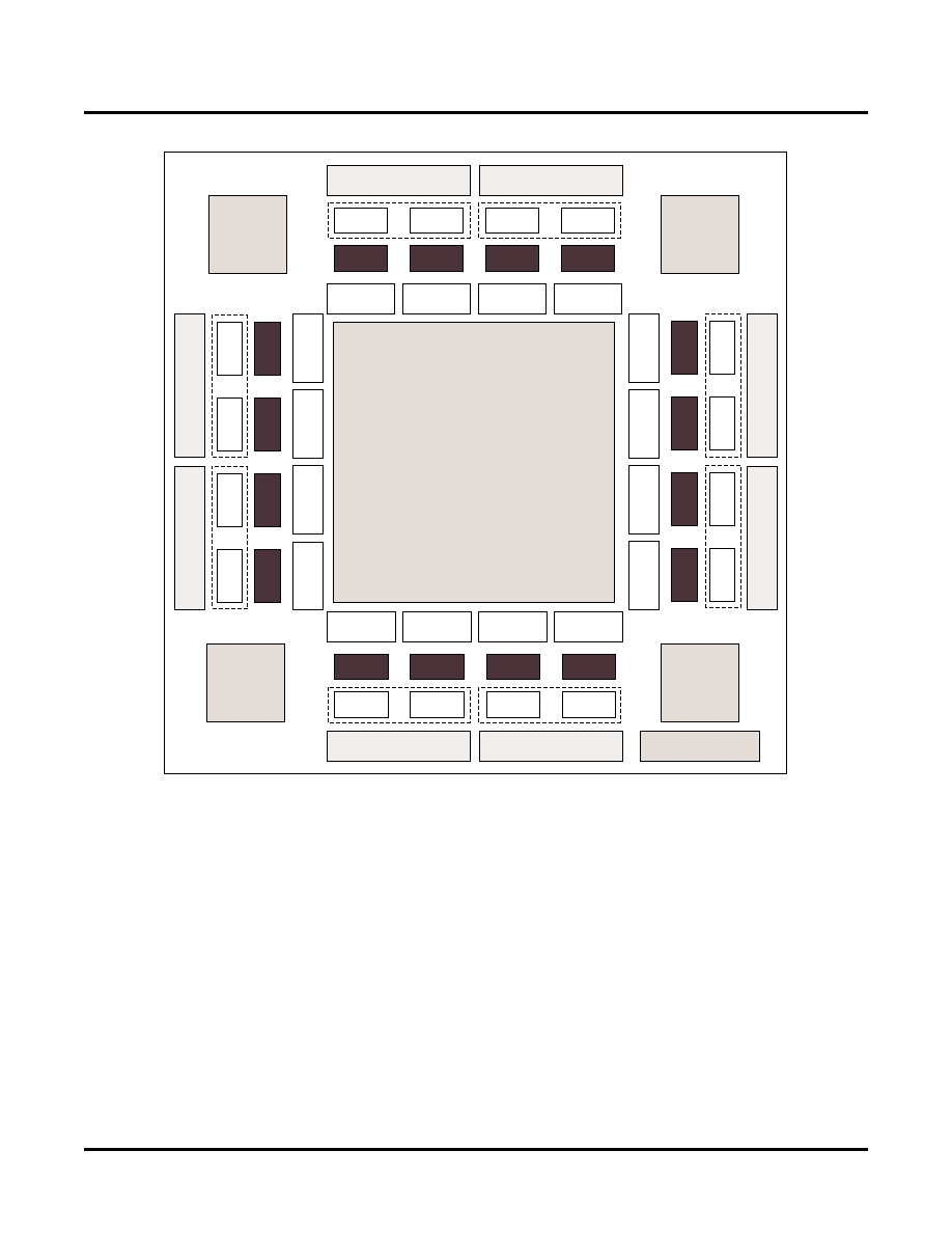
Figure 1. ispGDX2 Block Diagram (256-I/O Device)
This family of switches combines a flexible switching architecture with advanced sysIO interfaces including 850
Mbps sysHSI Blocks, and sysCLOCK PLLs to meet the needs of the today's high-speed systems. Through a muli-
plexer-intensive architecture, the ispGDX2 facilitates a variety of common switching functions.
The availability of on-chip control logic further enhances the power of these devices. A high-performance solution,
the family supports bandwidth up to 38Gbps.
Every device in the family has a number of PLLs to provide the system designer with the ability to generate multiple
clocks and manage clock skews in their systems.
The sysIO interfaces provide system-level performance and integration. These I/Os support various modes of
LVCMOS/LVTTL and support popular high-speed standard interfaces such as GTL+, PCI-X, HSTL, SSTL, LVDS
and Bus-LVDS. The sysHSI Blocks further extend this capability by providing high speed serial data transfer capa-
bility.
Devices in the family can operate at 3.3V, 2.5V or 1.8V core voltages and can be programmed in-system via an
IEEE 1149.1 interface that is compliant with the IEEE 1532 standard. Voltages required for the I/O buffers are inde-
pendent of the core voltage supply. This further enhances the flexibility of this family in system designs.
GDX Block
sysCLOCK
PLL
sysCLOCK
PLL
SERDES
sysIO Bank
sysIO Bank
sysIO Bank
sysIO Bank
SERDES
GDX Block
SERDES
GDX Block
SERDES
SERDES
SERDES
SERDES
SERDES
GDX Block
GDX Block
GDX Block
GDX Block
GDX Block
FIFO
FIFO
FIFO
FIFO
FIFO
FIFO
FIFO
FIFO
ISP & Boundary Scan
Test Port
GDX Bloc
k
SERDES
sysIO Bank
sysIO Bank
SERDES
GDX Bloc
k
SERDES
GDX Bloc
k
SERDES
GDX Bloc
k
FIFO
FIFO
FIFO
FIFO
sysIO Bank
sysIO Bank
SERDES
SERDES
SERDES
SERDES
GDX Bloc
k
GDX Bloc
k
GDX Bloc
k
GDX Bloc
k
FIFO
FIFO
FIFO
FIFO
sysHSI
Block
sysHSI
Block
sysHSI
Block
sysHSI
Block
sysHSI
Bloc
k
sysHSI
Bloc
k
sysHSI
Bloc
k
sysHSI
Bloc
k
sysCLOCK
PLL
sysCLOCK
PLL
Global Routing Pool
(GRP)

Lattice Semiconductor
ispGDX2V/B/C Family Data Sheet
3
Typical applications for the ispGDX2 include multi-port multi-processor interfaces, wide data and address bus mul-
tiplexing, programmable control signal routing and programmable bus interfaces. Table 1 shows the members of
the ispGDX2 family and their key features.
Architecture
The ispGDX2 devices consist of GDX Blocks interconnected by a Global Routing Pool (GRP). Signals interface
with the external system via sysIO banks. In addition, each GDX Block is associated with a FIFO and a sysHSI
Block to facilitate the transfer of data on- and off-chip. Figure 1 shows the ispGDX2 block diagram. Each GDX
Block can be individually configured in one of four modes:
∑ Basic (No FIFO or SERDES)
∑ FIFO Only
∑ SERDES Only
∑ SERDES and FIFO
Each sysIO bank has its own I/O power supply and reference voltage. Designers can use any output standard
within a bank that is compatible with the power supply. Any input standard may be used, providing it is compatible
with the reference voltage. The banks are independent.
Global Routing Pool (GRP)
The ispGDX2 architecture is organized into GDX Blocks, which are connected via a Global Routing Pool. The inno-
vative GRP is optimized for routability, flexibility and speed. All the signals enter via the GDX Block. The block sup-
plies these either directly or in registered form to the GRP. The GRP routes the signals to different blocks, and
provides separate data and control routing. The data path is optimized to achieve faster speed and routing flexibility
for nibble oriented signals. The control routing is optimized to provide high-speed bit oriented routing of control sig-
nals.
There are some restrictions on the allocation of pins for optimal bus routing. These restrictions are considered by
the software in the allocation of pins.
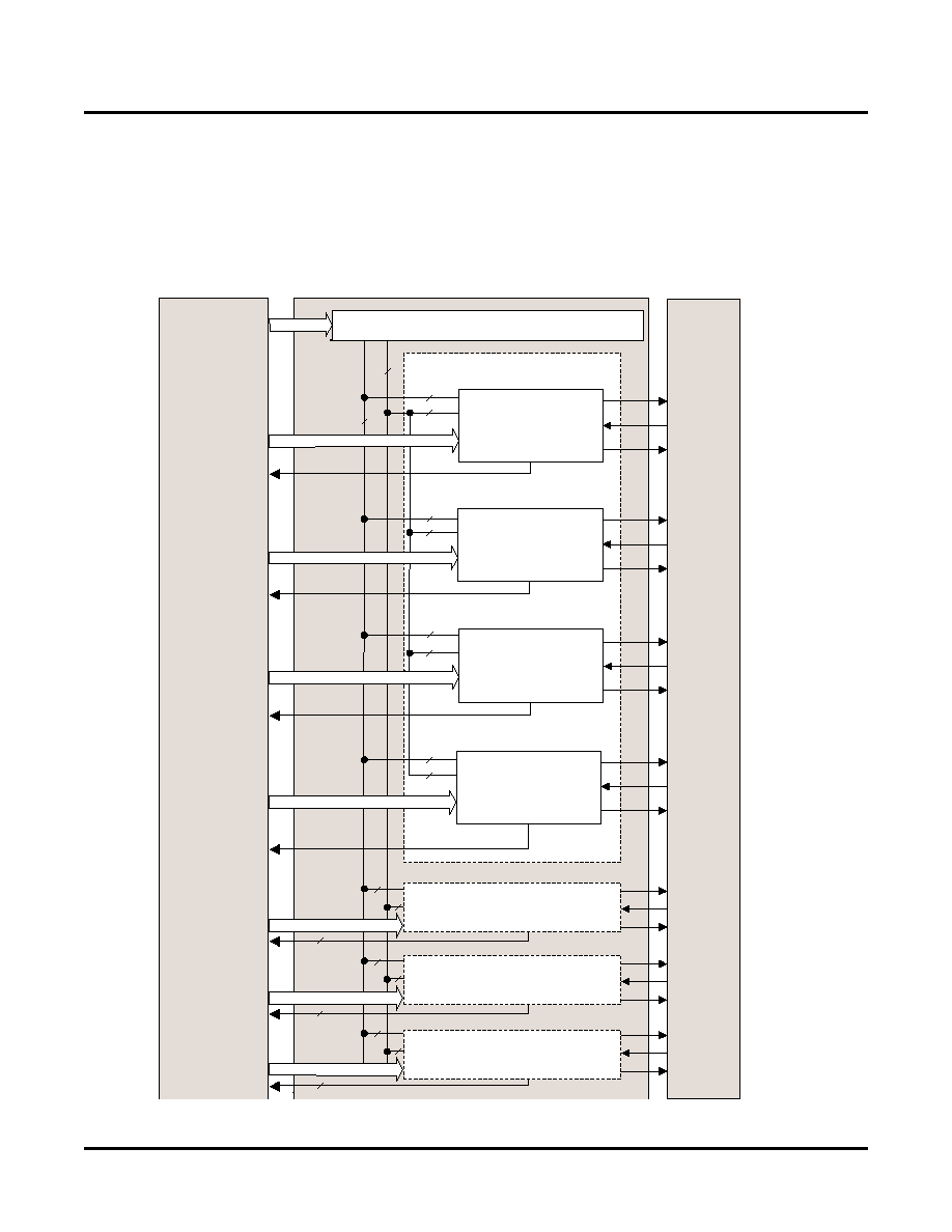
GDX Block
The blocks are organized in a "block" (nibble) manner, with each GDX Block providing data flow and control logic
for 16 I/O buffers. The data flow is organized as four nibbles, each nibble containing four Multiplexer Register
Blocks (MRBs). Data for the MRBs is provided from 64 lines from the GRP. Figure 2 illustrates the groups of signals
going into and out of a GDX Block.
Control signals for the MRBs are provided from the Control Array. The Control Array receives the 32 signals from
the GRP and generates 16 control signals: eight MUX Select, four Clock/Clock Enable, two Set/Reset and two Out-
put Enable. Each nibble is controlled via two MUX select signals. The remaining control signals go to all the MRBs.
Besides the control signals from the Control Array, the following global signals are available to the MRBs in each
GDX Block: four Clock/Clock Enable, one reset/preset, one power-on reset, two of four MUX select (two of two in
64 I/O), four Output Enable (two in 64 I/O) and Test Out Enable (TOE).
MUX and Register Block (MRB)
Every MRB Block has a 4:1 MUX (I/O MUX) and a set of three registers which are connected to the I/O buffers,
FIFO and sysHSI Blocks. Multiple MRBs can be combined to form large multiplexers as described below. Figure 3
shows the structure of the MRB.
Each of the three registers in the MRB can be configured as edge-triggered D-type flip-flop or as a level sensitive
latch. One register operates on the input data, the other output data and the last register synchronizes the output
enable function. The input and output data signals can bypass each of their registers. The polarity of the data out
and output enable signals can be selected.
Lattice Semiconductor
ispGDX2V/B/C Family Data Sheet
4
The Output and OE register share the same clock and clock enable signals. The Input register has a separate clock
and clock enable. The initialization signals of each register can be independently configured as Set or Reset. These
registers have programmable polarity control for Clock, Clock Enable and Set/Reset. The output enable register
input can be set either by one of the two output enables generated locally from the Control Array or from one of the
four (two in 64 I/O) Global OE enable pins. In addition to the local clock and clock enable signals, each MRB has
access to Global Clock, Clock Enable, Reset and TOE nets.
Figure 2. GDX Block
MUX and Register
Block (MRB)
0
OE
IN
OUT
OE
IN
OUT
OE
IN
OUT
OE
IN
OUT
OE
IN
OUT
OE
IN
OUT
OE
IN
OUT
MUX and Register
Block (MRB)
1
MUX and Register
Block (MRB)
2
GDX Block
GRP
sysIO Bank
32 bits
Control
MUX
Select
16 bits
16 bits
16 bits
4 bits
4 bits
4 bits
4 bits
8
2
MUX and Register
Block (MRB)
3
Control Array
8
2
2
8
2
8
2
8
2
8
8
8
8
2
4
4
4
Nibble 3
MRBs 12-15
Nibble 2
MRBs 8-11
Nibble 1
MRBs 4-7
Nibble 0

Lattice Semiconductor
ispGDX2V/B/C Family Data Sheet
5
The output register of the MRB has a built-in bi-directional shift register capability. Each output register correspond-
ing to MRB "n", receives data output from its two adjacent MRBs, MRB (n-1) and MRB (n+1), to provide shift regis-
ter capability. Like the output register, each input register of the MRB has built-in shift register capability. Each input
register can receive data from its two adjacent MRB input registers, to provide bi-directional shift register capability.
The chaining crosses GDX Block boundaries. The chain of input registers and the chain of output registers can be
combined as one shift register via the GRP.
The four data inputs to the 4:1 MUX come from the GRP. The output of this MUX connects to the output register. A
fast feedback path from the MUX to the GRP allows wider MUXes to be built. Table 2 summarizes the various MUX
sizes and delay levels.
Table 2. MUX Size Versus Internal Delay
Figure 3. ispGDX2 Family MRB
MUX Sizes
Levels of Internal GRP Delays
4:1
One Level
Up to 16:1
Two Levels
Up to 64:1
Three Levels
Up to 188:1 (with ispGDX2-256)
Four Levels
OE
Reg/Latch
OE
CE
CK
CK
CE
S/R
S/R
D/L
ClK
CE
Set
Reset
D/L
ClK
CE
Set
Reset
Q
Q
2
4
2
2-4
4
Set/Reset
CK/CE
CK/CE
OE
OE
to IN_Reg(n-1)
to IN_Reg(n+1)
from
Out_Reg(n-1)
from
Out_Reg(n+1)
FIFO Out*
from IN_Reg(n-1)
from IN_Reg(n+1)
to Out_Reg(n-1)
to Out_Reg(n+1)
Flags*
(FIFO, SERDES
or PLL)
*Selected MRBs see Logic Signal Connection Table for details
V
CC
V
CC
Delay
Global Resetb
Global Resetb
From GRP
MUX Select
Control Array Signals
MUX
Select
Global
Signals
Global
Signals
GDX
Control Array
TOE
To GRP
D/L
ClK
CE
Set
Reset
Q
Out
Reg/Latch
Input
Reg/Latch