Document Outline
- FEATURES
- GENERAL DESCRIPTION
- FUNCTIONAL DESCRIPTION
- ispMACH 4A TIMING MODEL
- SPEEDLOCKING FOR GUARANTEED FIXED TIMING
- IEEE 1149.1-COMPLIANT BOUNDARY SCAN TESTABILITY
- IEEE 1149.1-COMPLIANT IN-SYSTEM PROGRAMMING
- PCI COMPLIANT
- SAFE FOR MIXED SUPPLY VOLTAGE SYSTEM DESIGNS
- PULL UP OR BUS-FRIENDLY INPUTS AND I/Os
- POWER MANAGEMENT
- PROGRAMMABLE SLEW RATE
- POWER-UP RESET/SET
- SECURITY BIT
- HOT SOCKETING
- BLOCK DIAGRAM Ö M4A(3,5)-32/32
- BLOCK DIAGRAM Ö M4A(3,5)-64/32
- BLOCK DIAGRAM Ö M4A3-64/64
- BLOCK DIAGRAM Ö M4A(3,5)-96/48
- BLOCK DIAGRAM Ö M4A(3,5)-128/64
- BLOCK DIAGRAM Ö M4A(3,5)-192/96
- BLOCK DIAGRAM Ö M4A(3,5)-256/128
- BLOCK DIAGRAM Ö M4A3-256/160, M4A3-256/192
- BLOCK DIAGRAM Ö M4A3-384/160, M4A3-384/192
- BLOCK DIAGRAM - M4A3-512/160, M4A3-512/192, M4A3-512/256
- ABSOLUTE MAXIMUM RATINGS
- OPERATING RANGES
- 5-V DC CHARACTERISTICS OVER OPERATING RANGES
- ABSOLUTE MAXIMUM RATINGS
- OPERATING RANGES
- 3.3-V DC CHARACTERISTICS OVER OPERATING RANGES
- ispMACH 4A TIMING PARAMETERS OVER OPERATING RANGES1 �
- CAPACITANCE 1
- ICC vs. FREQUENCY
- 44-PIN PLCC CONNECTION DIAGRAM (M4A(3,5)-32/32 AND M4A(3,5)-64/32)
- 44-PIN TQFP CONNECTION DIAGRAM (M4A(3,5)-32/32 AND M4A(3,5)-64/32)
- 48-PIN TQFP CONNECTION DIAGRAM (M4A(3,5)-32/32 AND M4A(3,5)-64/32)
- 100-PIN TQFP CONNECTION DIAGRAM (M4A(3,5)-96/48)
- 100-PIN PQFP CONNECTION DIAGRAM (M4A(3,5)-128/64)
- 100-PIN TQFP CONNECTION DIAGRAM (M4A3-64/64 AND M4A(3,5)-128/64)
- 100-BALL caBGA CONNECTION DIAGRAM (M4A3-128/64)
- 144-PIN TQFP CONNECTION DIAGRAM (M4A(3,5)-192/96)
- 144-BALL fpBGA CONNECTION DIAGRAM (M4A3-192/96)
- 208-PIN PQFP CONNECTION DIAGRAM (M4A(3,5)-256/128 AND M4A3-256/160)
- 208-PIN PQFP CONNECTION DIAGRAM (M4A3-384/160 AND M4A3-512/160)
- 256-BALL BGA CONNECTION DIAGRAM (M4A3-256/128)
- 256-BALL fpBGA CONNECTION DIAGRAM (M4A3-256/192)
- 256-BALL BGA CONNECTION DIAGRAM - (M4A3-384/192)
- 256-BALL fpBGA CONNECTION DIAGRAM (M4A3-256/128)
- 256-BALL fpBGA CONNECTION DIAGRAM (M4A3-384/192)
- 256-BALL fpBGA CONNECTION DIAGRAM (M4A3-512/192)
- 388-BALL fpBGA CONNECTION DIAGRAM (M4A3-512/256)
- ispMACH 4A PRODUCT ORDERING INFORMATION
Publication#
ISPM4A
Rev:
J
Amendment/
0
Issue Date:
February 2003
ispMACH
TM
4A CPLD Family
High Performance E
2
CMOS
Æ
In-System Programmable Logic
FEATURES
High-performance, E
2
CMOS 3.3-V & 5-V CPLD families
Flexible architecture for rapid logic designs
-- Excellent First-Time-Fit
TM
and refit feature
-- SpeedLocking
TM
performance for guaranteed fixed timing
-- Central, input and output switch matrices for 100% routability and 100% pin-out retention
High speed
-- 5.0ns t
PD
Commercial and 7.5ns t
PD
Industrial
-- 182MHz f
CNT
32 to 512 macrocells; 32 to 768 registers
44 to 388 pins in PLCC, PQFP, TQFP, BGA, fpBGA and caBGA packages
Flexible architecture for a wide range of design styles
-- D/T registers and latches
-- Synchronous or asynchronous mode
-- Dedicated input registers
-- Programmable polarity
-- Reset/ preset swapping
Advanced capabilities for easy system integration
-- 3.3-V & 5-V JEDEC-compliant operations
-- JTAG (IEEE 1149.1) compliant for boundary scan testing
-- 3.3-V & 5-V JTAG in-system programming
-- PCI compliant (-5/-55/-6/-65/-7/-10/-12 speed grades)
-- Safe for mixed supply voltage system designs
-- Programmable pull-up or Bus-Friendly
TM
inputs and I/Os
-- Hot-socketing
-- Programmable security bit
-- Individual output slew rate control
Advanced E
2
CMOS process provides high-performance, cost-effective solutions
2
ispMACH 4A Family
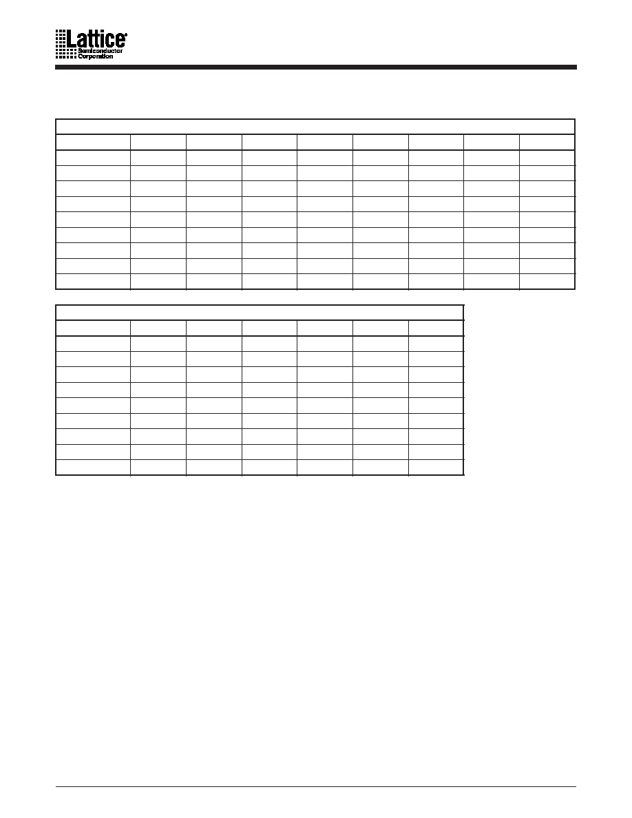
Table 1. ispMACH 4A Device Features
3.3 V Devices
Feature
M4A3-32
M4A3-64
M4A3-96
M4A3-128
M4A3-192
M4A3-256
M4A3-384
M4A3-512
Macrocells
32
64
96
128
192
256
384
512
User I/O options
32
32/64
48
64
96
128/160/192
160/192
160/192/256
t
PD
(ns)
5.0
5.5
5.5
5.5
6.0
5.5
6.5
7.5
f
CNT
(MHz)
182
167
167
167
160
167
154
125
t
COS
(ns)
4.0
4.0
4.0
4.0
4.5
4.0
4.5
5.5
t
SS
(ns)
3.0
3.5
3.5
3.5
3.5
3.5
3.5
5.0
Static Power (mA)
20
25/52
40
55
85
110/150
149/155
179
JTAG Compliant
Yes
Yes
Yes
Yes
Yes
Yes
Yes
Yes
PCI Compliant
Yes
Yes
Yes
Yes
Yes
Yes
Yes
Yes
5 V Devices
Feature
M4A5-32
M4A5-64
M4A5-96
M4A5-128
M4A5-192
M4A5-256
Macrocells
32
64
96
128
192
256
User I/O options
32
32
48
64
96
128
t
PD
(ns)
5.0
5.5
5.5
5.5
6.0
6.5
f
CNT
(MHz)
182
167
167
167
160
154
t
COS
(ns)
4.0
4.0
4.0
4.0
4.5
5.0
t
SS
(ns)
3.0
3.5
3.5
3.5
3.5
3.5
Static Power (mA)
20
25
40
55
74
110
JTAG Compliant
Yes
Yes
Yes
Yes
Yes
Yes
PCI Compliant
Yes
Yes
Yes
Yes
Yes
Yes
ispMACH 4A Family
3
GENERAL DESCRIPTION
The ispMACH
TM
4A family from Lattice offers an exceptionally flexible architecture and delivers
a superior Complex Programmable Logic Device (CPLD) solution of easy-to-use silicon products
and software tools. The overall benefits for users are a guaranteed and predictable CPLD
solution, faster time-to-market, greater flexibility and lower cost. The ispMACH 4A devices offer
densities ranging from 32 to 512 macrocells with 100% utilization and 100% pin-out retention.
The ispMACH 4A families offer 5-V (M4A5-xxx) and 3.3-V (M4A3-xxx) operation.
ispMACH 4A products are 5-V or 3.3-V in-system programmable through the JTAG (IEEE Std.
1149.1) interface. JTAG boundary scan testing also allows product testability on automated test
equipment for device connectivity.
All ispMACH 4A family members deliver First-Time-Fit and easy system integration with pin-out
retention after any design change and refit. For both 3.3-V and 5-V operation, ispMACH 4A
products can deliver guaranteed fixed timing as fast as 5.0 ns t
PD
and 182 MHz f
CNT
through the
SpeedLocking feature when using up to 20 product terms per output (Table 2).
Note:
1. C = Commercial, I = Industrial
Table 2. ispMACH 4A Speed Grades
Device
Speed Grade
-5
-55
-6
-65
-7
-10
-12
-14
M4A3-32
M4A5-32
C
C, I
C, I
I
M4A3-64/32
M4A5-64/32
C
C, I
C, I
I
M4A3-64/64
C
C, I
C, I
I
M4A3-96
M4A5-96
C
C, I
C, I
I
M4A3-128
M4A5-128
C
C, I
C, I
I
M4A3-192
M4A5-192
C
C, I
C, I
I
M4A3-256/128
C
C
C, I
C, I
I
M4A5-256/128
C
C
C, I
I
M4A3-256/192
M4A3-256/160
C
C, I
I
M4A3-384
C
C, I
C, I
I
M4A3-512
C
C, I
C, I
I
4
ispMACH 4A Family
The ispMACH 4A family offers 20 density-I/O combinations in Thin Quad Flat Pack (TQFP),
Plastic Quad Flat Pack (PQFP), Plastic Leaded Chip Carrier (PLCC), Ball Grid Array (BGA), fine-
pitch BGA (fpBGA), and chip-array BGA (caBGA) packages ranging from 44 to 388 pins (Table
3). It also offers I/O safety features for mixed-voltage designs so that the 3.3-V devices can accept
5-V inputs, and 5-V devices do not overdrive 3.3-V inputs. Additional features include Bus-
Friendly inputs and I/Os, a programmable power-down mode for extra power savings and
individual output slew rate control for the highest speed transition or for the lowest noise
transition.
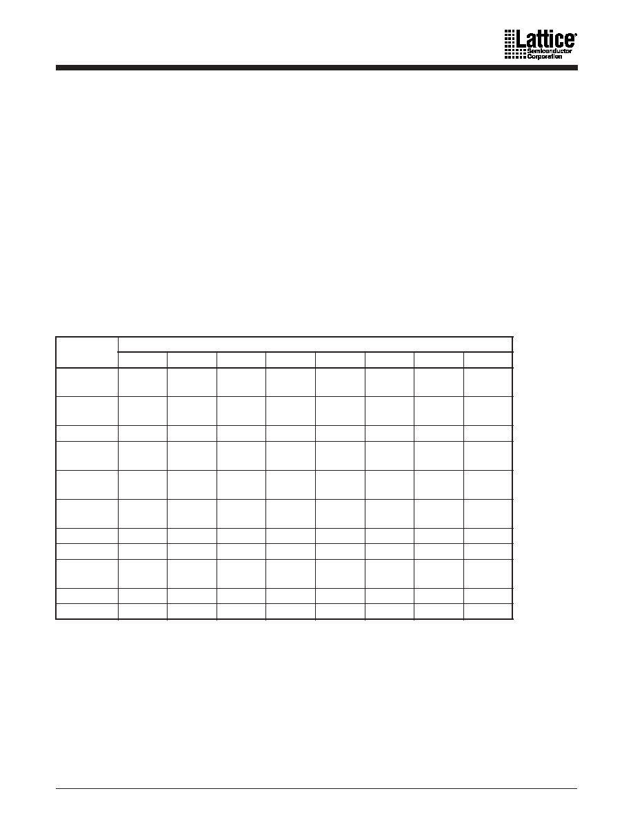
Table 3. ispMACH 4A Package and I/O Options
(Number of I/Os and dedicated inputs in Table)
3.3 V Devices
Package
M4A3-32
M4A3-64
M4A3-96
M4A3-128
M4A3-192
M4A3-256
M4A3-384
M4A3-512
44-pin PLCC
32+2
32+2
44-pin TQFP
32+2
32+2
48-pin TQFP
32+2
32+2
100-pin TQFP
64+6
48+8
64+6
100-pin PQFP
64+6
100-ball caBGA
64+6
144-pin TQFP
96+16
144-ball fpBGA
96+16
208-pin PQFP
128+14, 160
160
160
256-ball fpBGA
128+14, 192
192
192
256-ball BGA
128+14
192
388-ball fpBGA
256
5 V Devices
Package
M4A5-32
M4A5-64
M4A5-96
M4A5-128
M4A5-192
M4A5-256
44-pin PLCC
32+2
32+2
44-pin TQFP
32+2
32+2
48-pin TQFP
32+2
32+2
100-pin TQFP
48+8
64+6
100-pin PQFP
64+6
144-pin TQFP
96+16
208-pin PQFP
128+14
256-ball BGA
128+14

ispMACH 4A Family
5
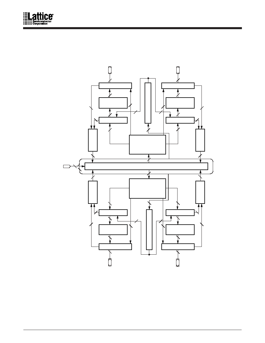
FUNCTIONAL DESCRIPTION
The fundamental architecture of ispMACH 4A devices (Figure 1) consists of multiple, optimized
PAL
Æ
blocks interconnected by a central switch matrix. The central switch matrix allows
communication between PAL blocks and routes inputs to the PAL blocks. Together, the PAL
blocks and central switch matrix allow the logic designer to create large designs in a single
device instead of having to use multiple devices.
The key to being able to make effective use of these devices lies in the interconnect schemes.
In the ispMACH 4A architecture, the macrocells are flexibly coupled to the product terms
through the logic allocator, and the I/O pins are flexibly coupled to the macrocells due to the
output switch matrix. In addition, more input routing options are provided by the input switch
matrix. These resources provide the flexibility needed to fit designs efficiently.
Notes:
1. 16 for ispMACH 4A devices with 1:1 macrocell-I/O cell ratio (see next page).
2. Block clocks do not go to I/O cells in M4A(3,5)-32/32.
3. M4A(3,5)-192, M4A(3,5)-256, M4A3-384, and M4A3-512 have dedicated clock pins which cannot be used as inputs and do
not connect to the central switch matrix.
I/O
Pins
Clock/Input
Pins
Central Switch Matrix
I/O
Pins
I/O
Pins
Dedicated
Input Pins
PAL Block
PAL Block
Logic
Allocator
with XOR
Output/
Buried
Macrocells
33/
34/
36
16
16
Clock
Generator
Logic
Array
Output Switch Matrix
Input
Switch
Matrix
I/O Cells
16
16
8
Note 1
Note 2
Note 3
4
PAL Block
17466G-001
Figure 1. ispMACH 4A Block Diagram and PAL Block Structure

6
ispMACH 4A Family
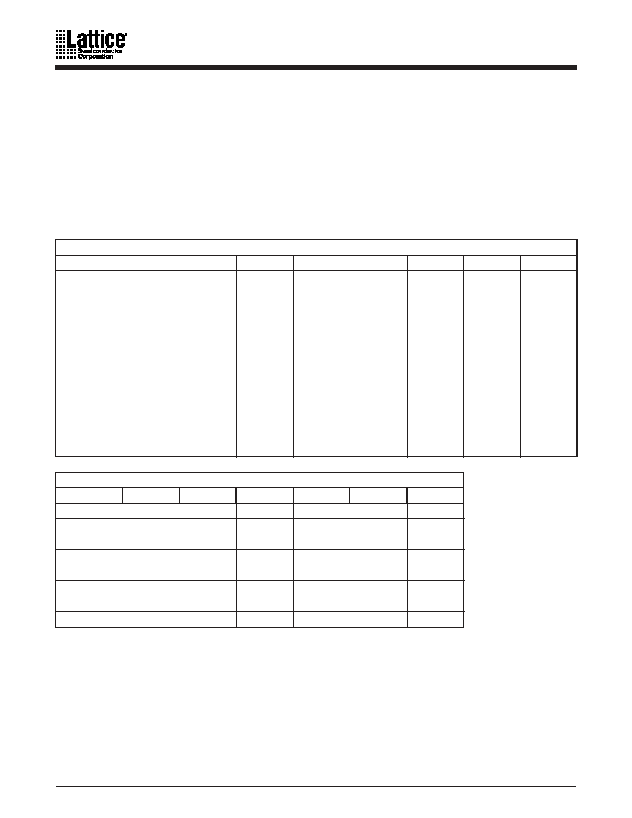
Table 4. Architectural Summary of ispMACH 4A devices
The Macrocell-I/O cell ratio is defined as the number of macrocells versus the number of I/O
cells internally in a PAL block (Table 4).
The central switch matrix takes all dedicated inputs and signals from the input switch matrices
and routes them as needed to the PAL blocks. Feedback signals that return to the same PAL block
still must go through the central switch matrix. This mechanism ensures that PAL blocks in
ispMACH 4A devices communicate with each other with consistent, predictable delays.
The central switch matrix makes a ispMACH 4A device more advanced than simply several PAL
devices on a single chip. It allows the designer to think of the device not as a collection of
blocks, but as a single programmable device; the software partitions the design into PAL blocks
through the central switch matrix so that the designer does not have to be concerned with the
internal architecture of the device.
Each PAL block consists of:
Product-term array
Logic allocator
Macrocells
Output switch matrix
I/O cells
Input switch matrix
Clock generator
Notes:
1. M4A3-64/64 internal switch matrix functionality embedded in central switch matrix.
ispMACH 4A Devices
M4A3-64/32, M4A5-64/32
M4A3-96/48, M4A5-96/48
M4A3-128/64, M4A5-128/64
M4A3-192/96, M4A5-192/96
M4A3-256/128, M4A5-256/128
M4A3-384
M4A3-512
M4A3-32/32
M4A5-32/32
M4A3-64/64
M4A3-256/160
M4A3-256/192
Macrocell-I/O Cell
Ratio
2:1
1:1
Input Switch Matrix
Yes
Yes
1
Input Registers
Yes
No
Central Switch Matrix
Yes
Yes
Output Switch Matrix
Yes
Yes

ispMACH 4A Family
7
Product-Term Array
The product-term array consists of a number of product terms that form the basis of the logic
being implemented. The inputs to the AND gates come from the central switch matrix (Table 5),
and are provided in both true and complement forms for efficient logic implementation.
Logic Allocator
Within the logic allocator, product terms are allocated to macrocells in "product term clusters."
The availability and distribution of product term clusters are automatically considered by the
software as it fits functions within a PAL block. The size of a product term cluster has been
optimized to provide high utilization of product terms, making complex functions using many
product terms possible. Yet when few product terms are used, there will be a minimal number
of unused--or wasted--product terms left over. The product term clusters available to each
macrocell within a PAL block are shown in Tables 6 and 7.
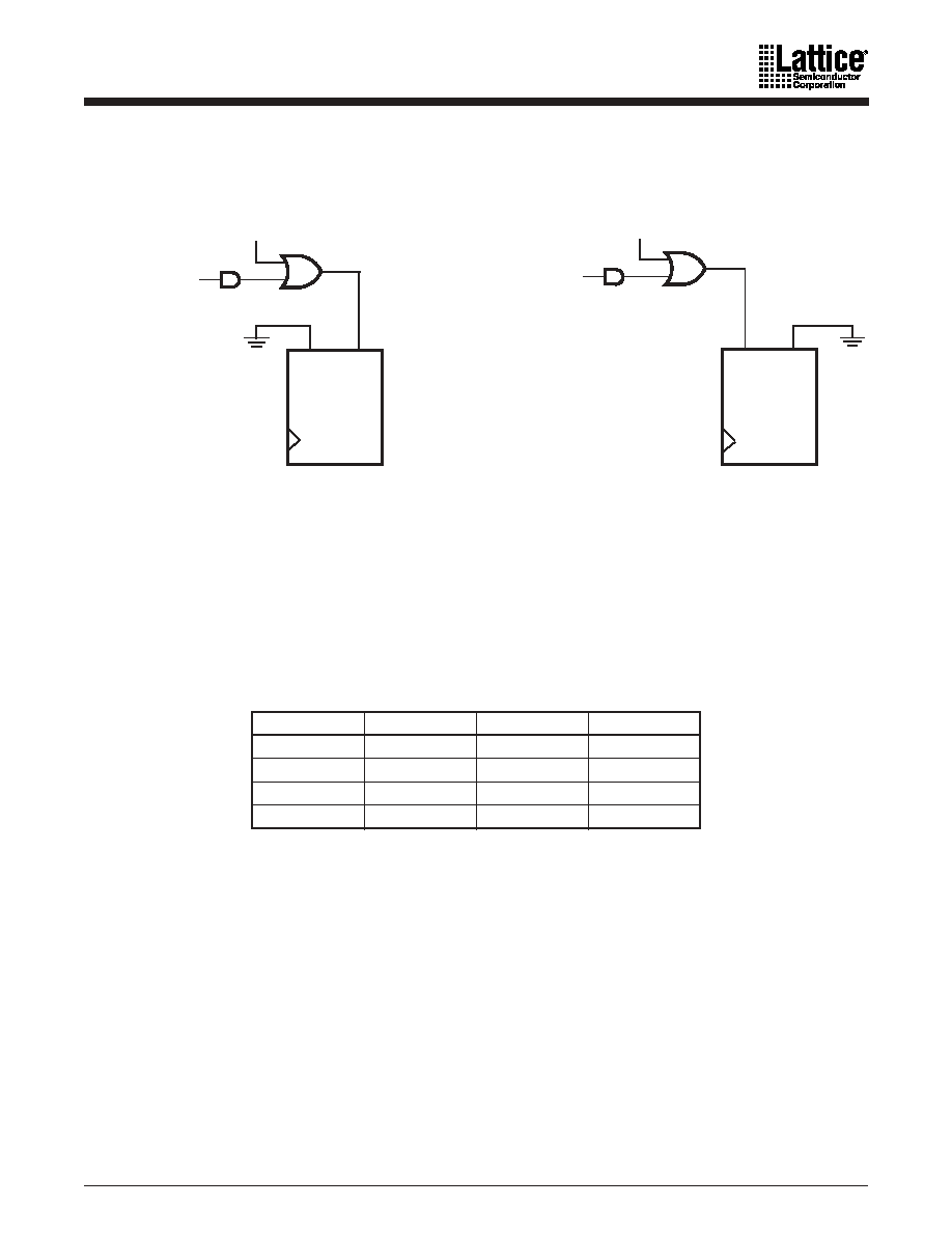
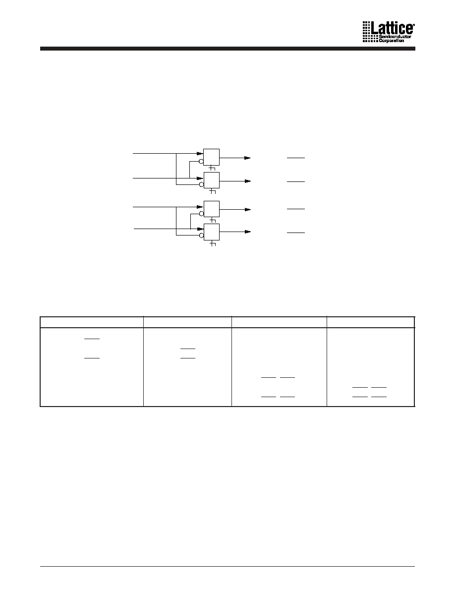
Each product term cluster is associated with a macrocell. The size of a cluster depends on the
configuration of the associated macrocell. When the macrocell is used in synchronous mode
(Figure 2a), the basic cluster has 4 product terms. When the associated macrocell is used in
asynchronous mode (Figure 2b), the cluster has 2 product terms. Note that if the product term
cluster is routed to a different macrocell, the allocator configuration is not determined by the
mode of the macrocell actually being driven. The configuration is always set by the mode of the
macrocell that the cluster will drive if not routed away, regardless of the actual routing.
In addition, there is an extra product term that can either join the basic cluster to give an
extended cluster, or drive the second input of an exclusive-OR gate in the signal path. If included
with the basic cluster, this provides for up to 20 product terms on a synchronous function that
uses four extended 5-product-term clusters. A similar asynchronous function can have up to 18
product terms.
When the extra product term is used to extend the cluster, the value of the second XOR input
can be programmed as a 0 or a 1, giving polarity control. The possible configurations of the logic
allocator are shown in Figures 3 and 4.
Table 5. PAL Block Inputs
Device
Number of Inputs to PAL Block
M4A3-32/32 and M4A5-32/32
M4A3-64/32 and M4A5-64/32
M4A3-64/64
M4A3-96/48 and M4A5-96/48
M4A3-128/64 and M4A5-128/64
33
33
33
33
33
M4A3-192/96 and M4A5-192/96
M4A3-256/128 and M4A5-256/128
34
34
M4A3-256/160 and M4A3-256/192
M4A3-384
M4A3-512
36
36
36

8
ispMACH 4A Family
Table 6. Logic Allocator for All ispMACH 4A Devices (except M4A(3,5)-32/32)
Output Macrocell
Available Clusters
Output Macrocell
Available Clusters
M
0
C
0
, C
1
, C
2
M
8
C
7
,
C
8
, C
9
, C
10
M
1
C
0
, C
1
, C
2
, C
3
M
9
C
8
, C
9
, C
10
, C
11
M
2
C
1
, C
2
, C
3
, C
4
M
10
C
9
, C
10
, C
11
, C
12
M
3
C
2
, C
3
, C
4
, C
5
M
11
C
10
, C
11
, C
12
, C
13
M
4
C
3
, C
4
, C
5
, C
6
M
12
C
11
, C
12
, C
13
, C
14
M
5
C
4
, C
5
, C
6
, C
7
M
13
C
12
, C
13
, C
14
, C
15
M
6
C
5
, C
6
, C
7
,
C
8
M
14
C
13
, C
14
, C
15
M
7
C
6
, C
7
,
C
8
, C
9
M
15
C
14
, C
15
Table 7. Logic Allocator for M4A(3,5)-32/32
Output Macrocell
Available Clusters
Output Macrocell
Available Clusters
M
0
C
0
, C
1
, C
2
M
8
C
8
, C
9
, C
10
M
1
C
0
, C
1
, C
2
, C
3
M
9
C
8
, C
9
, C
10
, C
11
M
2
C
1
, C
2
, C
3
, C
4
M
10
C
9
, C
10
, C
11
, C
12
M
3
C
2
, C
3
, C
4
, C
5
M
11
C
10
, C
11
, C
12
, C
13
M
4
C
3
, C
4
, C
5
, C
6
M
12
C
11
, C
12
, C
13
, C
14
M
5
C
4
, C
5
, C
6
, C
7
M
13
C
12
, C
13
, C
14
, C
15
M
6
C
5
, C
6
, C
7
M
14
C
13
, C
14
, C
15
M
7
C
6
, C
7
M
15
C
14
, C
15
0 Default
0 Default
Prog. Polarity
To n-1
To n-2
From n-1
To n+1
From n+1
From n+2
Basic Product
Term Cluster
Extra
Product
Term
Logic Allocator
n
n
To Macrocell
n
0 Default
0 Default
Prog. Polarity
To n-1
To n-2
From n-1
To n+1
From n+1
From n+2
Basic Product
Term Cluster
Extra
Product
Term
Logic Allocator
n
n
To Macrocell
n
17466G-006
Figure 2. Logic Allocator: Configuration of Cluster "n" Set by Mode of Macrocell "n"
17466G-005
a. Synchronous Mode
b. Asynchronous Mode
ispMACH 4A Family
9
Note that the configuration of the logic allocator has absolutely no impact on the speed of the
signal. All configurations have the same delay. This means that designers do not have to decide
between optimizing resources or speed; both can be optimized.
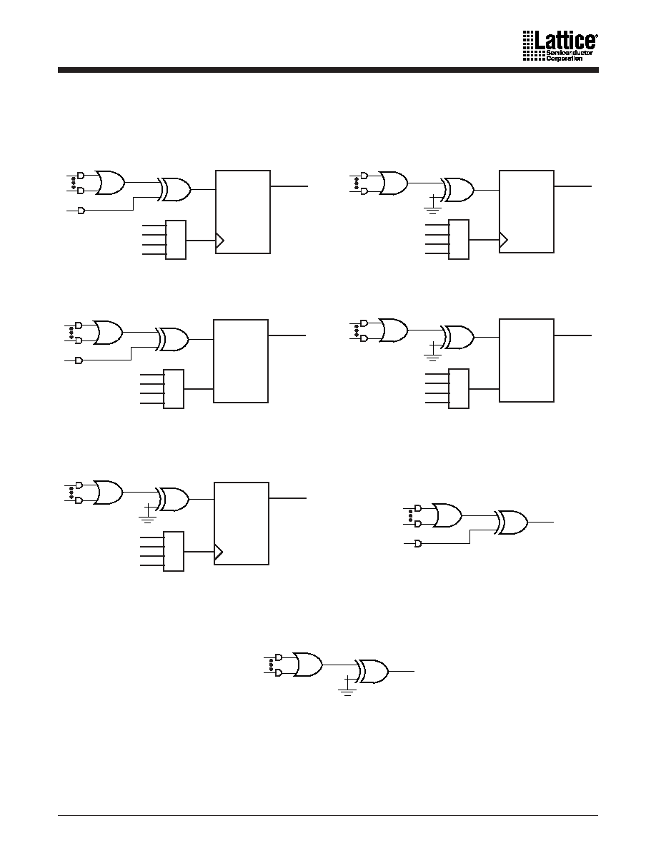
If not used in the cluster, the extra product term can act in conjunction with the basic cluster to
provide XOR logic for such functions as data comparison, or it can work with the D-,T-type flip-
flop to provide for J-K, and S-R register operation. In addition, if the basic cluster is routed to
another macrocell, the extra product term is still available for logic. In this case, the first XOR
input will be a logic 0. This circuit has the flexibility to route product terms elsewhere without
giving up the use of the macrocell.
Product term clusters do not "wrap" around a PAL block. This means that the macrocells at the
ends of the block have fewer product terms available.
0
17466G-007
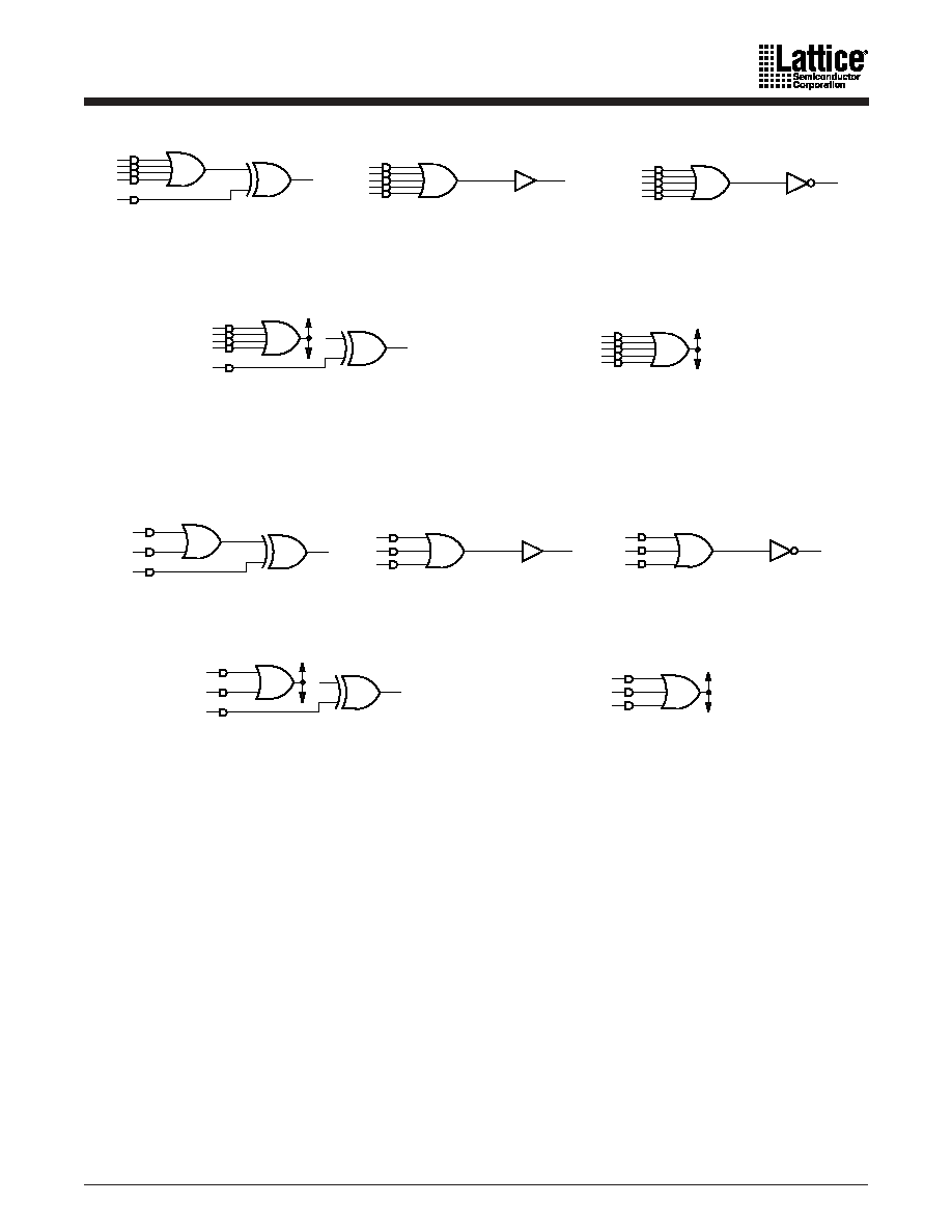
Figure 3. Logic Allocator Configurations: Synchronous Mode
a. Basic cluster with XOR
b. Extended cluster, active high
c. Extended cluster, active low
d. Basic cluster routed away;
single-product-term, active high
e. Extended cluster routed away
0
17466G-008
Figure 4. Logic Allocator Configurations: Asynchronous Mode
b. Extended cluster, active high
c. Extended cluster, active low
e. Extended cluster routed away
d. Basic cluster routed away;
single-product-term, active high
a. Basic cluster with XOR
10
ispMACH 4A Family
Macrocell
The macrocell consists of a storage element, routing resources, a clock multiplexer, and
initialization control. The macrocell has two fundamental modes: synchronous and
asynchronous (Figure 5). The mode chosen only affects clocking and initialization in the
macrocell.
In either mode, a combinatorial path can be used. For combinatorial logic, the synchronous
mode will generally be used, since it provides more product terms in the allocator.
SWAP
D/T/L
Q
AP
AR
Power-Up
Reset
PAL-Block
Initialization
Product Terms
From Logic Allocator
Block CLK0
Block CLK1
Block CLK2
Block CLK3
To Output and Input
Switch Matrices
Common PAL-block resource
Individual macrocell resources
From
PAL-Clock
Generator
D/T/L
Q
AP
AR
Power-Up
Reset
Individual
Initialization
Product Term
From Logic
Allocator
Block CLK0
Block CLK1
To Output and Input
Switch Matrices
Individual Clock
Product Term
From PAL-Block
Clock Generator
SWAP
17466G-010
Figure 5. Macrocell
17466G-009
a. Synchronous mode
b. Asynchronous mode
ispMACH 4A Family
11
The flip-flop can be configured as a D-type or T-type latch. J-K or S-R registers can be
synthesized. The primary flip-flop configurations are shown in Figure 6, although others are
possible. Flip-flop functionality is defined in Table 8. Note that a J-K latch is inadvisable as it will
cause oscillation if both J and K inputs are HIGH.
D
Q
AP AR
D
Q
AP AR
L
Q
AP AR
L
Q
AP AR
G
G
T
Q
AP AR
17466G-011
Figure 6. Primary Macrocell Configurations
g. Combinatorial with programmable polarity
a. D-type with XOR
b. D-type with programmable D polarity
c. Latch with XOR
d. Latch with programmable D polarity
e. T-type with programmable T polarity
f. Combinatorial with XOR
12
ispMACH 4A Family
Note:
1. Polarity of CLK/LE can be programmed
Although the macrocell shows only one input to the register, the XOR gate in the logic allocator
allows the D-, T-type register to emulate J-K, and S-R behavior. In this case, the available product
terms are divided between J and K (or S and R). When configured as J-K, S-R, or T-type, the
extra product term must be used on the XOR gate input for flip-flop emulation. In any register
type, the polarity of the inputs can be programmed.
The clock input to the flip-flop can select any of the four PAL block clocks in synchronous mode,
with the additional choice of either polarity of an individual product term clock in the
asynchronous mode.
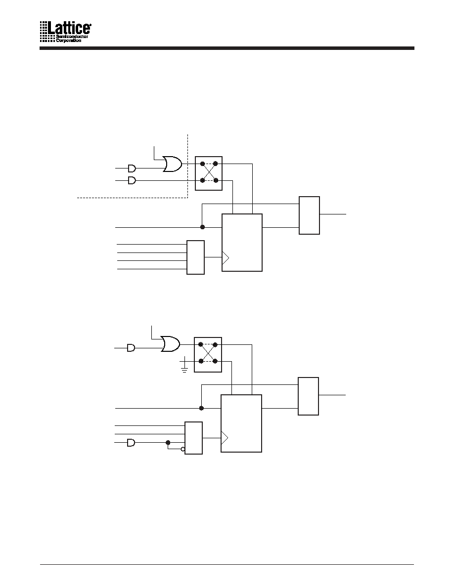
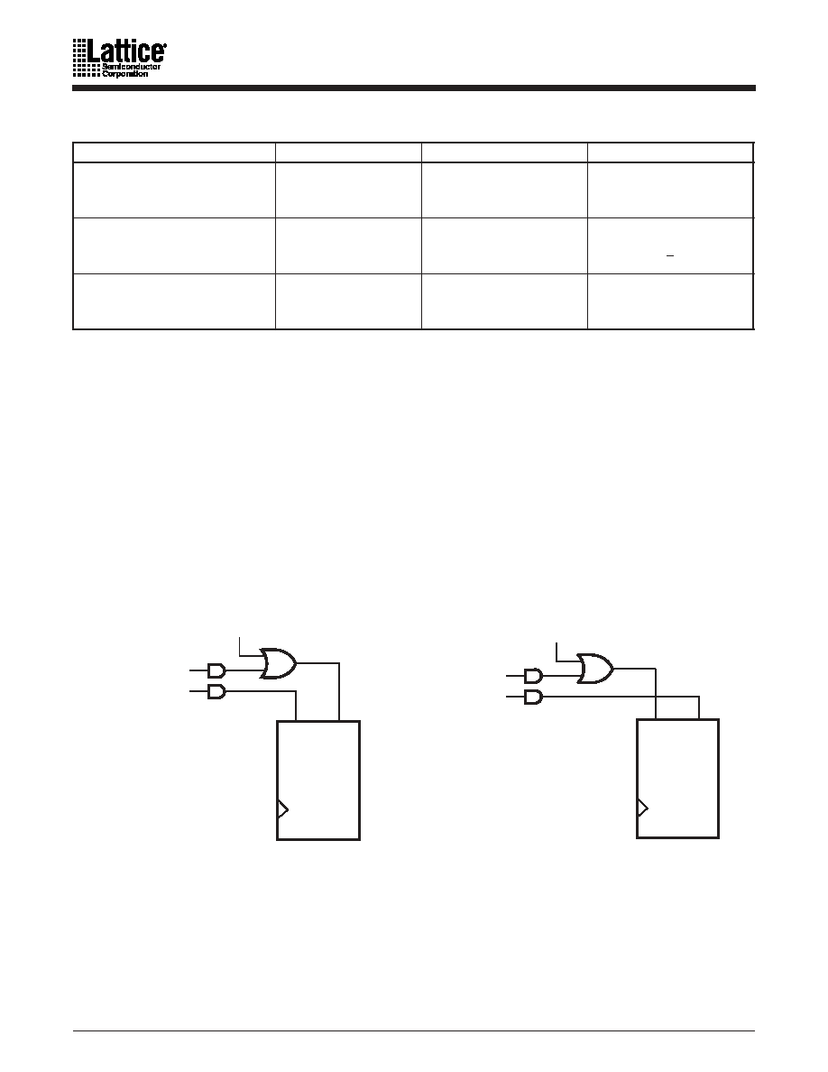
The initialization circuit depends on the mode. In synchronous mode (Figure 7), asynchronous
reset and preset are provided, each driven by a product term common to the entire PAL block.
Table 8. Register/Latch Operation
Configuration
Input(s)
CLK/LE
1
Q+
D-type Register
D=X
D=0
D=1
0,1, ()
()
()
Q
0
1
T-type Register
T=X
T=0
T=1
0, 1, ()
()
()
Q
Q
Q
D-type Latch
D=X
D=0
D=1
1(0)
0(1)
0(1)
Q
0
1
Power-Up
Reset
AP
D/T/L
AR
Q
PAL-Block
Initialization
Product Terms
a. Power-up reset
Power-Up
Preset
AP
D/L
PAL-Block
Initialization
Product Terms
AR
Q
17466G-012
17466G-013
Figure 7. Synchronous Mode Initialization Configurations
b. Power-up preset
ispMACH 4A Family
13
A reset/preset swapping feature in each macrocell allows for reset and preset to be exchanged,
providing flexibility. In asynchronous mode (Figure 8), a single individual product term is
provided for initialization. It can be selected to control reset or preset.
Note that the reset/preset swapping selection feature effects power-up reset as well. The
initialization functionality of the flip-flops is illustrated in Table 9. The macrocell sends its data
to the output switch matrix and the input switch matrix. The output switch matrix can route this
data to an output if so desired. The input switch matrix can send the signal back to the central
switch matrix as feedback.
Note:
1. Transparent latch is unaffected by AR, AP
Table 9. Asynchronous Reset/Preset Operation
AR
AP
CLK/LE
1
Q+
0
0
X
See Table 8
0
1
X
1
1
0
X
0
1
1
X
0
Power-Up
Reset
AP
D/L/T
AR
Q
Individual
Reset
Product Term
a. Reset
Power-Up
Preset
AP
D/L/T
AR
Q
Individual
Preset
Product Term
b. Preset
17466G-014
17466G-015
Figure 8. Asynchronous Mode Initialization Configurations
14
ispMACH 4A Family
Output Switch Matrix
The output switch matrix allows macrocells to be connected to any of several I/O cells within a
PAL block. This provides high flexibility in determining pinout and allows design changes to
occur without effecting pinout.
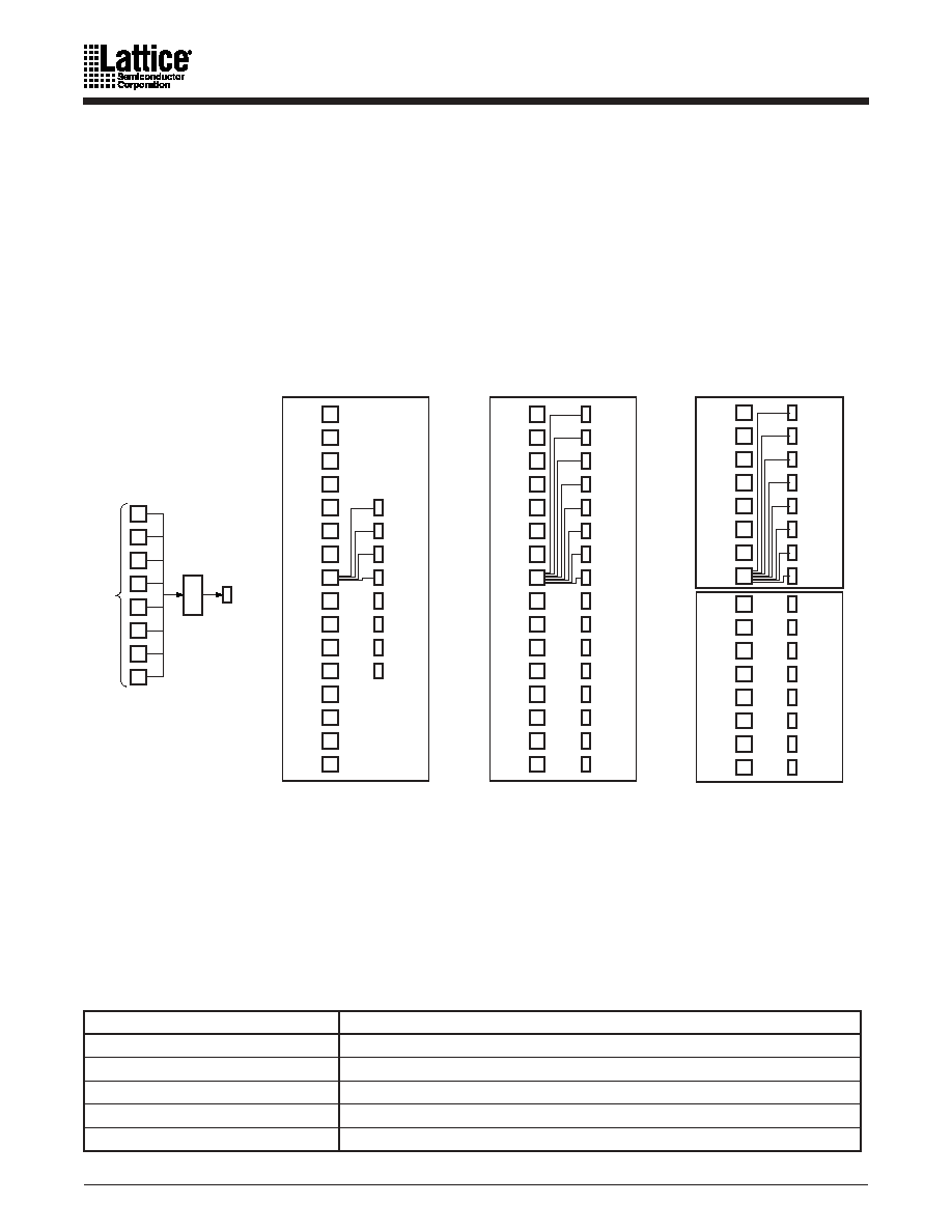
In ispMACH 4A devices with 2:1 Macrocell-I/O cell ratio, each PAL block has twice as many
macrocells as I/O cells. The ispMACH 4A output switch matrix allows for half of the macrocells
to drive I/O cells within a PAL block, in combinations according to Figure 9. Each I/O cell can
choose from eight macrocells; each macrocell has a choice of four I/O cells. The ispMACH 4A
devices with 1:1 Macrocell-I/O cell ratio allow each macrocell to drive one of eight I/O cells
(Figure 9).
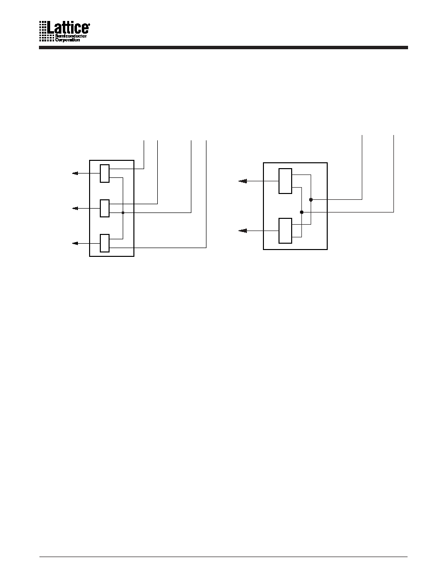
Table 10. Output Switch Matrix Combinations for ispMACH 4A Devices with 2:1 Macrocell-I/O Cell Ratio
Macrocell
Routable to I/O Cells
M0, M1
I/O0, I/O5, I/O6, I/O7
M2, M3
I/O0, I/O1, I/O6, I/O7
M4, M5
I/O0, I/O1, I/O2, I/O7
M6, M7
I/O0, I/O1, I/O2, I/O3
M8, M9
I/O1, I/O2, I/O3, I/O4
M0
M1
M2
M3
M4
M5
M6
M7
M8
M9
M10
M11
M12
M13
M14
M15
I/O0
I/O1
I/O2
I/O3
I/O4
I/O5
I/O6
I/O7
Each macrocell can drive
one of 4 I/O cells in
ispMACH 4A devices with
2:1 macrocell-I/O cell ratio.
Each I/O cell can
choose one of 8
macrocells in
all ispMACH 4A
devices.
macrocells
MUX
I/O cell
M0
M1
M2
M3
M4
M5
M6
M7
M8
M9
M10
M11
M12
M13
M14
M15
I/O0
I/O1
I/O2
I/O3
I/O4
I/O5
I/O6
I/O7
I/O8
I/O9
I/O10
I/O11
I/O12
I/O13
I/O14
I/O15
Each macrocell can drive
one of 8 I/O cells in
ispMACH 4A devices with 1:1
macrocell-I/O cell ratio except
M4A(3, 5)-32/32 devices.
M0
M1
M2
M3
M4
M5
M6
M7
M8
M9
M10
M11
M12
M13
M14
M15
I/O0
I/O1
I/O2
I/O3
I/O4
I/O5
I/O6
I/O7
I/O8
I/O9
I/O10
I/O11
I/O12
I/O13
I/O14
I/O15
Each macrocell can drive
one of 8 I/O cells in
M4A(3, 5)-32/32 devices.
Figure 9. ispMACH 4A Output Switch Matrix
ispMACH 4A Family
15
M10, M11
I/O2, I/O3, I/O4, I/O5
M12, M13
I/O3, I/O4, I/O5, I/O6
M14, M15
I/O4, I/O5, I/O6, I/O7
I/O Cell
Available Macrocells
I/O0
M0, M1, M2, M3, M4, M5, M6, M7
I/O1
M2, M3, M4, M5, M6, M7, M8, M9
I/O2
M4, M5, M6, M7, M8, M9, M10, M11
I/O3
M6, M7, M8, M9, M10, M11, M12, M13
I/O4
M8, M9, M10, M11, M12, M13, M14, M15
I/O5
M0, M1, M10, M11, M12, M13, M14, M15
I/O6
M0, M1, M2, M3, M12, M13, M14, M15
I/O7
M0, M1, M2, M3, M4, M5, M14, M15
Table 11. Output Switch Matrix Combinations for M4A3-256/160 and M4A3-256/192
Macrocell
Routable to I/O Cells
M0
I/O0
I/O1
I/O2
I/O3
I/O4
I/O5
I/O6
I/O7
M1
I/O0
I/O1
I/O2
I/O3
I/O4
I/O5
I/O6
I/O7
M2
I/O0
I/O1
I/O2
I/O3
I/O4
I/O5
I/O6
I/O7
M3
I/O0
I/O1
I/O2
I/O3
I/O4
I/O5
I/O6
I/O7
M4
I/O0
I/O1
I/O2
I/O3
I/O4
I/O5
I/O6
I/O7
M5
I/O0
I/O1
I/O2
I/O3
I/O4
I/O5
I/O6
I/O7
M6
I/O0
I/O1
I/O2
I/O3
I/O4
I/O5
I/O6
I/O7
M7
I/O0
I/O1
I/O2
I/O3
I/O4
I/O5
I/O6
I/O7
M8
I/O8
I/O9
I/O10
I/O11
I/O12
I/O13
I/O14
I/O15
M9
I/O8
I/O9
I/O10
I/O11
I/O12
I/O13
I/O14
I/O15
M10
I/O8
I/O9
I/O10
I/O11
I/O12
I/O13
I/O14
I/O15
M11
I/O8
I/O9
I/O10
I/O11
I/O12
I/O13
I/O14
I/O15
M12
I/O8
I/O9
I/O10
I/O11
I/O12
I/O13
I/O14
I/O15
M13
I/O8
I/O9
I/O10
I/O11
I/O12
I/O13
I/O14
I/O15
M14
I/O8
I/O9
I/O10
I/O11
I/O12
I/O13
I/O14
I/O15
M15
I/O8
I/O9
I/O10
I/O11
I/O12
I/O13
I/O14
I/O15
I/O Cell
Available Macrocells
I/O0
M0
M1
M2
M3
M4
M5
M6
M7
I/O1
M0
M1
M2
M3
M4
M5
M6
M7
I/O2
M0
M1
M2
M3
M4
M5
M6
M7
I/O3
M0
M1
M2
M3
M4
M5
M6
M7
I/O4
M0
M1
M2
M3
M4
M5
M6
M7
I/O5
M0
M1
M2
M3
M4
M5
M6
M7
I/O6
M0
M1
M2
M3
M4
M5
M6
M7
Table 10. Output Switch Matrix Combinations for ispMACH 4A Devices with 2:1 Macrocell-I/O Cell Ratio
Macrocell
Routable to I/O Cells
16
ispMACH 4A Family
Table 13. Output Switch Matrix Combinations for M4A3-64/64
I/O7
M0
M1
M2
M3
M4
M5
M6
M7
I/O8
M8
M9
M10
M11
M12
M13
M14
M15
I/O9
M8
M9
M10
M11
M12
M13
M14
M15
I/O10
M8
M9
M10
M11
M12
M13
M14
M15
I/O11
M8
M9
M10
M11
M12
M13
M14
M15
I/O12
M8
M9
M10
M11
M12
M13
M14
M15
I/O13
M8
M9
M10
M11
M12
M13
M14
M15
I/O14
M8
M9
M10
M11
M12
M13
M14
M15
I/O15
M8
M9
M10
M11
M12
M13
M14
M15
Table 12. Output Switch Matrix Combinations for M4A(3,5)-32/32
Macrocell
Routable to I/O Cells
M0, M1, M2, M3, M4, M5, M6, M7
I/O0, I/O1, I/O2, I/O3, I/O4, I/O5, I/O6, I/O7
M8, M9, M10, M11, M12, M13, M14, M15
I/O8, I/O9, I/O10, I/O11, I/O12, I/O13, I/O14, I/O15
I/O Cell
Available Macrocells
I/O0, I/O1, I/O2, I/O3, I/O4, I/O5, I/O6, I/O7
M0, M1, M2, M3, M4, M5, M6, M7
I/O8, I/O9, I/O10, I/O11, I/O12, I/O13, I/O14, I/O15
M8, M9, M10, M11, M12, M13, M14, M15
Macrocell
Routable to I/O Cells
MO, M1
I/O0, I/O1, I/O10, I/O11, I/O12, I/O13, I/O14, I/O15
M2, M3
I/O0, I/O1, I/O2, I/O3, I/O12, I/O13, I/O14, I/O15
M4, M5
I/O0, I/O1, I/O2,I/O3, I/O4,I/O5, I/O14, I/O15
M6, M7
I/O0, I/O1, I/O2, I/O3, I/O4, I/O5, I/O6, I/O7
M8, M9
I/O2, I/O3, I/O4, I/O5, I/O6, I/O7, I/O8, I/O9
M10, M11
I/O4, I/O5, I/O6, I/O7, I/O8, I/O9, I/O10, I/O11
M12, M13
I/O6, I/O7, I/O8, I/O9, I/O10, I/O11, I/O12, I/O13
M14, M15
I/O8, I/O9, I/O10, I/O11, I/O12, I/O13, I/O14, I/O15
I/O Cell
Available Macrocells
I/O0, I/O1
M0, M1, M2, M3, M4, M5, M6, M7
I/O2, I/O3
M2, M3, M4, M5, M6, M7, M8, M9
I/O4, I/O5
M4, M5, M6, M7, M8, M9, M10, M11
I/O6, I/O7
M6, M7, M8, M9, M10, M11, M12, M13
I/O8, I/O9
M8, M9, M10, M11, M12, M13, M14, M15
I/O10, I/O11
M0, M1, M10, M11, M12, M13, M14, M15
I/O12, I/O13
M0, M1, M2, M3, M12, M13, M14, M15
I/O14, I/O15
M0, M1, M2, M3, M4, M5, M14, M15
Table 11. Output Switch Matrix Combinations for M4A3-256/160 and M4A3-256/192
Macrocell
Routable to I/O Cells

ispMACH 4A Family
17
I/O Cell
The I/O cell (Figures 10 and 11) simply consists of a programmable output enable, a feedback
path, and flip-flop (except ispMACH 4A devices with 1:1 macrocell-I/O cell ratio). An individual
output enable product term is provided for each I/O cell. The feedback signal drives the input
switch matrix.
The I/O cell (Figure 10) contains a flip-flop, which provides the capability for storing the input
in a D-type register or latch. The clock can be any of the PAL block clocks. Both the direct and
registered versions of the input are sent to the input switch matrix. This allows for such functions
as "time-domain-multiplexed" data comparison, where the first data value is stored, and then the
second data value is put on the I/O pin and compared with the previous stored value.
Note that the flip-flop used in the ispMACH 4A I/O cell is independent of the flip-flops in the
macrocells. It powers up to a logic low.
Zero-Hold-Time Input Register
The ispMACH 4A devices have a zero-hold-time (ZHT) fuse which controls the time delay
associated with loading data into all I/O cell registers and latches. When programmed, the ZHT
fuse increases the data path setup delays to input storage elements, matching equivalent delays
in the clock path. When the fuse is erased, the setup time to the input storage element is
minimized. This feature facilitates doing worst-case designs for which data is loaded from
sources which have low (or zero) minimum output propagation delays from clock edges.
D/L
Q
Block CLK3
Block CLK2
Block CLK1
Block CLK0
To
Input
Switch
Matrix
Individual
Output Enable
Product Term
From Output
Switch Matrix
17466G-017
17466G-018
Figure 10. I/O Cell for ispMACH 4A Devices with 2:1
Macrocell-I/O Cell Ratio
Figure 11. I/O Cell for ispMACH 4A Devices with 1:1
Macrocell-I/O Cell Ratio
To
Input
Switch
Matrix
Individual
Output Enable
Product Term
From Output
Switch Matrix
Power-up reset
18
ispMACH 4A Family
Input Switch Matrix
The input switch matrix (Figures 12 and 13) optimizes routing of inputs to the central switch
matrix. Without the input switch matrix, each input and feedback signal has only one way to
enter the central switch matrix. The input switch matrix provides additional ways for these
signals to enter the central switch matrix.
To Central Switch Matrix
From Macrocell 2
From Input Cell
Direct
From Macrocell 1
Registered/Latched
17466G-002
17466G-003
Figure 12. ispMACH 4A with 2:1 Macrocell-I/O Cell
Ratio - Input Switch Matrix
Figure 13. ispMACH 4A with 1:1 Macrocell-I/O Cell
Ratio - Input Switch Matrix
To Central Switch Matrix
From Macrocell
From I/O Pin
ispMACH 4A Family
19
PAL Block Clock Generation
Each ispMACH 4A device has four clock pins that can also be used as inputs. These pins drive
a clock generator in each PAL block (Figure 14). The clock generator provides four clock signals
that can be used anywhere in the PAL block. These four PAL block clock signals can consist of
a large number of combinations of the true and complement edges of the global clock signals.
Table 14 lists the possible combinations.
1. M4A(3,5)-32/32 and M4A(3,5)-64/32 have only two clock pins, GCLK0 and GCLK1. GCLK2 is tied to GCLK0, and GCLK3 is
tied to GCLK1.
Note:
1. Values in parentheses are for the M4A(3,5)-32/32 and M4A(3,5)-64/32.
This feature provides high flexibility for partitioning state machines and dual-phase clocks. It
also allows latches to be driven with either polarity of latch enable, and in a master-slave
configuration.
Table 14. PAL Block Clock Combinations
1
Block CLK0
Block CLK1
Block CLK2
Block CLK3
GCLK0
GCLK1
GCLK0
GCLK1
X
X
X
X
GCLK1
GCLK1
GCLK0
GCLK0
X
X
X
X
X
X
X
X
GCLK2 (GCLK0)
GCLK3 (GCLK1)
GCLK2 (GCLK0)
GCLK3 (GCLK1)
X
X
X
X
GCLK3 (GCLK1)
GCLK3 (GCLK1)
GCLK2 (GCLK0)
GCLK2 (GCLK0)
GCLK0
GCLK1
GCLK2
GCLK3
Block CLK0
(GCLK0 or GCLK1)
Block CLK1
(GCLK1 or GCLK0)
Block CLK2
(GCLK2 or GCLK3)
Block CLK3
(GCLK3 or GCLK2)
17466G-004
Figure 14. PAL Block Clock Generator
1
20
ispMACH 4A Family
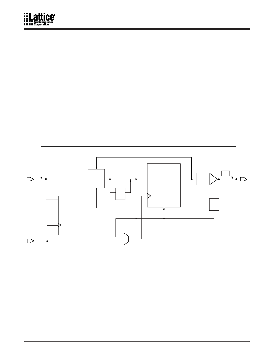
ispMACH 4A TIMING MODEL
The primary focus of the ispMACH 4A timing model is to accurately represent the timing in a
ispMACH 4A device, and at the same time, be easy to understand. This model accurately
describes all combinatorial and registered paths through the device, making a distinction
between internal feedback and external feedback. A signal uses internal feedback when it is fed
back into the switch matrix or block without having to go through the output buffer. The input
register specifications are also reported as internal feedback. When a signal is fed back into the
switch matrix after having gone through the output buffer, it is using external feedback.
The parameter, t
BUF
, is defined as the time it takes to go from feedback through the output buffer
to the I/O pad. If a signal goes to the internal feedback rather than to the I/O pad, the parameter
designator is followed by an "i". By adding t
BUF
to this internal parameter, the external parameter
is derived. For example, t
PD
= t
PDi
+ t
BUF
. A diagram representing the modularized ispMACH 4A
timing model is shown in Figure 15. Refer to the application note entitled MACH 4 Timing and
High Speed Design for a more detailed discussion about the timing parameters.
SPEEDLOCKING FOR GUARANTEED FIXED TIMING
The ispMACH 4A architecture allows allocation of up to 20 product terms to an individual
macrocell with the assistance of an XOR gate without incurring additional timing delays.
The design of the switch matrix and PAL blocks guarantee a fixed pin-to-pin delay that is
independent of the logic required by the design. Other competitive CPLDs incur serious timing
delays as product terms expand beyond their typical 4 or 5 product term limits. Speed and
SpeedLocking combine to give designs easy access to the performance required in today's
designs.
(External Feedback)
(Internal Feedback)
INPUT REG/
INPUT LATCH
t
SIRS
t
HIRS
t
SIL
t
HIL
t
SIRZ
t
HIRZ
t
SILZ
t
HILZ
t
PDILi
t
ICOSi
t
IGOSi
t
PDILZi
Q
t
SS(T)
t
SA(T)
t
H(S/A)
t
S(S/A)L
t
H(S/A)L
t
SRR
t
PDi
t
PDLi
t
CO(S/A)i
t
GO(S/A)i
t
SRi
COMB/DFF/TFF/
LATCH/SR*/JK*
S/R
IN
BLK CLK
OUT
t
PL
t
BUF
t
EA
t
ER
t
SLW
Q
Central
Switch
Matrix
*emulated
17466G-025
Figure 15. ispMACH 4A Timing Model

ispMACH 4A Family
21
IEEE 1149.1-COMPLIANT BOUNDARY SCAN TESTABILITY
All ispMACH 4A devices have boundary scan cells and are compliant to the IEEE 1149.1 standard.
This allows functional testing of the circuit board on which the device is mounted through a
serial scan path that can access all critical logic nodes. Internal registers are linked internally,
allowing test data to be shifted in and loaded directly onto test nodes, or test node data to be
captured and shifted out for verification. In addition, these devices can be linked into a board-
level serial scan path for more complete board-level testing.
IEEE 1149.1-COMPLIANT IN-SYSTEM PROGRAMMING
Programming devices in-system provides a number of significant benefits including: rapid
prototyping, lower inventory levels, higher quality, and the ability to make in-field modifications.
All ispMACH 4A devices provide In-System Programming (ISP) capability through their
Boundary ScanTest Access Ports. This capability has been implemented in a manner that ensures
that the port remains compliant to the IEEE 1149.1 standard. By using IEEE 1149.1 as the
communication interface through which ISP is achieved, customers get the benefit of a standard,
well-defined interface.
ispMACH 4A devices can be programmed across the commercial temperature and voltage range.
The PC-based LatticePRO software facilitates in-system programming of ispMACH 4A devices.
LatticePRO takes the JEDEC file output produced by the design implementation software, along
with information about the JTAG chain, and creates a set of vectors that are used to drive the
JTAG chain. LatticePRO software can use these vectors to drive a JTAG chain via the parallel port
of a PC. Alternatively, LatticePRO software can output files in formats understood by common
automated test equipment. This equpment can then be used to program ispMACH 4A devices
during the testing of a circuit board.
PCI COMPLIANT
ispMACH 4A devices in the -5/-55/-6/-65/-7/-10/-12 speed grades are compliant with the PCI
Local Bus Specification version 2.1, published by the PCI Special Interest Group (SIG). The 5-V
devices are fully PCI-compliant. The 3.3-V devices are mostly compliant but do not meet the PCI
condition to clamp the inputs as they rise above V
CC
because of their 5-V input tolerant feature.
SAFE FOR MIXED SUPPLY VOLTAGE SYSTEM DESIGNS
Both the 3.3-V and 5-V V
CC
ispMACH 4A devices are safe for mixed supply voltage system
designs. The 5-V devices will not overdrive 3.3-V devices above the output voltage of 3.3 V,
while they accept inputs from other 3.3-V devices. The 3.3-V device will accept inputs up to 5.5
V. Both the 5-V and 3.3-V versions have the same high-speed performance and provide easy-to-
use mixed-voltage design capability.
PULL UP OR BUS-FRIENDLY INPUTS AND I/Os
All ispMACH 4A devices have inputs and I/Os which feature the Bus-Friendly circuitry
incorporating two inverters in series which loop back to the input. This double inversion weakly
holds the input at its last driven logic state. While it is good design practice to tie unused pins
to a known state, the Bus-Friendly input structure pulls pins away from the input threshold
voltage where noise can cause high-frequency switching. At power-up, the Bus-Friendly latches
are reset to a logic level "1." For the circuit diagram, please refer to the document entitled MACH
Endurance Characteristics on the Lattice Data Book CD-ROM or Lattice web site.
22
ispMACH 4A Family
All ispMACH 4A devices have a programmable bit that configures all inputs and I/Os with either
pull-up or Bus-Friendly characteristics. If the device is configured in pull-up mode, all inputs
and I/O pins are weakly pulled up. For the circuit diagram, please refer to the document entitled
MACH Endurance Characteristics on the Lattice Data Book CD-ROM or Lattice web site.
POWER MANAGEMENT
Each individual PAL block in ispMACH 4A devices features a programmable low-power mode,
which results in power savings of up to 50%. The signal speed paths in the low-power PAL block
will be slower than those in the non-low-power PAL block. This feature allows speed critical
paths to run at maximum frequency while the rest of the signal paths operate in the low-power
mode.
PROGRAMMABLE SLEW RATE
Each ispMACH 4A device I/O has an individually programmable output slew rate control bit.
Each output can be individually configured for the higher speed transition (3 V/ns) or for the
lower noise transition (1 V/ns). For high-speed designs with long, unterminated traces, the slow-
slew rate will introduce fewer reflections, less noise, and keep ground bounce to a minimum.
For designs with short traces or well terminated lines, the fast slew rate can be used to achieve
the highest speed. The slew rate is adjusted independent of power.
POWER-UP RESET/SET
All flip-flops power up to a known state for predictable system initialization. If a macrocell is
configured to SET on a signal from the control generator, then that macrocell will be SET during
device power-up. If a macrocell is configured to RESET on a signal from the control generator
or is not configured for set/reset, then that macrocell will RESET on power-up. To guarantee
initialization values, the V
CC
rise must be monotonic, and the clock must be inactive until the
reset delay time has elapsed.
SECURITY BIT
A programmable security bit is provided on the ispMACH 4A devices as a deterrent to
unauthorized copying of the array configuration patterns. Once programmed, this bit defeats
readback of the programmed pattern by a device programmer, securing proprietary designs from
competitors. Programming and verification are also defeated by the security bit. The bit can only
be reset by erasing the entire device.
HOT SOCKETING
ispMACH 4A devices are well-suited for those applications that require hot socketing capability.
Hot socketing a device requires that the device, when powered down, can tolerate active signals
on the I/Os and inputs without being damaged. Additionally, it requires that the effects of the
powered-down MACH devices be minimal on active signals.
ispMACH 4A Family
23
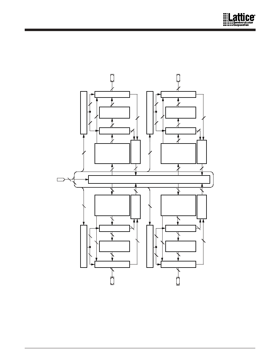
MACROCELL
M0
C0
M1
M2
M3
M4
M5
M6
M7
M8
M9
M10
M11
M12
M13
M14
M15
B
89
M0
M4A(3, 5)-64/32
M4A3-64/64
M4A(3, 5)-96/48
M4A(3, 5)-128/64
A
B
16
17
17
17
M4(3, 5)-192/96
M4(3, 5)-256/128
M4A3-384
M4A3-512
18
18
M1
M2
M3
M4
M5
M6
M7
M8
M9
M10
M11
M12
M13
M14
O0
O1
O2
O3
O4
O5
O6
O7
M15
CLK0
CLK1
CLK2
CLK3
I/O
CELL
I/O0
CLOCK
GENERATOR
MACROCELL
MACROCELL
MACROCELL
MACROCELL
MACROCELL
MACROCELL
CENTRAL
SWITCH MA
TRIX
MACROCELL
MACROCELL
MACROCELL
MACROCELL
MACROCELL
MACROCELL
MACROCELL
MACROCELL
MACROCELL
24
A
0
4
16
16
C1
C2
I/O
CELL
I/O1
C3
C4
I/O
CELL
I/O2
C5
C6
I/O
CELL
I/O3
C7
C8
I/O
CELL
I/O4
C9
C10
I/O
CELL
I/O5
C11
C12
I/O
CELL
I/O6
C13
C14
I/O
CELL
INPUT SWITCH
MATRIX
I/O7
C15
LOGIC ALLOCA
T
O
R
OUTPUT
SWITCH MA
TRIX
Figure 16. PAL Block for ispMACH 4A with 2:1 Macrocell - I/O Cell Ratio
24
ispMACH 4A Family
Figure 17. PAL Block for ispMACH 4A Devices with 1:1 Macrocell-I/O Cell Ratio (except M4A (3,5)-32/32)
MACROCELL
M0
C0
M1
M2
M3
M4
M5
M6
M7
M8
M9
M10
M11
M12
M13
M14
M15
B
97
M0
M1
M2
M3
M4
M5
M6
M7
M8
M9
M10
M11
M12
M13
M14
O0
O2
O4
O6
O8
O10
O12
O14
M15
I/O
CELL
I/O0
CLOCK
GENERATOR
MACROCELL
MACROCELL
MACROCELL
MACROCELL
MACROCELL
MACROCELL
CENTRAL SWITCH MA
TRIX
MACROCELL
MACROCELL
MACROCELL
MACROCELL
MACROCELL
MACROCELL
MACROCELL
MACROCELL
MACROCELL
O1
I/O
CELL
I/O1
32
A
0
4
16
16
C1
C2
I/O
CELL
I/O2
O3
I/O
CELL
I/O3
O5
I/O
CELL
I/O5
O7
I/O
CELL
I/O7
C3
C4
I/O
CELL
I/O4
C5
C6
I/O
CELL
I/O6
C7
C8
I/O
CELL
I/O8
O9
I/O
CELL
I/O9
O11
I/O
CELL
I/O11
C9
C10
I/O
CELL
I/O10
C11
C12
I/O
CELL
I/O12
O13
I/O
CELL
I/O13
O15
I/O
CELL
I/O15
C13
C14
I/O
CELL
INPUT
SWITCH
MATRIX
I/O14
C15
LOGIC ALLOCA
T
O
R
OUTPUT SWITCH MA
TRIX
CLK0
CLK1
CLK2
CLK3
M4A3-64/64
A
B
16
17
18
18
M4A3-256/160
M4A3-256/192
17466H-41

ispMACH 4A Family
25
17466H-042
MACROCELL
M0
C0
M1
M2
M3
M4
M5
M6
M7
M8
M9
M10
M11
M12
M13
M14
M15
17
97
M0
M1
M2
M3
M4
M5
M6
M7
M8
M9
M10
M11
M12
M13
M14
O0
O2
O4
O6
O8
O10
O12
O14
M15
I/O
CELL
I/O0
CLOCK
GENERATOR
MACROCELL
MACROCELL
MACROCELL
MACROCELL
MACROCELL
MACROCELL
CENTRAL SWITCH MA
TRIX
MACROCELL
MACROCELL
MACROCELL
MACROCELL
MACROCELL
MACROCELL
MACROCELL
MACROCELL
MACROCELL
O1
I/O
CELL
I/O1
32
16
0
2
16
16
C1
C2
I/O
CELL
I/O2
O3
I/O
CELL
I/O3
O5
I/O
CELL
I/O5
O7
I/O
CELL
I/O7
C3
C4
I/O
CELL
I/O4
C5
C6
I/O
CELL
I/O6
C7
C8
I/O
CELL
I/O8
O9
I/O
CELL
I/O9
O11
I/O
CELL
I/O11
C9
C10
I/O
CELL
I/O10
C11
C12
I/O
CELL
I/O12
O13
I/O
CELL
I/O13
O15
I/O
CELL
I/O15
C13
C14
I/O
CELL
INPUT
SWITCH
MATRIX
I/O14
C15
LOGIC ALLOCA
T
O
R
OUTPUT SWITCH MA
TRIX
OUTPUT SWITCH MA
TRIX
CLK0/I0
CLK0/I1
Figure 18. PAL Block for M4A (3,5)-32/32
26
ispMACH 4A Family
BLOCK DIAGRAM ≠ M4A(3,5)-32/32
17466H-019
Central Switch Matrix
2
2
CLK0/I0, CLK1/I1
I/O8≠I/O15
I/O0≠I/O7
I/O16≠I/O23
I/O24≠I/O31
I/O Cells
Output Switch
Matrix
Macrocells
8
8
16
8
8
8
33
4
4
4
4
8
8
I/O Cells
Output Switch
Matrix
Macrocells
66 X 98
AND Logic Array
and Logic Allocator
Clock Generator
Input Switch
Matrix
8
8
16
8
8
8
2
8
8
I/O Cells
Output Switch
Matrix
Macrocells
8
8
16
8
8
8
8
8
I/O Cells
Output Switch
Matrix
Macrocells
66 X 98
AND Logic Array
and Logic Allocator
8
8
16
8
8
8
2
8
8
Input Switch
Matrix
Input Switch
Matrix
Input Switch
Matrix
Clock Generator
OE
OE
OE
OE
Block A
Block B
33
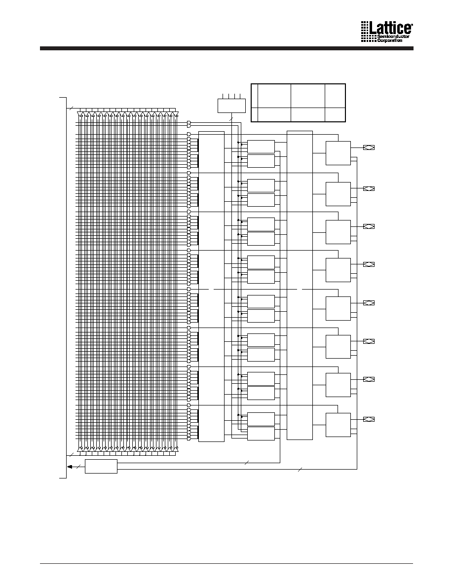
ispMACH 4A Family
27
BLOCK DIAGRAM ≠ M4A(3,5)-64/32
17466H-020
Central Switch Matrix
2
2
CLK0/I0, CLK1/I1
I/O0≠I/O7
I/O24≠I/O31
I/O16≠I/O23
I/O8≠I/O15
I/O Cells
Output Switch
Matrix
Macrocells
66 X 90
AND Logic Array
and Logic Allocator
Clock Generator
16
16
24
16
16
8
33
4
4
2
8
8
I/O Cells
Output Switch
Matrix
Macrocells
66 X 90
AND Logic Array
and Logic Allocator
Clock Generator
Input Switch
Matrix
16
16
24
16
16
8
33
4
4
2
8
8
I/O Cells
Output Switch
Matrix
Macrocells
66 X 90
AND Logic Array
and Logic Allocator
16
16
24
16
16
8
33
4
4
2
8
8
I/O Cells
Output Switch
Matrix
Macrocells
66 X 90
AND Logic Array
and Logic Allocator
16
16
24
16
16
8
33
4
4
2
8
8
Input Switch
Matrix
Input Switch
Matrix
Input Switch
Matrix
Clock Generator
Clock Generator
OE
OE
OE
OE
Block A
Block B
Block D
Block C

28
ispMACH 4A Family
BLOCK DIAGRAM ≠ M4A3-64/64
Central Switch Matrix
4
4
CLK0/I0, CLK1/I1
CLK2/I3, CLK3/I4
I/O Cells
Output Switch
Matrix
Macrocells
66 X 90
AND Logic Array
and Logic Allocator
Clock Generator
16
16
16
16
16
33
4
4
16
16
I/O Cells
Output Switch
Matrix
Macrocells
66 X 90
AND Logic Array
and Logic Allocator
Clock Generator
16
16
16
16
16
33
4
4
16
16
I/O Cells
Output Switch
Matrix
Macrocells
66 X 90
AND Logic Array
and Logic Allocator
16
16
16
16
16
33
4
4
16
16
I/O Cells
Output Switch
Matrix
Macrocells
66 X 90
AND Logic Array
and Logic Allocator
16
16
16
16
16
33
4
4
16
16
Clock Generator
Clock Generator
OE
OE
OE
OE
Block A
Block B
Block D
Block C
2
17466H-020A
ispMACH 4A Family
29
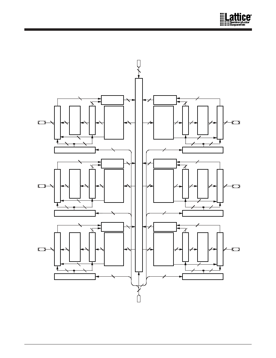
BLOCK DIAGRAM ≠ M4A(3,5)-96/48
4
4
4
CLK0/I0, CLK1/I1,
CLK2/I4, CLK3/I5
I2, I3, I6, I7
I/O16≠I/O23
I/O8≠I/O15
I/O0≠I/O7
I/O40≠I/O47
I/O32≠I/O39
I/O24≠I/O31
I/O Cells
Output Switch
Matrix
Macrocells
66 X 90
AND Logic Array
and Logic Allocator
Clock Generator
16
16
24
16
16
8
33
4
4
4
8
8
I/O Cells
Output Switch
Matrix
Macrocells
66 X 90
AND Logic Array
and Logic Allocator
Clock Generator
Input Switch
Matrix
16
16
24
16
16
8
33
4
4
4
8
8
I/O Cells
Output Switch
Matrix
Macrocells
66 X 90
AND Logic Array
and Logic Allocator
Clock Generator
Input Switch
Matrix
16
16
24
16
16
8
33
4
4
4
8
8
I/O Cells
Output Switch
Matrix
Macrocells
66 X 90
AND Logic Array
and Logic Allocator
16
16
24
16
16
8
33
4
4
4
8
8
I/O Cells
Output Switch
Matrix
Macrocells
66 X 90
AND Logic Array
and Logic Allocator
16
16
24
16
16
8
33
4
4
4
8
8
I/O Cells
Output Switch
Matrix
Macrocells
66 X 90
AND Logic Array
and Logic Allocator
16
16
24
16
16
8
33
4
4
4
8
8
OE
Input Switch
Matrix
Input Switch
Matrix
Input Switch
Matrix
Clock Generator
Clock Generator
Clock Generator
Input Switch
Matrix
OE
OE
OE
OE
OE
Block C
Block B
Block A
Block D
Block E
Block F
Central Switch Matrix
17466G-021

ispMACH 4A Family
30
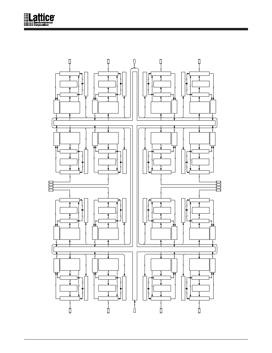
BLOCK DIAGRAM ≠ M4A(3,5)-128/64
Central Switch Matrix
4
4
2
CLK0/I0, CLK1/I1,
CLK2/I3, CLK3/I4
I2, I5
I/O0≠I/O7
I/O8≠I/O15
I/O16≠I/O23
I/O24≠I/031
I/O32≠I/O39
I/O40≠I/O47
I/O48≠I/O55
I/O56≠I/O63
I/O Cells
Output Switch
Matrix
Macrocells
66 X 90
AND Logic Array
and Logic Allocator
Clock Generator
16
16
24
16
16
8
33
4
4
4
8
8
I/O Cells
Output Switch
Matrix
Macrocells
66 X 90
AND Logic Array
and Logic Allocator
Clock Generator
Input Switch
Matrix
16
16
24
16
16
8
33
4
4
4
8
8
I/O Cells
Output Switch
Matrix
Macrocells
66 X 90
AND Logic Array
and Logic Allocator
Clock Generator
Input Switch
Matrix
16
16
24
16
16
8
33
4
4
4
8
8
I/O Cells
Output Switch
Matrix
Macrocells
66 X 90
AND Logic Array
and Logic Allocator
Clock Generator
Input Switch
Matrix
16
16
24
16
16
8
33
4
4
4
8
8
I/O Cells
Output Switch
Matrix
Macrocells
66 X 90
AND Logic Array
and Logic Allocator
16
16
24
16
16
8
33
4
4
4
8
8
I/O Cells
Output Switch
Matrix
Macrocells
66 X 90
AND Logic Array
and Logic Allocator
16
16
24
16
16
8
33
4
4
4
8
8
I/O Cells
Output Switch
Matrix
Macrocells
66 X 90
AND Logic Array
and Logic Allocator
16
16
24
16
16
8
33
4
4
4
8
8
I/O Cells
Output Switch
Matrix
Macrocells
66 X 90
AND Logic Array
and Logic Allocator
OE
16
16
24
16
16
8
33
4
4
4
8
8
Input Switch
Matrix
Input Switch
Matrix
Input Switch
Matrix
Clock Generator
Clock Generator
Clock Generator
Input Switch
Matrix
Input Switch
Matrix
Clock Generator
OE
OE
OE
OE
OE
OE
OE
Block A
Block B
Block C
Block D
Block H
Block G
Block F
Block E
17466H-022

ispMACH 4A Family
31
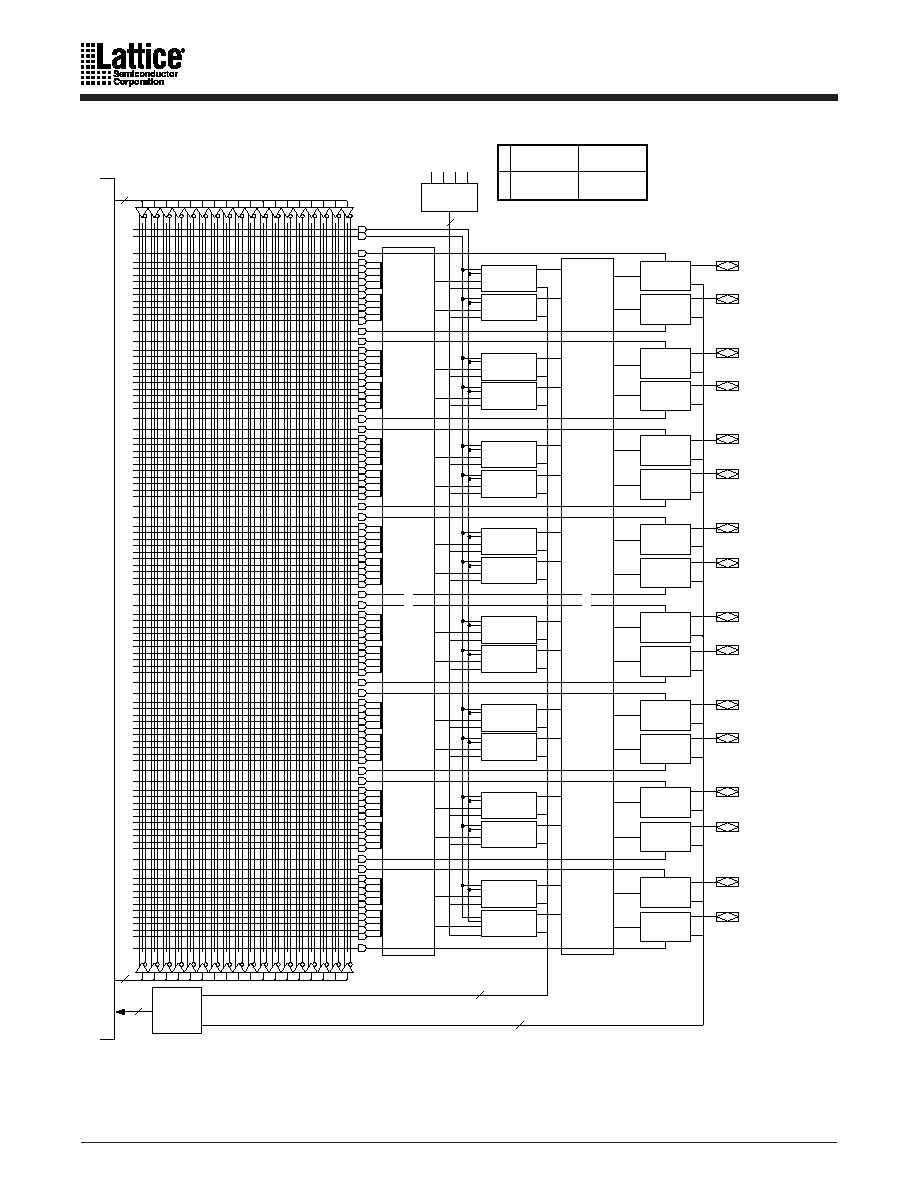
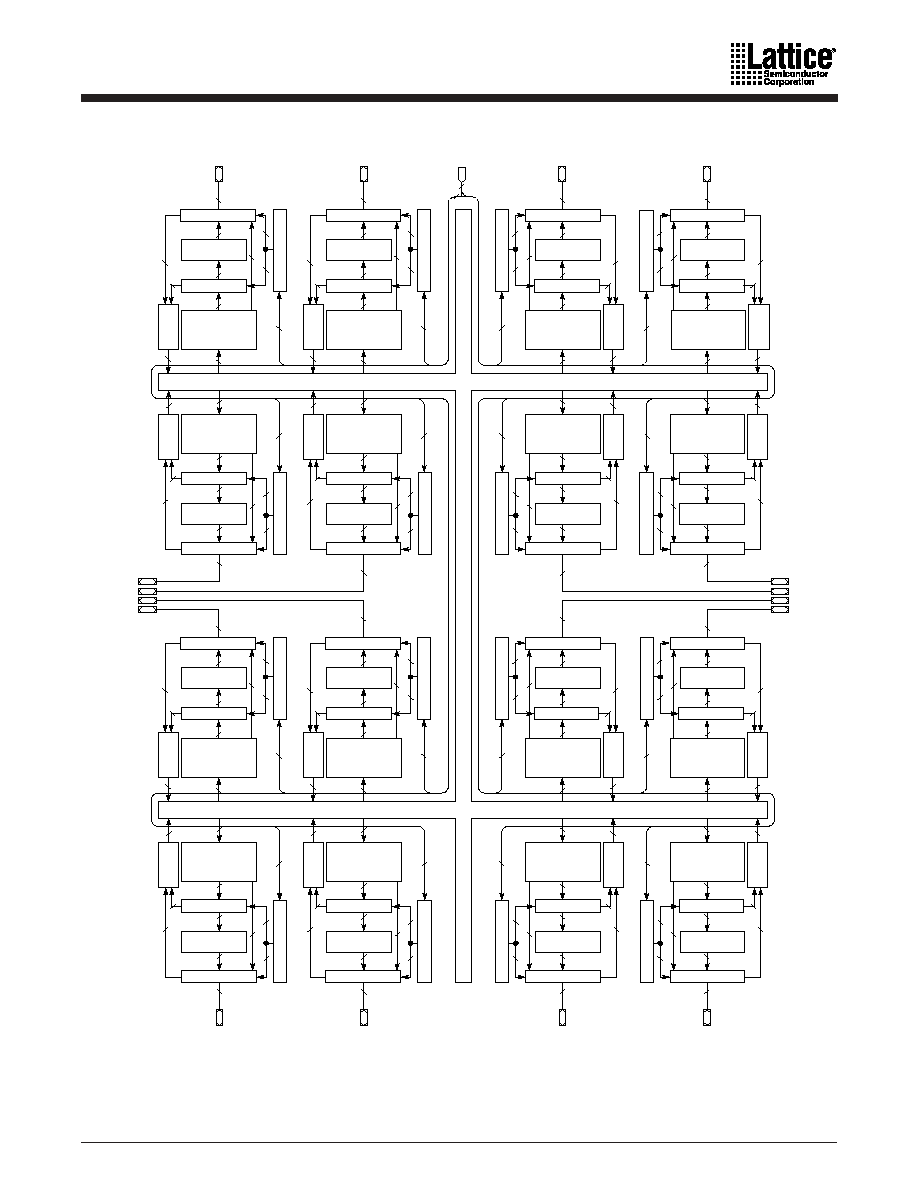
BLOCK DIAGRAM ≠ M4A(3,5)-192/96
Central Switch Matrix
Block B
I/O88--I/O95
CLK0--CLK3
I/O16--I/O23
Block E
I/O40--I/O47
Block H
I/O32--I/O39
Block G
I0--I15
I/O24--I/O31
Block F
Block A
I/O80--I/O87
Block K
I/O64--I/O71
Block L
I/O72--I/O79
Block C I/O8--I/O15
Block D I/O0--I/O7
I/O56--I/O63 Block J
I/O48--I/O55 Block I
I/O Cells
Macrocells
68 X 90
AND Logic Array
and Logic Allocator
Clock Generator
Input Switch
Matrix
Output Switch
Matrix
I/O Cells
Macrocells
68 X 90
AND Logic Array
and Logic Allocator
Clock Generator
Input Switch
Matrix
Output Switch
Matrix
I/O Cells
Macrocells
68 X 90
AND Logic Array
and Logic Allocator
Clock Generator
Input Switch
Matrix
Output Switch
Matrix
I/O Cells
Macrocells
68 X 90
AND Logic Array
and Logic Allocator
Clock Generator
Input Switch
Matrix
Output Switch
Matrix
I/O Cells
Macrocells
68 X 90
AND Logic Array
and Logic Allocator
Clock Generator
Input Switch
Matrix
Output Switch
Matrix
I/O Cells
Macrocells
68 X 90
AND Logic Array
and Logic Allocator
Clock Generator
Input Switch
Matrix
Output Switch
Matrix
I/O Cells
Macrocells
68 X 90
AND Logic Array
and Logic Allocator
Clock Generator
Input Switch
Matrix
Output Switch
Matrix
I/O Cells
Macrocells
68 X 90
AND Logic Array
and Logic Allocator
Clock Generator
Input Switch
Matrix
Output Switch
Matrix
I/O Cells
Macrocells
68 X 90
AND Logic Array
and Logic Allocator
Clock Generator
Input Switch
Matrix
Output Switch
Matrix
I/O Cells
Macrocells
68 X 90
AND Logic Array
and Logic Allocator
Clock Generator
Input Switch
Matrix
Output Switch
Matrix
I/O Cells
Macrocells
68 X 90
AND Logic Array
and Logic Allocator
Clock Generator
Input Switch
Matrix
Output Switch
Matrix
I/O Cells
Macrocells
68 X 90
AND Logic Array
and Logic Allocator
Clock Generator
Input Switch
Matrix
Output Switch
Matrix
16
4
4
OE
8
16
8
4
16
24
8
16
16
34
4
4
8
24
34
4
8
8
16
16
4
4
16
16
OE
8
24
34
4
8
8
16
16
4
4
16
16
OE
8
16
8
4
16
24
8
16
16
34
34
34
34
34
34
34
34
34
4
4
OE
OE
8
16
8
4
16
24
8
16
16
4
4
8
24
4
8
8
16
16
4
4
16
16
OE
8
24
4
8
8
16
16
4
4
16
16
OE
OE
4
4
8
24
16
16
8
16
8
4
16
OE
4
4
24
16
16
8
16
16
4
8
8
OE
4
4
24
16
16
8
16
16
4
8
8
4
4
8
24
16
16
8
16
8
4
16
OE
8
16
8
4
16
24
8
16
16
4
4
OE
17466G-067
32
ispMACH 4A Family
BLOCK DIAGRAM ≠ M4A(3,5)-256/128
Central Switch Matrix
Block B
I/O8≠I/O15
CLK0≠CLK3
I/O48≠I/O55
Block G
I/O72≠I/O79
Block J
I/O64≠I/O71
Block I
I0≠I13
I/O56≠I/O63
Block H
Block A
I/O0≠I/O7
Block O
I/O112≠I/O119
Block P
I/O120≠I/O127
Block C I/O16≠I/O23
Block D I/O24≠I/O31
Block E I/O32≠I/O39
Block F I/O40≠I/O47
I/O104≠I/O111 Block N
I/O96≠I/O103 Block M
I/O88≠I/O95 Block L
I/O80≠I/O87 Block K
I/O Cells
Macrocells
68 X 90
AND Logic Array
and Logic Allocator
Clock Generator
Input Switch
Matrix
Output Switch
Matrix
I/O Cells
Macrocells
68 X 90
AND Logic Array
and Logic Allocator
Clock Generator
Input Switch
Matrix
Output Switch
Matrix
I/O Cells
Macrocells
68 X 90
AND Logic Array
and Logic Allocator
Clock Generator
Input Switch
Matrix
Output Switch
Matrix
I/O Cells
Macrocells
68 X 90
AND Logic Array
and Logic Allocator
Clock Generator
Input Switch
Matrix
Output Switch
Matrix
I/O Cells
Macrocells
68 X 90
AND Logic Array
and Logic Allocator
Clock Generator
Input Switch
Matrix
Output Switch
Matrix
I/O Cells
Macrocells
68 X 90
AND Logic Array
and Logic Allocator
Clock Generator
Input Switch
Matrix
Output Switch
Matrix
I/O Cells
Macrocells
68 X 90
AND Logic Array
and Logic Allocator
Clock Generator
Input Switch
Matrix
Output Switch
Matrix
I/O Cells
Macrocells
68 X 90
AND Logic Array
and Logic Allocator
Clock Generator
Input Switch
Matrix
Output Switch
Matrix
I/O Cells
Macrocells
68 X 90
AND Logic Array
and Logic Allocator
Clock Generator
Input Switch
Matrix
Output Switch
Matrix
I/O Cells
Macrocells
68 X 90
AND Logic Array
and Logic Allocator
Clock Generator
Input Switch
Matrix
Output Switch
Matrix
I/O Cells
Macrocells
68 X 90
AND Logic Array
and Logic Allocator
Clock Generator
Input Switch
Matrix
Output Switch
Matrix
I/O Cells
Macrocells
68 X 90
AND Logic Array
and Logic Allocator
Clock Generator
Input Switch
Matrix
Output Switch
Matrix
I/O Cells
Macrocells
68 X 90
AND Logic Array
and Logic Allocator
Clock Generator
Input Switch
Matrix
Output Switch
Matrix
I/O Cells
Macrocells
68 X 90
AND Logic Array
and Logic Allocator
Clock Generator
Input Switch
Matrix
Output Switch
Matrix
I/O Cells
Macrocells
68 X 90
AND Logic Array
and Logic Allocator
Clock Generator
Input Switch
Matrix
Output Switch
Matrix
I/O Cells
Macrocells
68 X 90
AND Logic Array
and Logic Allocator
Clock Generator
Input Switch
Matrix
Output Switch
Matrix
14
4
4
OE
8
16
8
4
16
24
8
16
16
34
4
4
8
24
34
4
8
8
16
16
4
4
16
16
OE
8
24
34
4
8
8
16
16
4
4
16
16
OE
OE
4
4
8
34
24
16
16
8
16
8
4
16
OE
4
4
34
24
16
16
8
16
16
4
8
8
OE
4
4
34
24
16
16
8
16
16
4
8
8
4
4
8
34
24
16
16
8
16
8
4
16
OE
8
16
8
4
16
24
8
16
16
34
4
4
OE
OE
8
16
8
4
16
24
8
16
16
34
4
4
8
24
34
4
8
8
16
16
4
4
16
16
OE
8
24
34
4
8
8
16
16
4
4
16
16
OE
OE
4
4
8
34
24
16
16
8
16
8
4
16
OE
4
4
34
24
16
16
8
16
16
4
8
8
OE
4
4
34
24
16
16
8
16
16
4
8
8
4
4
8
34
24
16
16
8
16
8
4
16
OE
8
16
8
4
16
24
8
16
16
34
4
4
OE
17466G-024
ispMACH 4A Family
33
BLOCK DIAGRAM ≠ M4A3-256/160, M4A3-256/192
Central Switch Matrix
Block B
CLK0≠CLK3
Block G
Block J
Block I
Block H
Block A
Block O
Block P
Block C
Block D
Block E
Block F
Block N
Block M
Block L
Block K
I/O Cells
Macrocells
72 X 98
AND Logic Array
and Logic Allocator
Clock Generator
Input Switch
Matrix
Output Switch
Matrix
I/O Cells
Macrocells
72 X 98
AND Logic Array
and Logic Allocator
Clock Generator
Input Switch
Matrix
Output Switch
Matrix
I/O Cells
Macrocells
72 X 98
AND Logic Array
and Logic Allocator
Clock Generator
Input Switch
Matrix
Output Switch
Matrix
I/O Cells
Macrocells
72 X 98
AND Logic Array
and Logic Allocator
Clock Generator
Input Switch
Matrix
Output Switch
Matrix
I/O Cells
Macrocells
72 X 98
AND Logic Array
and Logic Allocator
Clock Generator
Input Switch
Matrix
Output Switch
Matrix
I/O Cells
Macrocells
72 X 98
AND Logic Array
and Logic Allocator
Clock Generator
Input Switch
Matrix
Output Switch
Matrix
I/O Cells
Macrocells
72 X 98
AND Logic Array
and Logic Allocator
Clock Generator
Input Switch
Matrix
Output Switch
Matrix
I/O Cells
Macrocells
72 X 98
AND Logic Array
and Logic Allocator
Clock Generator
Input Switch
Matrix
Output Switch
Matrix
I/O Cells
Macrocells
72 X 98
AND Logic Array
and Logic Allocator
Clock Generator
Input Switch
Matrix
Output Switch
Matrix
I/O Cells
Macrocells
72 X 98
AND Logic Array
and Logic Allocator
Clock Generator
Input Switch
Matrix
Output Switch
Matrix
I/O Cells
Macrocells
72 X 98
AND Logic Array
and Logic Allocator
Clock Generator
Input Switch
Matrix
Output Switch
Matrix
I/O Cells
Macrocells
72 X 98
AND Logic Array
and Logic Allocator
Clock Generator
Input Switch
Matrix
Output Switch
Matrix
I/O Cells
Macrocells
72 X 98
AND Logic Array
and Logic Allocator
Clock Generator
Input Switch
Matrix
Output Switch
Matrix
I/O Cells
Macrocells
72 X 98
AND Logic Array
and Logic Allocator
Clock Generator
Input Switch
Matrix
Output Switch
Matrix
I/O Cells
Macrocells
72 X 98
AND Logic Array
and Logic Allocator
Clock Generator
Input Switch
Matrix
Output Switch
Matrix
I/O Cells
Macrocells
72 X 98
AND Logic Array
and Logic Allocator
Clock Generator
Input Switch
Matrix
Output Switch
Matrix
4
4
OE
16
16
16
4
16
32
16
16
16
36
4
4
16
32
36
4
16
16
16
16
4
4
16
16
OE
16
32
36
4
16
16
16
16
4
4
16
16
OE
OE
4
4
16
36
32
16
16
16
16
16
4
16
OE
4
4
36
32
16
16
16
16
16
4
16
16
OE
4
4
36
32
16
16
16
16
16
4
16
16
4
4
16
36
32
16
16
16
16
16
4
16
OE
16
16
16
4
16
32
16
16
16
36
4
4
OE
OE
16
16
16
4
16
32
16
16
16
36
4
4
16
32
36
4
16
16
16
16
4
4
16
16
OE
16
32
36
4
16
16
16
16
4
4
16
16
OE
OE
4
4
16
36
32
16
16
16
16
16
4
16
OE
4
4
36
32
16
16
16
16
16
4
16
16
OE
4
4
36
32
16
16
16
16
16
4
16
16
4
4
16
36
32
16
16
16
16
16
4
16
OE
16
16
16
4
16
32
16
16
16
36
4
4
OE
17466G-050

34
ispMACH 4A Family
BLOCK DIAGRAM ≠ M4A3-384/160, M4A3-384/192
Central Switch Matrix
Block B
CLK0≠CLK3
Block A
Block GX
Block HX
Block C
Block F
Block D
Block E
Block FX
Block CX
Block EX
Block DX
I/O Cells
Macrocells
72 X 90
AND Logic Array
and Logic Allocator
Clock Generator
Input Switch
Matrix
Output Switch
Matrix
I/O Cells
Macrocells
72 X 90
AND Logic Array
and Logic Allocator
Clock Generator
Input Switch
Matrix
Output Switch
Matrix
I/O Cells
Macrocells
72 X 90
AND Logic Array
and Logic Allocator
Clock Generator
Input Switch
Matrix
Output Switch
Matrix
I/O Cells
Macrocells
72 X 90
AND Logic Array
and Logic Allocator
Clock Generator
Input Switch
Matrix
Output Switch
Matrix
I/O Cells
Macrocells
72 X 90
AND Logic Array
and Logic Allocator
Clock Generator
Input Switch
Matrix
Output Switch
Matrix
I/O Cells
Macrocells
72 X 90
AND Logic Array
and Logic Allocator
Clock Generator
Input Switch
Matrix
Output Switch
Matrix
I/O Cells
Macrocells
72 X 90
AND Logic Array
and Logic Allocator
Clock Generator
Input Switch
Matrix
Output Switch
Matrix
I/O Cells
Macrocells
72 X 90
AND Logic Array
and Logic Allocator
Clock Generator
Input Switch
Matrix
Output Switch
Matrix
4
4
4
OE
8
16
8
4
16
24
8
16
16
36
4
4
8
24
36
4
8
8
16
16
4
4
16
16
OE
8
24
36
4
8
8
16
16
4
4
16
16
OE
OE
4
4
8
36
24
16
16
8
16
8
4
16
OE
4
4
36
24
16
16
8
16
16
4
8
8
OE
4
4
36
24
16
16
8
16
16
4
8
8
4
4
8
36
24
16
16
8
16
8
4
16
OE
8
16
8
4
16
24
8
16
16
36
4
4
OE
I/O Cells
Macrocells
72 X 90
AND Logic Array
and Logic Allocator
Clock Generator
Input Switch
Matrix
Output Switch
Matrix
I/O Cells
Macrocells
72 X 90
AND Logic Array
and Logic Allocator
Clock Generator
Input Switch
Matrix
Output Switch
Matrix
I/O Cells
Macrocells
72 X 90
AND Logic Array
and Logic Allocator
Clock Generator
Input Switch
Matrix
Output Switch
Matrix
I/O Cells
Macrocells
72 X 90
AND Logic Array
and Logic Allocator
Clock Generator
Input Switch
Matrix
Output Switch
Matrix
I/O Cells
Macrocells
72 X 90
AND Logic Array
and Logic Allocator
Clock Generator
Input Switch
Matrix
Output Switch
Matrix
I/O Cells
Macrocells
72 X 90
AND Logic Array
and Logic Allocator
Clock Generator
Input Switch
Matrix
Output Switch
Matrix
I/O Cells
Macrocells
72 X 90
AND Logic Array
and Logic Allocator
Clock Generator
Input Switch
Matrix
Output Switch
Matrix
I/O Cells
Macrocells
72 X 90
AND Logic Array
and Logic Allocator
Clock Generator
Input Switch
Matrix
Output Switch
Matrix
OE
8
16
8
4
16
24
8
16
16
36
4
4
8
24
36
4
8
8
16
16
4
4
16
16
OE
8
24
36
4
8
8
16
16
4
4
16
16
OE
OE
4
4
8
36
24
16
16
8
16
8
4
16
OE
4
4
36
24
16
16
8
16
16
4
8
8
OE
4
4
36
24
16
16
8
16
16
4
8
8
4
4
8
36
24
16
16
8
16
8
4
16
OE
8
16
8
4
16
24
8
16
16
36
4
4
OE
Block G
Block J
Block H
Block I
Block BX
Block O
Block AX
Block P
Detail A
Repeat Detail A
Block L
Block K
Block M
Block N
17466G-067
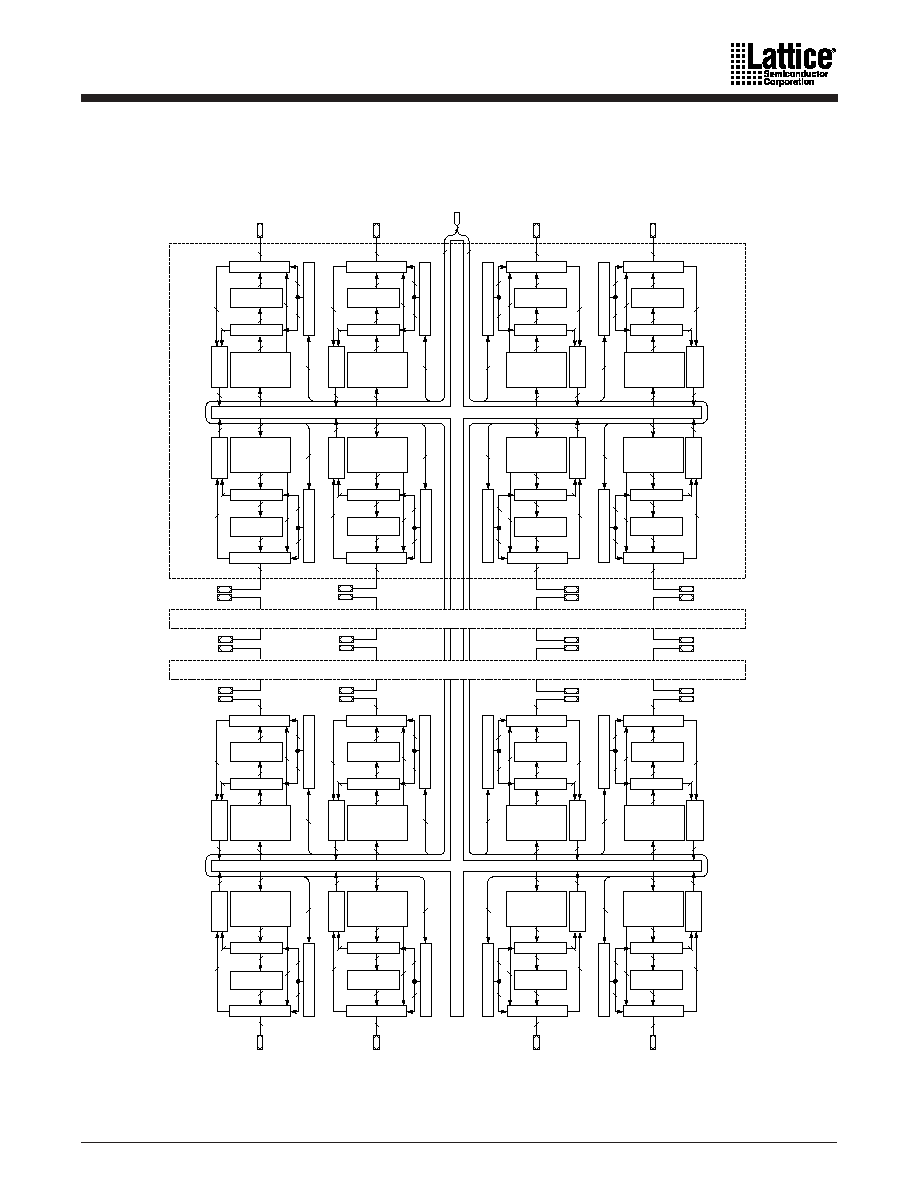
ispMACH 4A Family
35
BLOCK DIAGRAM - M4A3-512/160, M4A3-512/192, M4A3-512/256
Central Switch Matrix
Block B
CLK0≠CLK3
Block A
Block OX
Block PX
Block C
Block F
Block D
Block E
Block NX
Block KX
Block MX
Block LX
I/O Cells
Macrocells
72 X 90
AND Logic Array
and Logic Allocator
Clock Generator
Input Switch
Matrix
Output Switch
Matrix
I/O Cells
Macrocells
72 X 90
AND Logic Array
and Logic Allocator
Clock Generator
Input Switch
Matrix
Output Switch
Matrix
I/O Cells
Macrocells
72 X 90
AND Logic Array
and Logic Allocator
Clock Generator
Input Switch
Matrix
Output Switch
Matrix
I/O Cells
Macrocells
72 X 90
AND Logic Array
and Logic Allocator
Clock Generator
Input Switch
Matrix
Output Switch
Matrix
I/O Cells
Macrocells
72 X 90
AND Logic Array
and Logic Allocator
Clock Generator
Input Switch
Matrix
Output Switch
Matrix
I/O Cells
Macrocells
72 X 90
AND Logic Array
and Logic Allocator
Clock Generator
Input Switch
Matrix
Output Switch
Matrix
I/O Cells
Macrocells
72 X 90
AND Logic Array
and Logic Allocator
Clock Generator
Input Switch
Matrix
Output Switch
Matrix
I/O Cells
Macrocells
72 X 90
AND Logic Array
and Logic Allocator
Clock Generator
Input Switch
Matrix
Output Switch
Matrix
OE
8
16
8
4
16
24
8
16
16
36
4
4
8
24
36
4
8
8
16
16
4
4
16
16
OE
8
24
36
4
8
8
16
16
4
4
16
16
OE
OE
4
4
8
36
24
16
16
8
16
8
4
16
OE
4
4
36
24
16
16
8
16
16
4
8
8
OE
4
4
36
24
16
16
8
16
16
4
8
8
4
4
8
36
24
16
16
8
16
8
4
16
OE
8
16
8
4
16
24
8
16
16
36
4
4
OE
I/O Cells
Macrocells
72 X 90
AND Logic Array
and Logic Allocator
Clock Generator
Input Switch
Matrix
Output Switch
Matrix
I/O Cells
Macrocells
72 X 90
AND Logic Array
and Logic Allocator
Clock Generator
Input Switch
Matrix
Output Switch
Matrix
I/O Cells
Macrocells
72 X 90
AND Logic Array
and Logic Allocator
Clock Generator
Input Switch
Matrix
Output Switch
Matrix
I/O Cells
Macrocells
72 X 90
AND Logic Array
and Logic Allocator
Clock Generator
Input Switch
Matrix
Output Switch
Matrix
I/O Cells
Macrocells
72 X 90
AND Logic Array
and Logic Allocator
Clock Generator
Input Switch
Matrix
Output Switch
Matrix
I/O Cells
Macrocells
72 X 90
AND Logic Array
and Logic Allocator
Clock Generator
Input Switch
Matrix
Output Switch
Matrix
I/O Cells
Macrocells
72 X 90
AND Logic Array
and Logic Allocator
Clock Generator
Input Switch
Matrix
Output Switch
Matrix
I/O Cells
Macrocells
72 X 90
AND Logic Array
and Logic Allocator
Clock Generator
Input Switch
Matrix
Output Switch
Matrix
OE
8
16
8
4
16
24
8
16
16
36
4
4
8
24
36
4
8
8
16
16
4
4
16
16
OE
8
24
36
4
8
8
16
16
4
4
16
16
OE
OE
4
4
8
36
24
16
16
8
16
8
4
16
OE
4
4
36
24
16
16
8
16
16
4
8
8
OE
4
4
36
24
16
16
8
16
16
4
8
8
4
4
8
36
24
16
16
8
16
8
4
16
OE
8
16
8
4
16
24
8
16
16
36
4
4
OE
Block G
Block J
Block H
Block I
Block JX
Block GX
Block IX
Block HX
Block K
Block N
Block L
Block M
Block FX
Block CX
Block EX
Block DX
Detail A
Repeat Detail A
Repeat Detail A
Block P
Block O
Block AX
Block BX
4
4
4
17466G-068

36
ispMACH 4A Family
ABSOLUTE MAXIMUM RATINGS
M4A5
Storage Temperature . . . . . . . . . . . . . . . -65
∞C to +150∞C
Ambient Temperature
with Power Applied . . . . . . . . . . . . . . . .-55
∞C to +100∞C
Device Junction Temperature . . . . . . . . . . . . . . . +130
∞C
Supply Voltage
with Respect to Ground . . . . . . . . . . . . . -0.5 V to +7.0 V
DC Input Voltage . . . . . . . . . . . . . . . -0.5 V to V
CC
+ 0.5 V
Static Discharge Voltage . . . . . . . . . . . . . . . . . . . . 2000 V
Latchup Current (T
A
= -40
∞C to +85∞C) . . . . . . . 200 mA
Stresses above those listed under Absolute Maximum
Ratings may cause permanent device failure. Functionality
at or above these limits is not implied. Exposure to Absolute
Maximum Ratings for extended periods may affect device
reliability.
OPERATING RANGES
Commercial (C) Devices
Ambient Temperature (T
A
)
Operating in Free Air . . . . . . . . . . . . . . . . . 0
∞C to +70∞C
Supply Voltage (V
CC
)
with Respect to Ground . . . . . . . . . . +4.75 V to +5.25 V
Industrial (I) Devices
Ambient Temperature (T
A
)
Operating in Free Air . . . . . . . . . . . . . . . . -40
∞C to +85∞C
Supply Voltage (V
CC
)
with Respect to Ground . . . . . . . . . . . +4.50 V to +5.5 V
Operating ranges define those limits between which the func-
tionality of the device is guaranteed.
Notes:
1. Total I
OL
for one PAL block should not exceed 64 mA.
2. These are absolute values with respect to device ground, and all overshoots due to system or tester noise are included.
3. I/O pin leakage is the worst case of I
IL
and I
OZL
(or I
IH
and I
OZH
).
4. Not more than one output should be shorted at a time and duration of the short-circuit should not exceed one second.
V
OUT
= 0.5 V has been chosen to avoid test problems caused by tester ground degradation.
5-V DC CHARACTERISTICS OVER OPERATING RANGES
Parameter
Symbol
Parameter Description
Test Conditions
Min
Typ
Max
Unit
V
OH
Output HIGH Voltage
I
OH
= ≠3.2 mA, V
CC
= Min, V
IN
= V
IH
or V
IL
2.4
V
I
OH
= -100 µA, V
CC
= Max, V
IN
= V
IH
or V
IL
3.3
3.6
V
V
OL
Output LOW Voltage
I
OL
= 24 mA, V
CC
= Min, V
IN
= V
IH
or V
IL
(Note 1)
0.5
V
V
IH
Input HIGH Voltage
Guaranteed Input Logical HIGH Voltage for all Inputs
(Note 2)
2.0
V
V
IL
Input LOW Voltage
Guaranteed Input Logical LOW Voltage for all Inputs
(Note 2)
0.8
V
I
IH
Input HIGH Leakage Current
V
IN
= 5.25 V, V
CC
= Max (Note 3)
10
µA
I
IL
Input LOW Leakage Current
V
IN
= 0 V, V
CC
= Max (Note 3)
≠10
µA
I
OZH
Off-State Output Leakage Current HIGH
V
OUT
= 5.25 V, V
CC
= Max, V
IN
= V
IH
or V
IL
(Note 3)
10
µA
I
OZL
Off-State Output Leakage Current LOW
V
OUT
= 0 V, V
CC
= Max , V
IN
= V
IH
or V
IL
(Note 3)
≠10
µA
I
SC
Output Short-Circuit Current
V
OUT
= 0.5 V, V
CC
= Max (Note 4)
≠30
≠160
mA
ispMACH 4A Family
37
ABSOLUTE MAXIMUM RATINGS
M4A3
Storage Temperature . . . . . . . . . . . . . . . -65
∞C to +150∞C
Ambient Temperature
with Power Applied . . . . . . . . . . . . . . . .-55
∞C to +100∞C
Device Junction Temperature . . . . . . . . . . . . . . . +130
∞C
Supply Voltage
with Respect to Ground . . . . . . . . . . . . . -0.5 V to +4.5 V
DC Input Voltage . . . . . . . . . . . . . . . . . . . . -0.5 V to 6.0 V
Static Discharge Voltage . . . . . . . . . . . . . . . . . . . . 2000 V
Latchup Current (T
A
= -40
∞C to +85∞C) . . . . . . . 200 mA
Stresses above those listed under Absolute Maximum
Ratings may cause permanent device failure. Functionality
at or above these limits is not implied. Exposure to Absolute
Maximum Ratings for extended periods may affect device
reliability.
OPERATING RANGES
Commercial (C) Devices
Ambient Temperature (T
A
)
Operating in Free Air . . . . . . . . . . . . . . . . . 0
∞C to +70∞C
Supply Voltage (V
CC
)
with Respect to Ground . . . . . . . . . . . . +3.0 V to +3.6 V
Industrial (I) Devices
Ambient Temperature (T
A
)
Operating in Free Air . . . . . . . . . . . . . . . . -40
∞C to +85∞C
Supply Voltage (V
CC
)
with Respect to Ground . . . . . . . . . . . . +3.0 V to +3.6 V
Operating ranges define those limits between which the func-
tionality of the device is guaranteed.
Notes:
1. Total I
OL
for one PAL block should not exceed 64 mA.
2. I/O pin leakage is the worst case of I
IL
and I
OZL
(or I
IH
and I
OZH
).
3. Not more than one output should be shorted at a time and duration of the short-circuit should not exceed one second.
Notes:
1. See "MACH Switching Test Circuit" document on the Literature Download page of the Lattice web site.
2. This parameter does not apply to flip-flops in the emulated mode since the feedback path is required for emulation.
3.3-V DC CHARACTERISTICS OVER OPERATING RANGES
Parameter
Symbol
Parameter Description
Test Conditions
Min
Typ
Max
Unit
V
OH
Output HIGH Voltage
V
CC
= Min
V
IN
= V
IH
or V
IL
I
OH
= ≠100 µA
V
CC
≠ 0.2
V
I
OH
= ≠3.2 mA
2.4
V
V
OL
Output LOW Voltage
V
CC
= Min
V
IN
= V
IH
or V
IL
(Note 1)
I
OL
= 100 µA
0.2
V
I
OL
= 24 mA
0.5
V
V
IH
Input HIGH Voltage
Guaranteed Input Logical HIGH Voltage for all
Inputs
2.0
5.5
V
V
IL
Input LOW Voltage
Guaranteed Input Logical LOW Voltage for all
Inputs
≠0.3
0.8
V
I
IH
Input HIGH Leakage Current
V
IN
= 3.6 V, V
CC
= Max (Note 2)
5
µA
I
IL
Input LOW Leakage Current
V
IN
= 0 V, V
CC
= Max (Note 2)
≠5
µA
I
OZH
Off-State Output Leakage Current HIGH
V
OUT
= 3.6 V, V
CC
= Max
V
IN
= V
IH
or V
IL
(Note 2)
5
µA
I
OZL
Off-State Output Leakage Current LOW
V
OUT
= 0 V, V
CC
= Max
V
IN
= V
IH
or V
IL
(Note 2)
≠5
µA
I
SC
Output Short-Circuit Current
V
OUT
= 0.5 V, V
CC
= Max (Note 3)
≠15
≠160
mA
38
ispMACH 4A Family
ispMACH 4A TIMING PARAMETERS OVER OPERATING RANGES
1
-5
-55
-6
-65
-7
-10
-12
-14
Unit
Min Max Min Max Min Max Min Max Min Max Min Max Min Max Min Max
Combinatorial Delay:
t
PDi
Internal combinatorial propagation
delay
3.5
4.0
4.3
4.5
5.0
7.0
9.0
11.0
ns
t
PD
Combinatorial propagation delay
5.0
5.5
6.0
6.5
7.5
10.0
12.0
14.0
ns
Registered Delays:
t
SS
Synchronous clock setup time, D-type
register
3.0
3.5
3.5
3.5
5.0
5.5
7.0
10.0
ns
t
SST
Synchronous clock setup time, T-type
register
4.0
4.0
4.0
4.0
6.0
6.5
8.0
11.0
ns
t
SA
Asynchronous clock setup time, D-type
register
2.5
2.5
2.5
3.0
3.5
4.0
5.0
8.0
ns
t
SAT
Asynchronous clock setup time, T-type
register
3.0
3.0
3.0
3.5
4.5
5.0
6.0
9.0
ns
t
HS
Synchronous clock hold time
0.0
0.0
0.0
0.0
0.0
0.0
0.0
0.0
ns
t
HA
Asynchronous clock hold time
2.5
2.5
2.5
3.0
3.5
4.0
5.0
8.0
ns
t
COSi
Synchronous clock to internal output
2.5
2.5
2.8
3.0
3.0
3.0
3.5
3.5
ns
t
COS
Synchronous clock to output
4.0
4.0
4.5
5.0
5.5
6.0
6.5
6.5
ns
t
COAi
Asynchronous clock to internal output
5.0
5.0
5.0
5.0
6.0
8.0
10.0
12.0
ns
t
COA
Asynchronous clock to output
6.5
6.5
6.8
7.0
8.5
11.0
13.0
15.0
ns
Latched Delays:
t
SSL
Synchronous latch setup time
4.0
4.0
4.0
4.5
6.0
7.0
8.0
10.0
ns
t
SAL
Asynchronous latch setup time
3.0
3.0
3.5
3.5
4.0
4.0
5.0
8.0
ns
t
HSL
Synchronous latch hold time
0.0
0.0
0.0
0.0
0.0
0.0
0.0
0.0
ns
t
HAL
Asynchronous latch hold time
3.0
3.0
3.5
3.5
4.0
4.0
5.0
8.0
ns
t
PDLi
Transparent latch to internal output
5.5
5.5
5.8
6.0
7.5
9.0
11.0
12.0
ns
t
PDL
Propagation delay through transparent
latch to output
7.0
7.0
7.5
8.0
10.0
12.0
14.0
15.0
ns
t
GOSi
Synchronous gate to internal output
3.0
3.0
3.0
3.0
3.5
4.5
7.0
8.0
ns
t
GOS
Synchronous gate to output
4.5
4.5
4.8
5.0
6.0
7.5
10.0
11.0
ns
t
GOAi
Asynchronous gate to internal output
6.0
6.0
6.0
6.0
8.5
10.0
13.0
15.0
ns
t
GOA
Asynchronous gate to output
7.5
7.5
7.8
8.0
11.0
13.0
16.0
18.0
ns
Input Register Delays:
t
SIRS
Input register setup time
1.5
1.5
2.0
2.0
2.0
2.0
2.0
2.0
ns
t
HIRS
Input register hold time
2.5
2.5
3.0
3.0
3.0
3.0
3.0
4.0
ns
t
ICOSi
Input register clock to internal feedback
3.0
3.0
3.0
3.0
3.5
4.5
6.0
6.0
ns
Input Latch Delays:
t
SIL
Input latch setup time
1.5
1.5
1.5
2.0
2.0
2.0
2.0
2.0
ns
t
HIL
Input latch hold time
2.5
2.5
2.5
3.0
3.0
3.0
3.0
4.0
ns
t
IGOSi
Input latch gate to internal feedback
3.5
3.5
3.8
4.0
4.0
4.0
4.0
5.0
ns
t
PDILi
Transparent input latch to internal
feedback
1.5
1.5
1.5
1.5
2.0
2.0
2.0
2.0
ns
ispMACH 4A Family
39
Input Register Delays with ZHT Option:
t
SIRZ
Input register setup time - ZHT
6.0
6.0
6.0
6.0
6.0
6.0
6.0
6.0
ns
t
HIRZ
Input register hold time - ZHT
0.0
0.0
0.0
0.0
0.0
0.0
0.0
0.0
ns
Input Latch Delays with ZHT Option:
t
SILZ
Input latch setup time - ZHT
6.0
6.0
6.0
6.0
6.0
6.0
6.0
6.0
ns
t
HILZ
Input latch hold time - ZHT
0.0
0.0
0.0
0.0
0.0
0.0
0.0
0.0
ns
t
PDIL
Zi
Transparent input latch to internal
feedback - ZHT
6.0
6.0
6.0
6.0
6.0
6.0
6.0
6.0
ns
Output Delays:
t
BUF
Output buffer delay
1.5
1.5
1.8
2.0
2.5
3.0
3.0
3.0
ns
t
SLW
Slow slew rate delay adder
2.5
2.5
2.5
2.5
2.5
2.5
2.5
2.5
ns
t
EA
Output enable time
7.5
7.5
8.5
8.5
9.5
10.0
12.0
15.0
ns
t
ER
Output disable time
7.5
7.5
8.5
8.5
9.5
10.0
12.0
15.0
ns
Power Delay:
t
PL
Power-down mode delay adder
2.5
2.5
2.5
2.5
2.5
2.5
2.5
2.5
ns
Reset and Preset Delays:
t
SRi
Asynchronous reset or preset to internal
register output
7.5
7.7
8.0
8.0
9.5
11.0
13.0
16.0
ns
t
SR
Asynchronous reset or preset to register
output
9.0
9.2
10.0
10.0
12.0
14.0
16.0
19.0
ns
t
SRR
Asynchronous reset and preset register
recovery time
7.0
7.0
7.5
7.5
8.0
8.0
10.0
15.0
ns
t
SRW
Asynchronous reset or preset width
7.0
7.0
8.0
8.0
10.0
10.0
12.0
15.0
ns
Clock/LE Width:
t
WLS
Global clock width low
2.0
2.0
2.5
2.5
3.0
4.0
5.0
6.0
ns
t
WHS
Global clock width high
2.0
2.0
2.5
2.5
3.0
4.0
5.0
6.0
ns
t
WLA
Product term clock width low
3.0
3.0
3.5
3.5
4.0
5.0
8.0
9.0
ns
t
WHA
Product term clock width high
3.0
3.0
3.5
3.5
4.0
5.0
8.0
9.0
ns
t
GWS
Global gate width low (for low
transparent) or high (for high
transparent)
4.0
4.0
4.5
4.5
5.0
5.0
6.0
6.0
ns
t
GWA
Product term gate width low (for low
transparent) or high (for high
transparent)
4.0
4.0
4.5
4.5
5.0
5.0
6.0
9.0
ns
t
WIRL
Input register clock width low
3.0
3.0
3.5
3.5
4.0
5.0
6.0
6.0
ns
t
WIRH
Input register clock width high
3.0
3.0
3.5
3.5
4.0
5.0
6.0
6.0
ns
t
WIL
Input latch gate width
4.0
4.0
4.5
4.5
5.0
5.0
6.0
6.0
ns
ispMACH 4A TIMING PARAMETERS OVER OPERATING RANGES
1
(CONTINUED)
-5
-55
-6
-65
-7
-10
-12
-14
Unit
Min Max Min Max Min Max Min Max Min Max Min Max Min Max Min Max

40
ispMACH 4A Family
Notes:
1. See "Switching Test Circuit" document on the Literature Download page of the Lattice web site.
2. This parameter does not apply to flip-flops in the emulated mode since the feedback path is required for emulation.
CAPACITANCE
1
Note:
1. These parameters are not 100% tested, but are calculated at initial characterization and at any time the design is modified
where this parameter may be affected.
Frequency:
f
MAXS
External feedback, D-type, Min of
1/(t
WLS
+ t
WHS
) or 1/(t
SS
+ t
COS
)
143
133
125
118
95.2
87.0
74.1
60.6
MHz
External feedback, T-type, Min of 1/(t
WLS
+ t
WHS
) or 1/(t
SST
+ t
COS
)
125
125
118
111
87.0
80.0
69.0
57.1
MHz
Internal feedback (f
CNT
), D-type, Min of
1/(t
WLS
+ t
WHS
) or 1/(t
SS
+ t
COSi
)
182
167
160
154
125
118
95.0
74.1
MHz
Internal feedback (f
CNT
), T-type, Min of
1/(t
WLS
+ t
WHS
) or 1/(t
SST
+ t
COSi
)
154
154
148
143
111
105
87.0
69.0
MHz
No feedback
2
, Min of 1/(t
WLS
+ t
WHS
),
1/(t
SS
+ t
HS
) or 1/(t
SST
+ t
HS
)
250
250
200
200
154
125
100
83.3
MHz
f
MAXA
External feedback, D-type, Min of 1/
(t
WLA
+ t
WHA
) or 1/(t
SA
+ t
COA
)
111
111
108
100
83.3
66.7
55.6
43.5
MHz
External feedback, T-type, Min of 1/(t
WLA
+ t
WHA
) or 1/(t
SAT
+ t
COA
)
105
105
102
95.2
76.9
62.5
52.6
41.7
MHz
Internal feedback (f
CNTA
), D-type, Min of
1/(t
WLA
+ t
WHA
) or 1/(t
SA
+ t
COAi
)
133
133
125
125
105
83.3
66.7
50.0
MHz
Internal feedback (f
CNTA
), T-type, Min of
1/(t
WLA
+ t
WHA
) or 1/(t
SAT
+ t
COAi
)
125
125
125
118
95.2
76.9
62.5
47.6
MHz
No feedback
2
, Min of 1/(t
WLA
+ t
WHA
),
1/(t
SA
+ t
HA
) or 1/(t
SAT
+ t
HA
)
167
167
143
143
125
100
62.5
55.6
MHz
f
MAXI
Maximum input register frequency, Min
of 1/(t
WIRH
+ t
WIRL
) or 1/(t
SIRS
+ t
HIRS
)
167
167
143
143
125
100
83.3
83.3
MHz
Parameter Symbol
Parameter Description
Test Conditions
Typ
Unit
C
IN
Input capacitance
V
IN
=2.0 V
3.3 V or 5 V, 25∞C, 1 MHz
6
pF
C
I/O
Output capacitance
V
OUT
=2.0V
3.3 V or 5 V, 25∞C, 1 MHz
8
pF
ispMACH 4A TIMING PARAMETERS OVER OPERATING RANGES
1
(CONTINUED)
-5
-55
-6
-65
-7
-10
-12
-14
Unit
Min Max Min Max Min Max Min Max Min Max Min Max Min Max Min Max
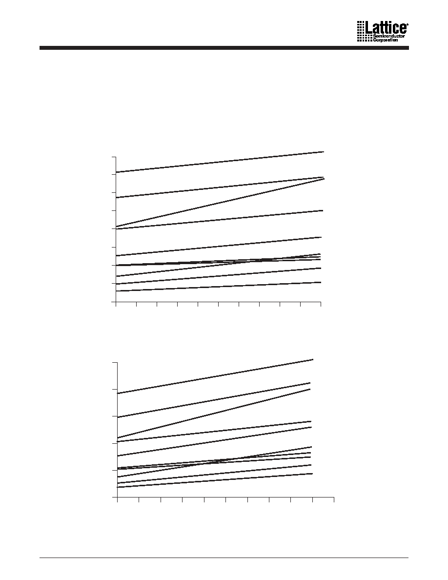
ispMACH 4A Family
41
I
CC
vs. FREQUENCY
These curves represent the typical power consumption for a particular device at system
frequency. The selected "typical" pattern is a 16-bit up-down counter. This pattern fills the device
and exercises every macrocell. Maximum frequency shown uses internal feedback and a D-type
register. Power/Speed are optimized to obtain the highest counter frequency and the lowest
power. The highest frequency (LSBs) is placed in common PAL blocks, which are set to high
power. The lowest frequency signals (MSBs) are placed in a common PAL block and set to
lowest power.
350
300
250
200
150
100
50
0
0
20
40
60
80
100
120
140
160
180
200
V
CC
= 5 V or 3.3 V, T
A
= 25∫ C
I
CC
(mA)
Frequency (MHz)
M4A-32/32
M4A-64/32
M4A-128/64
M4A-256/128
Figure 19. ispMACH 4A I
CC
Curves at High Speed Mode
M4A-256/160
M4A-64/64
M4A-96/48
400
M4A-512/160
M4A-192/96
M4A-384/160
250
200
150
100
50
0
0
20
40
60
80
100
120
140
160
180
200
V
CC
= 5 V or 3.3 V, T
A
= 25∫ C
M4A-32/32
I
CC
(mA)
Frequency (MHz)
M4A-64/32
M4A-128/64
M4A-256/128
Figure 20. ispMACH 4A I
CC
Curves at Low Power Mode
M4A-256/160
M4A-64/64
M4A-96/48
M4A-512/160
M4A-192/96
M4A-384/160

42
ispMACH 4A Family
44-PIN PLCC CONNECTION DIAGRAM (M4A(3,5)-32/32 AND M4A(3,5)-64/32)
Top View
44-Pin PLCC
PIN DESIGNATIONS
CLK/I = Clock or Input
GND = Ground
I/O
= Input/Output
V
CC
= Supply Voltage
TDI
= Test Data In
TCK
= Test Clock
TMS
= Test Mode Select
TDO
= Test Data Out
1 44 43 42
5
4
3
2
6
41 40
7
8
9
10
11
12
13
14
15
16
17
23 24 25 26
19 20 21 22
18
27 28
39
38
37
36
35
34
33
32
31
30
29
I/O5
I/O6
I/O7
TDI
CLK0/I0
GND
TCK
I/O8
I/O9
I/O10
I/O11
A2
A1
A0
B0
B1
B2
B3
D3
D2
D1
D0
C0
C1
C2
B3
B2
B1
B0
B8
B9
B10
A2
A1
A0
A8
A9
A10
A11
I/O27
I/O26
I/O25
I/O24
TDO
GND
CLK1/I1
TMS
I/O23
I/O22
I/O21
I/O12
I/O13
I/O14
I/O15
VCC
GND
I/O16
I/O17
I/O18
I/O19
I/O20
B4
B5
B6
B7
C7
C6
C5
C4
C3
A12
A13
A14
A15
B15
B14
B13
B12
B11
I/O4
I/O3
I/O2
I/O1
I/O0
GND
VCC
I/O31
I/O30
I/O29
I/O28
A3
A4
A5
A6
A7
D7
D6
D5
D4
A3
A4
A5
A6
A7
B7
B6
B5
B4
M4A(3,5)-32/32
M4A(3,5)-32/32
M4A(3,5)-64/32
M4A(3,5)-64/32
M4A(3,5)-64/32
M4A(3,5)-64/32
17466G-026
I/O Cell
PAL Block
C
7

ispMACH 4A Family
43
44-PIN TQFP CONNECTION DIAGRAM (M4A(3,5)-32/32 AND M4A(3,5)-64/32)
Top View
44-Pin TQFP (1.0mm Thickness)
PIN DESIGNATIONS
CLK/I = Clock or Input
GND = Ground
I/O
= Input/Output
V
CC
= Supply Voltage
TDI
= Test Data In
TCK
= Test Clock
TMS
= Test Mode Select
TDO
= Test Data Out
I/O12
I/O13
I/O14
I/O15
VCC
GND
I/O16
I/O17
I/O18
I/O19
I/O20
B4
B5
B6
B7
C7
C6
C5
C4
C3
A12
A13
A14
A15
B15
B14
B13
B12
B11
I/O4
I/O3
I/O2
I/O1
I/O0
GND
VCC
I/O31
I/O30
I/O29
I/O28
A3
A4
A5
A6
A7
D7
D6
D5
D4
A3
A4
A5
A6
A7
B7
B6
B5
B4
I/O27
I/O26
I/O25
I/O24
TDO
GND
CLK1/I1
TMS
I/O23
I/O22
I/O21
D3
D2
D1
D0
C0
C1
C2
B3
B2
B1
B0
B8
B9
B10
I/O5
I/O6
I/O7
TDI
CLK0/I0
GND
TCK
I/O8
I/O9
I/O10
I/O11
A2
A1
A0
B0
B1
B2
B3
A2
A1
A0
A8
A9
A10
A11
1
2
3
4
5
6
7
8
9
10
11
33
32
31
30
29
28
27
26
25
24
23
44
43
42
41
40
39
38
37
36
35
34
12
13
14
15
16
17
18
19
20
21
22
M4A(3,5)-32/32
M4A(3,5)-32/32
M4A(3,5)-64/32
M4A(3,5)-64/32
M4A(3,5)-64/32
M4A(3,5)-64/32
I/O Cell
PAL Block
C
7

44
ispMACH 4A Family
48-PIN TQFP CONNECTION DIAGRAM (M4A(3,5)-32/32 AND M4A(3,5)-64/32)
Top View
48-Pin TQFP (1.4mm Thickness)
PIN DESIGNATIONS
CLK/I = Clock or Input
GND = Ground
I/O
= Input/Output
V
CC
= Supply Voltage
NC
= No Connect
TDI
= Test Data In
TCK
= Test Clock
TMS
= Test Mode Select
TDO
= Test Data Out
I/O12
I/O13
I/O14
I/O15
VCC
NC
GND
I/O16
I/O17
I/O18
I/O19
I/O20
B4
B5
B6
B7
C7
C6
C5
C4
C3
A12
A13
A14
A15
B15
B14
B13
B12
B11
I/O4
I/O3
I/O2
I/O1
I/O0
GND
NC
VCC
I/O31
I/O30
I/O29
I/O28
A3
A4
A5
A6
A7
D7
D6
D5
D4
A3
A4
A5
A6
A7
B7
B6
B5
B4
I/O27
I/O26
I/O25
I/O24
TDO
GND
NC
CLK1/I1
TMS
I/O23
I/O22
I/O21
D3
D2
D1
D0
C0
C1
C2
B3
B2
B1
B0
B8
B9
B10
I/O5
I/O6
I/O7
TDI
CLK0/I0
NC
GND
TCK
I/O8
I/O9
I/O10
I/O11
A2
A1
A0
B0
B1
B2
B3
A2
A1
A0
A8
A9
A10
A11
1
2
3
4
5
6
7
8
9
10
11
12
33
34
35
36
32
31
30
29
28
27
26
25
44
45
46
47
48
43
42
41
40
39
38
37
13
14
15
16
17
18
19
20
21
22
23
24
M4A(3,5)-32/32
M4A(3,5)-32/32
M4A(3,5)-64/32
M4A(3,5)-64/32
M4A(3,5)-64/32
M4A(3,5)-64/32
I/O Cell
PAL Block
C
7
17466G-028

ispMACH 4A Family
45
100-PIN TQFP CONNECTION DIAGRAM (M4A(3,5)-96/48)
Top View
100-Pin TQFP
PIN DESIGNATIONS
CLK/I = Clock or Input
GND = Ground
I
= Input
I/O
= Input/Output
V
CC
= Supply Voltage
NC
= No Connect
TDI
= Test Data In
TCK
= Test Clock
TMS
= Test Mode Select
TDO
= Test Data Out
1
2
3
4
5
6
7
8
9
10
11
12
13
14
15
16
17
18
19
20
21
22
23
24
25
NC
TDI
NC
NC
I/O6
I/O7
I/O8
I/O9
I/O10
I/O11
I0/CLK0
V
CC
GND
I1/CLK1
I/O12
I/O13
I/O14
I/O15
I/O16
I/O17
NC
NC
TMS
TCK
NC
A1
A0
B0
B1
B2
B3
B4
B5
B6
B7
C0
C1
26
27
28
29
30
31
32
33
34
35
36
37
38
39
40
41
42
43
44
45
46
47
48
49
50
GND
NC
NC
I/O18
I/O19
I/O20
I/O21
I/O22
I/O23
NC
I2
NC
NC
GND
V
CC
I3
I/O24
I/O25
I/O26
I/O27
I/O28
I/O29
NC
NC
GND
C2
C3
C4
C5
C6
C7
D7
D6
D5
D4
D3
D2
100
99
98
97
96
95
94
93
92
91
90
89
88
87
86
85
84
83
82
81
80
79
78
77
76
GND
NC
NC
I/O5
I/O4
I/O3
I/O2
I/O1
I/O0
I7
V
CC
GND
NC
NC
I6
NC
I/O47
I/O46
I/O45
I/O44
I/O43
I/O42
NC
NC
GND
A2
A3
A4
A5
A6
A7
F7
F6
F5
F4
F3
F2
75
74
73
72
71
70
69
68
67
66
65
64
63
62
61
60
59
58
57
56
55
54
53
52
51
NC
TDO
NC
NC
NC
I/O41
I/O40
I/O39
I/O38
I/O37
I/O36
I5/CLK3
GND
V
CC
I4/CLK2
I/O35
I/O34
I/O33
I/O32
I/O31
I/O30
NC
NC
NC
NC
F1
F0
E0
E1
E2
E3
E4
E5
E6
E7
D0
D1
17466G-029
I/O Cell
PAL Block
C
7
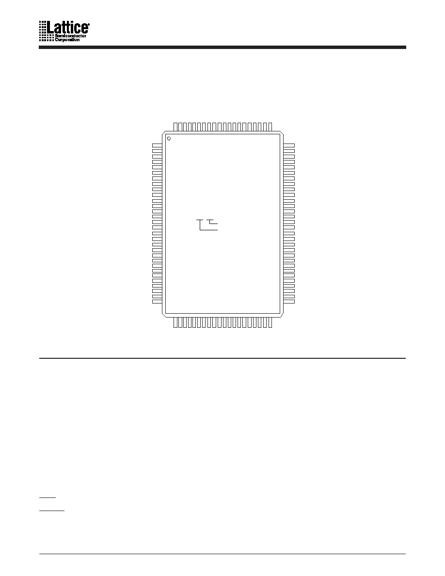
46
ispMACH 4A Family
100-PIN PQFP CONNECTION DIAGRAM (M4A(3,5)-128/64)
Top View
100-Pin PQFP
PIN DESIGNATIONS
I/CLK = Input or Clock
GND = Ground
I
= Input
I/O
= Input/Output
V
CC
= Supply Voltage
TDI
= Test Data In
TCK
= Test Clock
TMS
= Test Mode Select
TDO
= Test Data Out
TRST = Test Reset
ENABLE = Program
I/O7
A
7
A6
A5
A4
A3
A2
A1
A0
D7
D6
D5
D4
D3
D2
D1
D0
I/O6
I/O5
I/O4 I/O3
I/O2
I/O1
I/O0
V
CC
GND
GND V
CC
I/O63
I/O62
I/O61
I/O60
I/O59
I/O58
I/O57
I/O56
H0
H1
H2
H3
H4
H5
H6
H7
GND
GND
TDI
I5
I/O8
I/O9
I/O10
I/O11
I/O12
I/O13
I/O14
I/O15
IO/CLK0
GND
GND
I1/CLK1
I/O16
I/O17
I/O18
I/O19
I/O20
I/O21
I/O22
I/O23
B7
B6
B5
B4
B3
B2
B1
B0
C0
C1
C2
C3
C4
C5
C6
C7
TMS
TCK
GND
GND
28
29
30
4
5
6
7
8
9
10
11
12
13
14
15
16
17
18
19
20
21
22
23
24
25
26
27
1
2
3
99
98
100
31
32
33
34 35
36
37
38
39
40
41
42 43
44
45
46
47
48
49
50
97
96
95
94
93
92
91
90 89
88
87
86
85
84
82
81
83
I/O46
I/O45
I/O44
I/O43
I/O42
I/O41
I/O40
I2
ENABLE
GND
GND
GND
TD0
TRST
I/O55
I/O54
I/O53
I/O52
I/O51
I/O50
I/O49
I/O48
G7
G6
G5
G4
G3
G2
G1
G0
I4/CLK3
GND
GND
I3/CLK2
I/O47
F1
F2
F3
F4
F5
F6
F7
F0
GND
77
76
75
74
73
72
71
70
69
68
67
66
65
64
63
62
61
60
59
58
57
56
55
54
53
52
51
80
79
78
I/O24
I/O25
I/O26
I/O27
I/O28
I/O29
I/O30
I/O31
GND
GND
I/O32
I/O33
I/O34
I/O35
I/O36
I/O37
I/O38
I/O39
E0
E1
E2
E3
E4
E5
E6
E7
VCC
VCC
VCC
VCC
V
CC
V
CC
I/O Cell
PAL Block
C
7
17466G-031

ispMACH 4A Family
47
100-PIN TQFP CONNECTION DIAGRAM (M4A3-64/64 AND M4A(3,5)-128/64)
Top View
100-Pin TQFP
PIN DESIGNATIONS
CLK/I = Clock or Input
GND = Ground
I
= Input
I/O
= Input/Output
V
CC
= Supply Voltage
TDI
= Test Data In
TCK
= Test Clock
TMS
= Test Mode Select
TDO
= Test Data Out
TRST = Test Reset
ENABLE = Program
1
2
3
4
5
6
7
8
9
10
11
12
13
14
15
16
17
18
19
20
21
22
23
24
25
GND
TDI
I/O8
I/O9
I/O10
I/O11
I/O12
I/O13
I/O14
I/O15
I0/CLK0
VCC
GND
I1/CLK1
I/O16
I/O17
I/O18
I/O19
I/O20
I/O21
I/O22
I/O23
TMS
TCK
GND
A1
A3
A5
A7
A9
A11
A13
A15
B15
B13
B11
B9
B7
B5
B3
B1
B7
B6
B5
B4
B3
B2
B1
B0
C0
C1
C2
C3
C4
C5
C6
C7
26
27
28
29
30
31
32
33
34
35
36
37
38
39
40
41
42
43
44
45
46
47
48
49
50
GND
GND
I/O24
I/O25
I/O26
I/O27
I/O28
I/O29
I/O30
I/O31
I2
V
CC
GND
GND
V
CC
I/O32
I/O33
I/O34
I/O35
I/O36
I/O37
I/O38
I/O39
GND
GND
B14
B12
B10
B8
B6
B4
B2
B0
C0
C2
C4
C6
C8
C10
C12
C14
D7
D6
D5
D4
D3
D2
D1
D0
E0
E1
E2
E3
E4
E5
E6
E7
100
99
98
97
96
95
94
93
92
91
90
89
88
87
86
85
84
83
82
81
80
79
78
77
76
GND
GND
I/O7
I/O6
I/O5
I/O4
I/O3
I/O2
I/O1
I/O0
V
CC
GND
GND
V
CC
I5
I/O63
I/O62
I/O61
I/O60
I/O59
I/O58
I/O57
I/O56
GND
GND
A14
A12
A10
A8
A6
A4
A2
A0
D0
D2
D4
D6
D8
D10
D12
D14
A7
A6
A5
A4
A3
A2
A1
A0
H0
H1
H2
H3
H4
H5
H6
H7
75
74
73
72
71
70
69
68
67
66
65
64
63
62
61
60
59
58
57
56
55
54
53
52
51
GND
TDO
TRST
I/O55
I/O54
I/O53
I/O52
I/O51
I/O50
I/O49
I/O48
I4/CLK3
GND
VCC
I3/CLK2
I/O47
I/O46
I/O45
I/O44
I/O43
I/O42
I/O41
I/O40
ENABLE
GND
D1
D3
D5
D7
D9
D11
D13
D15
C15
C13
C11
C9
C7
C5
C3
C1
G7
G6
G5
G4
G3
G2
G1
G0
F0
F1
F2
F3
F4
F5
F6
F7
M4A3-64/64
M4A3-128/64
M4A5-128/64
17466G-032a
I/O Cell
PAL Block
C
7
48
ispMACH 4A Family
100-BALL caBGA CONNECTION DIAGRAM (M4A3-128/64)
Bottom View
100-Ball caBGA
10
9
8
7
6
5
4
3
2
1
A
GND
I/O63
H7
I/O60
H4
I/O57
H1
GND
GND
I/O1
A1
I/O4
A4
I/O7
A7
GND
A
B
TRST
GND
I/O61
H5
I5
VCC
I/O0
A0
I/O6
A6
GND
TDI
I/O15
B7
B
C
I/O53
G5
TDO
I/O62
H6
I/O58
H2
I/O56
H0
I/O2
A2
GND
I/O14
B6
I/O13
B5
I/O12
B4
C
D
I/O50
G2
I/O55
G7
GND
I/O59
H3
I/O3
A3
I/O5
A5
I/O11
B3
I/O10
B2
CLK0/I0
CLK3/I4
I/O9
B1
D
E
I/O49
G1
I/O51
G3
I/O54
G6
VCC
I/O16
C0
I/O20
C4
I/O8
B0
VCC
GND
E
F
GND
VCC
I/O40
F0
I/O52
G4
I/O48
G0
VCC
I/O22
C6
I/O19
C3
I/O17
C1
CLK1/I1
F
G
I/O41
F1
CLK2/I3
I/O42
F2
I/O43
F3
I/O37
E5
I/O35
E3
I/O27
D3
GND
I/O23
C7
I/O18
C2
G
H
I/O44
F4
I/O45
F5
I/O46
F6
GND
I/O34
E2
I/O24
D0
I/O26
D2
I/O30
D6
TCK
I/O21
C5
H
J
I/O47
F7
ENABLE
GND
I/O38
E6
I/O32
E0
VCC
I2
I/O29
D5
GND
TMS
J
K
GND
I/O39
E7
I/O36
E4
I/O33
E1
GND
GND
I/O25
D1
I/O28
D4
I/O31
D7
GND
K
10
9
8
7
6
5
4
3
2
1
PIN DESIGNATIONS
CLK
GND
I
I/O
N/C
VCC
TDI
TCK
TMS
TDO
TRST
ENABLE
=
=
=
=
=
=
=
=
=
=
=
=
I/O Cell
PAL Block
Clock
Ground
Input
Input/Output
No Connect
Supply Voltage
Test Data In
Test Clock
Test Mode Select
Test Data Out
Test Reset
Program
C
7
17466G-100cabga
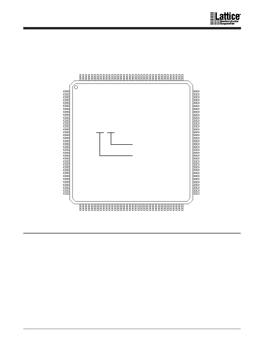
ispMACH 4A Family
49
144-PIN TQFP CONNECTION DIAGRAM (M4A(3,5)-192/96)
Top View
144-Pin TQFP
PIN DESIGNATIONS
CLK
= Clock
GND = Ground
I
= Input
I/O
= Input/Output
V
CC
= Supply Voltage
TDI
= Test Data In
TCK
= Test Clock
TMS
= Test Mode Select
TDO
= Test Data Out
17466G-033
1
2
3
4
5
6
7
8
9
10
11
12
13
14
15
16
17
18
19
20
21
22
23
24
25
26
27
28
29
30
31
32
33
34
35
36
GND
TDI
I/O0
I/O1
I/O2
I/O3
I/O4
I/O5
I/O6
I/O7
I2
I3
V
CC
GND
I4
I/O8
I/O9
I/O10
I/O11
I/O12
I/O13
I/O14
I/O15
GND
V
CC
I/O16
I/O17
I/O18
I/O19
I/O20
I/O21
I/O22
I/O23
TMS
TCK
GND
D7
D6
D5
D4
D3
D2
D1
D0
C7
C6
C5
C4
C3
C2
C1
C0
E7
E6
E5
E4
E3
E2
E1
E0
37
38
39
40
41
42
43
44
45
46
47
48
49
50
51
52
53
54
55
56
57
58
59
60
61
62
63
64
65
66
67
68
69
70
71
72
GND
I/O24
I/O25
I/O26
I/O27
I/O28
I/O29
I/O30
I/O31
I5
I6
I7
CLK1
GND
V
CC
CLK2
I8
I9
I/O32
I/O33
I/O34
I/O35
I/O36
I/O37
I/O38
I/O39
V
CC
GND
I/O40
I/O41
I/O42
I/O43
I/O44
I/O45
I/O46
I/O47
F7
F6
F5
F4
F3
F2
F1
F0
G0
G1
G2
G3
G4
G5
G6
G7
H0
H1
H2
H3
H4
H5
H6
H7
144
143
142
141
140
139
138
137
136
135
134
133
132
131
130
129
128
127
126
125
124
123
122
121
120
119
118
117
116
115
114
113
112
111
110
109
I/O95
I/O94
I/O93
I/O92
I/O91
I/O90
I/O89
I/O88
GND
V
CC
I/O87
I/O86
I/O85
I/O84
I/O83
I/O82
I/O81
I/O80
I1
I0
CLK0
GND
V
CC
CLK3
I15
I14
I13
I/O79
I/O78
I/O77
I/O76
I/O75
I/O74
I/O73
I/O72
GND
B7
B6
B5
B4
B3
B2
B1
B0
A7
A6
A5
A4
A3
A2
A1
A0
L0
L1
L2
L3
L4
L5
L6
L7
108
107
106
105
104
103
102
101
100
99
98
97
96
95
94
93
92
91
90
89
88
87
86
85
84
83
82
81
80
79
78
77
76
75
74
73
GND
TDO
NC
I/O71
I/O70
I/O69
I/O68
I/O67
I/O66
I/O65
I/O64
I12
V
CC
GND
I11
I10
I/O63
I/O62
I/O61
I/O60
I/O59
I/O58
I/O57
I/O56
GND
V
CC
I/O55
I/O54
I/O53
I/O52
I/O51
I/O50
I/O49
I/O48
NC
GND
K0
K1
K2
K3
K4
K5
K6
K7
J0
J1
J2
J3
J4
J5
J6
J7
I0
I1
I2
I3
I4
I5
I6
I7
I/O Cell
PAL Block
C
7
50
ispMACH 4A Family
144-BALL FPBGA CONNECTION DIAGRAM (M4A3-192/96)
Bottom View
144-Ball fpBGA
12
11
10
9
8
7
6
5
4
3
2
1
A
GND
I/O72
L7
I/O76
L3
I13
GBCLK3
I0
I/O82
A2
I/O86
A6
I/O88
B0
I/O93
B5
I/O95
B7
GND
A
B
GND
I/O73
L6
I/O77
L2
I/O79
L0
VCC
I1
I/O83
A3
I/O87
A7
I/O90
B2
I/O94
B6
I/O0
D7
TDI
B
C
GND
TDO
I/O74
L5
I14
GND
I/O80
A0
I/O84
A4
GND
I/O92
B4
I/O1
D6
I/O4
D3
I/O3
D4
C
D
I/O67
K4
I/O69
K2
I/O71
K0
I/O75
L4
GBCLK0
I/O81
A1
VCC
I/O91
B3
I/O2
D5
I2
I/O6
D1
I/O7
D0
D
E
I12
I/O64
K7
I/O66
K5
I/O70
K1
I/O78
L1
I/O85
A5
I/O89
B1
I/O5
D2
I/O8
C7
I4
GND
VCC
E
F
I10
I11
GND
I/065
K6
I/O68
K3
I15
I3
GND
I/O12
C3
I/O11
C4
I/O10
C5
I/O9
C6
F
G
I/O60
J3
I/O61
J2
I/O62
J1
I/O63
J0
VCC
GND
I7
I/O20
E3
I/O17
E6
I/O15
C0
I/O14
C1
I/O13
C2
G
H
I/O56
J7
I/O57
J6
I/O58
J5
I/O59
J4
I/O53
I2
I/O41
H1
I/O37
G5
I/O30
F1
I/O22
E1
I/O18
E5
I/O16
E7
VCC
H
J
I/O55
I0
I/O54
I1
VCC
I/O50
I5
I/O43
H3
VCC
I/O33
G1
GBCLK2
I/O27
F4
I/O23
E0
I/O21
E2
I/O19
E4
J
K
I/O51
I4
I/O52
I3
I/O49
I6
I/O44
H4
GND
I/O36
G4
I/O32
G0
VCC
I6
I/O26
F5
TCK
TMS
K
L
GND
I/O48
I7
I/O46
H6
I/O42
H2
I/O39
G7
I/O35
G3
I9
GND
I/O31
F0
I/O29
F2
I/O25
F6
GND
L
M
GND
I/O47
H7
I/O45
H5
I/O40
H0
I/O38
G6
I/O34
G2
I8
GBCLK1
I5
I/O28
F3
I/O24
F7
GND
M
12
11
10
9
8
7
6
5
4
3
2
1
PIN DESIGNATIONS
CLK
GND
I
I/O
N/C
VCC
TDI
TCK
TMS
TDO
=
=
=
=
=
=
=
=
=
=
I/O Cell
PAL Block
Clock
Ground
Input
Input/Output
No Connect
Supply Voltage
Test Data In
Test Clock
Test Mode Select
Test Data Out
C
7
m4a3.192.96_144bga

ispMACH 4A Family
51
208-PIN PQFP CONNECTION DIAGRAM (M4A(3,5)-256/128 AND
M4A3-256/160)
Top View
208-Pin PQFP
C7
C6
C5
C4
C3
C2
C1
C0
D7
D6
D5
D4
D3
D2
D1
D0
E0
E1
E2
E3
E4
E5
E6
E7
F0
F1
F2
F3
F4
F5
F6
F7
GND
TDI
I/O16
I/O17
I/O18
I/O19
I/O20
I/O21
I/O22
I/O23
VCC
GND
I/O24
I/O25
I/O26
I/O27
I/O28
I/O29
I/O30
I/O31
I2
I3
GND
VCC
VCC
GND
GND
VCC
VCC
GND
I4
I/O32
I/O33
I/O34
I/O35
I/O36
I/O37
I/O38
I/O39
GND
VCC
I/O40
I/O41
I/O42
I/O43
I/O44
I/O45
I/O46
I/O47
TMS
TCK
GND
GND
I/O48
I/O49
I/O50
I/O51
I/O52
I/O53
I/O54
I/O55
GND
VCC
I/O56
I/O57
I/O58
I/O59
I/O60
I/O61
I/O62
I/O63
I5
I6
CLK1
VCC
GND
GND
VCC
VCC
GND
GND
VCC
CLK2
I7
I8
I/O64
I/O65
I/O66
I/O67
I/O68
I/O69
I/O70
I/O71
VCC
GND
I/O72
I/O73
I/O74
I/O75
I/O76
I/O77
I/O78
I/O79
GND
1
2
3
4
5
6
7
8
9
10
11
12
13
14
15
16
17
18
19
20
21
22
23
24
25
26
27
28
29
30
31
32
33
34
35
36
37
38
39
40
41
42
43
44
45
46
47
48
49
50
51
52
G7
G6
G5
G4
G3
G2
G1
G0
H7
H6
H5
H4
H3
H2
H1
H0
I0
I1
I2
I3
I4
I5
I6
I7
J0
J1
J2
J3
J4
J5
J6
J7
53
54
55
56
57
58
59
60
61
62
63
64
65
66
67
68
69
70
71
72
73
74
75
76
77
78
79
80
81
82
83
84
85
86
87
88
89
90
91
92
93
94
95
96
97
98
99
100
101
102
103
104
N7
N6
N5
N4
N3
N2
N1
N0
M7
M6
M5
M4
M3
M2
M1
M0
L0
L1
L2
L3
L4
L5
L6
L7
K0
K1
K2
K3
K4
K5
K6
K7
B7
B6
B5
B4
B3
B2
B1
B0
A7
A6
A5
A4
A3
A2
A1
A0
P0
P1
P2
P3
P4
P5
P6
P7
O0
O1
O2
O3
O4
O5
O6
O7
GND
I/O15
I/O14
I/O13
I/O12
I/O1
1
I/O10
I/O9
I/O8
GND
VCC
I/O7
I/O6
I/O5
I/O4
I/O3
I/O2
I/O1
I/O0
I1
I0
CLK0
VCC
GND
GND
VCC
VCC
GND
GND
VCC
CLK3
I13
I12
I/O127
I/O126
I/O125
I/O124
I/O123
I/O122
I/O121
I/O120
VCC
GND
I/O1
19
I/O1
18
I/O1
17
I/O1
16
I/O1
15
I/O1
14
I/O1
13
I/O1
12
GND
GND
TDO
TRST
I/O111
I/O110
I/O109
I/O108
I/O107
I/O106
I/O105
I/O104
VCC
GND
I/O103
I/O102
I/O101
I/O100
I/O99
I/O98
I/O97
I/O96
I11
GND
VCC
VCC
GND
GND
VCC
VCC
GND
I10
I9
I/O95
I/O94
I/O93
I/O92
I/O91
I/O90
I/O89
I/O88
GND
VCC
I/O87
I/O86
I/O85
I/O84
I/O83
I/O82
I/O81
I/O80
ENABLE
GND
156
155
154
153
152
151
150
149
148
147
146
145
144
143
142
141
140
139
138
137
136
135
134
133
132
131
130
129
128
127
126
125
124
123
122
121
120
119
118
117
116
115
114
113
112
111
110
109
108
107
106
105
208
207
206
205
204
203
202
201
200
199
198
197
196
195
194
193
192
191
190
189
188
187
186
185
184
183
182
181
180
179
178
177
176
175
174
173
172
171
170
169
168
167
166
165
164
163
162
161
160
159
158
157
RECOMMEND TO TIE TO VCC
M4A(3, 5)-
256/128
RECOMMEND TO TIE TO GND
PIN DESIGNATIONS
CLK
GND
I
I/O
N/C
VCC
TDI
TCK
TMS
TDO
TRST
ENABLE
=
=
=
=
=
=
=
=
=
=
=
=
I/O Cell
PAL Block
Clock
Ground
Input
Input/Output
No Connect
Supply Voltage
Test Data In
Test Clock
Test Mode Select
Test Data Out
Test Reset
Program
C
7
M4A3-256/160
GND
TDI
I/O20
I/O21
I/O22
I/O23
I/O24
I/O25
I/O26
I/O27
VCC
GND
I/O28
I/O29
I/O30
I/O31
I/O32
I/O33
I/O34
I/O35
I/O36
I/O37
GND
VCC
I/O38
I/O39
I/O40
I/O41
I/O42
GND
I/O43
I/O44
I/O45
I/O46
I/O47
I/O48
I/O49
I/O50
I/O51
GND
VCC
I/O52
I/O53
I/O54
I/O55
I/O56
I/O57
I/O58
I/O59
TMS
TCK
GND
C15
C14
C13
C12
C11
C10
C9
C8
C7
C6
C5
C4
C3
C2
C1
C0
D14
D12
D6
D4
E0
E2
E6
E10
F0
F1
F2
F3
F4
F5
F6
F7
F8
F9
F10
F11
F12
F13
F14
F15
GND
TDO
NC
I/O139
I/O138
I/O137
I/O136
I/O135
I/O134
I/O133
I/O132
VCC
GND
I/O131
I/O130
I/O129
I/O128
I/O127
I/O126
I/O125
I/O124
I/O123
GND
I/O122
I/O121
I/O120
I/O119
I/O118
VCC
GND
I/O117
I/O116
I/O115
I/O114
I/O113
I/O112
I/O111
I/O110
I/O109
I/O108
GND
VCC
I/O107
I/O106
I/O105
I/O104
I/O103
I/O102
I/O101
I/O100
NC
GND
N15
N14
N13
N12
N11
N10
N9
N8
N7
N6
N5
N4
N3
N2
N1
N0
M10
M6
M2
M0
L4
L6
L12
L14
K0
K1
K2
K3
K4
K5
K6
K7
K8
K9
K10
K11
K12
K13
K14
K15
GND
I/O60
I/O61
I/O62
I/O63
I/O64
I/O65
I/O66
I/O67
GND
VCC
I/O68
I/O69
I/O70
I/O71
I/O72
I/O73
I/O74
I/O75
I/O76
I/O77
CLK1
VCC
GND
I/O78
I/O79
I/O80
I/O81
GND
VCC
CLK2
I/O82
I/O83
I/O84
I/O85
I/O86
I/O87
I/O88
I/O89
I/O90
I/O91
VCC
GND
I/O92
I/O93
I/O94
I/O95
I/O96
I/O97
I/O98
I/O99
GND
G15
G14
G13
G12
G1
1
G10
G9
G8
G7
G6
G5
G4
G3
G2
G1
G0
H14
H12
H6
H4
I4
I6
I12
I14
J0
J1
J2
J3
J4
J5
J6
J7
J8
J9
J10
J1
1
J12
J13
J14
J15
GND
I/O19
I/O18
I/O17
I/O16
I/O15
I/O14
I/O13
I/O12
GND
VCC
I/O1
1
I/O10
I/O9
I/O8
I/O7
I/O6
I/O5
I/O4
I/O3
I/O2
CLK0
VCC
GND
I/O1
I/O0
I/O159
I/O158
GND
VCC
CLK3
I/O157
I/O156
I/O155
I/O154
I/O153
I/O152
I/O151
I/O150
I/O149
I/O148
VCC
GND
I/O147
I/O146
I/O145
I/O144
I/O143
I/O142
I/O141
I/O140
GND
B15
B14
B13
B12
B1
1
B10
B9
B8
B7
B6
B5
B4
B3
B2
B1
B0
A14
A12
A6
A4
P4
P6
P12
P14
O0
O1
O2
O3
O4
O5
O6
O7
O8
O9
O10
O1
1
O12
O13
O14
O15
17466G-044
52
ispMACH 4A Family
208-PIN PQFP CONNECTION DIAGRAM (M4A3-384/160 AND M4A3-512/160)
Top View
208-Pin PQFP
1
2
3
4
5
6
7
8
9
10
11
12
13
14
15
16
17
18
19
20
21
22
23
24
25
26
27
28
29
30
31
32
33
34
35
36
37
38
39
40
41
42
43
44
45
46
47
48
49
50
51
52
53
54
55
56
57
58
59
60
61
62
63
64
65
66
67
68
69
70
71
72
73
74
75
76
77
78
79
80
81
82
83
84
85
86
87
88
89
90
91
92
93
94
95
96
97
98
99
100
101
102
103
104
156
155
154
153
152
151
150
149
148
147
146
145
144
143
142
141
140
139
138
137
136
135
134
133
132
131
130
129
128
127
126
125
124
123
122
121
120
119
118
117
116
115
114
113
112
111
110
109
108
107
106
105
208
207
206
205
204
203
202
201
200
199
198
197
196
195
194
193
192
191
190
189
188
187
186
185
184
183
182
181
180
179
178
177
176
175
174
173
172
171
170
169
168
167
166
165
164
163
162
161
160
159
158
157
M4A3-512/160
PIN DESIGNATIONS
CLK
GND
I
I/O
N/C
VCC
TDI
TCK
TMS
TDO
=
=
=
=
=
=
=
=
=
=
I/O Cell
PAL Block
Clock
Ground
Input
Input/Output
No Connect
Supply Voltage
Test Data In
Test Clock
Test Mode Select
Test Data Out
C
7
GND
TDO
NC
I/O137
I/O136
I/O135
I/O134
I/O133
I/O132
I/O131
I/O130
VCC
GND
I/O129
I/O128
I/O127
I/O126
I/O125
I/O124
I/O123
I/O122
I/O121
GND
I/O120
I/O119
I/O118
I/O117
I/O116
VCC
GND
I/O115
I/O114
I/O113
I/O112
I/O111
I/O110
I/O109
I/O108
I/O107
I/O106
GND
VCC
I/O105
I/O104
I/O103
I/O102
I/O101
I/O100
I/O99
I/O98
NC
GND
GND
I/O17
I/O16
I/O15
I/O14
I/O13
I/O12
I/O1
1
I/O10
GND
VCC
I/O9
I/O8
I/O7
I/O6
I/O5
I/O4
I/O3
I/O2
I/O1
I/O0
CLK0
VCC
GND
I/O159
I/O158
I/O157
I/O156
GND
VCC
CLK3
I/O155
I/O154
I/O153
I/O152
I/O151
I/O150
I/O149
I/O148
I/O147
I/O146
VCC
GND
I/O145
I/O144
I/O143
I/O142
I/O141
I/O140
I/O139
I/O138
GND
GND
I/O58
I/O59
I/O60
I/O61
I/O62
I/O63
I/O64
I/O65
GND
VCC
I/O66
I/O67
I/O68
I/O69
I/O70
I/O71
I/O72
I/O73
I/O74
I/O75
CLK1
VCC
GND
I/O76
I/O77
I/O78
I/O79
GND
VCC
CLK2
I/O80
I/O81
I/O82
I/O83
I/O84
I/O85
I/O86
I/O87
I/O88
I/O89
VCC
GND
I/O90
I/O91
I/O92
I/O93
I/O94
I/O95
I/O96
I/O97
GND
GND
TDI
I/O18
I/O19
I/O20
I/O21
I/O22
I/O23
I/O24
I/O25
VCC
GND
I/O26
I/O27
I/O28
I/O29
I/O30
I/O31
I/O32
I/O33
I/O34
I/O35
GND
VCC
I/O36
I/O37
I/O38
I/O39
I/O40
GND
I/O41
I/O42
I/O43
I/O44
I/O45
I/O46
I/O47
I/O48
I/O49
GND
VCC
I/O50
I/O51
I/O52
I/O53
I/O54
I/O55
I/O56
I/O57
TMS
TCK
GND
C7
C6
C5
C4
C3
C2
C1
C0
F7
F6
F5
F4
F3
F2
F1
F0
E7
E5
E2
E0
H0
H2
H3
H5
G0
G1
G2
G3
G4
G5
G6
G7
J0
J1
J2
J3
J4
J5
J6
J7
GND
TDI
I/O18
I/O19
I/O20
I/O21
I/O22
I/O23
I/O24
I/O25
VCC
GND
I/O26
I/O27
I/O28
I/O29
I/O30
I/O31
I/O32
I/O33
I/O34
I/O35
GND
VCC
I/O36
I/O37
I/O38
I/O39
I/O40
GND
I/O41
I/O42
I/O43
I/O44
I/O45
I/O46
I/O47
I/O48
I/O49
GND
VCC
I/O50
I/O51
I/O52
I/O53
I/O54
I/O55
I/O56
I/O57
TMS
TCK
GND
GND
I/O58
I/O59
I/O60
I/O61
I/O62
I/O63
I/O64
I/O65
GND
VCC
I/O66
I/O67
I/O68
I/O69
I/O70
I/O71
I/O72
I/O73
I/O74
I/O75
CLK1
VCC
GND
I/O76
I/O77
I/O78
I/O79
GND
VCC
CLK2
I/O80
I/O81
I/O82
I/O83
I/O84
I/O85
I/O86
I/O87
I/O88
I/O89
VCC
GND
I/O90
I/O91
I/O92
I/O93
I/O94
I/O95
I/O96
I/O97
GND
K7
K6
K5
K4
K3
K2
K1
K0
I7
I6
I5
I4
I3
I2
I1
I0
L7
L6
L4
L1
M1
M4
M6
M7
P0
P1
P2
P3
P4
P5
P6
P7
N0
N1
N2
N3
N4
N5
N6
N7
B7
B6
B5
B4
B3
B2
B1
B0
D7
D6
D5
D4
D3
D2
D1
D0
A7
A6
A4
A1
HX1
HX4
HX6
HX7
EX0
EX1
EX2
EX3
EX4
EX5
EX6
EX7
GX0
GX1
GX2
GX3
GX4
GX5
GX6
GX7
GND
I/O17
I/O16
I/O15
I/O14
I/O13
I/O12
I/O1
1
I/O10
GND
VCC
I/O9
I/O8
I/O7
I/O6
I/O5
I/O4
I/O3
I/O2
I/O1
I/O0
CLK0
VCC
GND
I/O159
I/O158
I/O157
I/O156
GND
VCC
CLK3
I/O155
I/O154
I/O153
I/O152
I/O151
I/O150
I/O149
I/O148
I/O147
I/O146
VCC
GND
I/O145
I/O144
I/O143
I/O142
I/O141
I/O140
I/O139
I/O138
GND
M4A3-384/160
FX7
FX6
FX5
FX4
FX3
FX2
FX1
FX0
CX7
CX6
CX5
CX4
CX3
CX2
CX1
CX0
DX5
DX3
DX2
DX0
AX0
AX2
AX5
AX7
BX0
BX1
BX2
B3X
BX4
BX5
BX6
BX7
O0
O1
O2
O3
O4
O5
O6
O7
GND
TDO
NC
I/O137
I/O136
I/O135
I/O134
I/O133
I/O132
I/O131
I/O130
VCC
GND
I/O129
I/O128
I/O127
I/O126
I/O125
I/O124
I/O123
I/O122
I/O121
GND
I/O120
I/O119
I/O118
I/O117
I/O116
VCC
GND
I/O115
I/O114
I/O113
I/O112
I/O111
I/O110
I/O109
I/O108
I/O107
I/O106
GND
VCC
I/O105
I/O104
I/O103
I/O102
I/O101
I/O100
I/O99
I/O98
NC
GND
F7
F6
F5
F4
F3
F2
F1
F0
G7
G6
G5
G4
G3
G2
G1
G0
E7
E5
E2
E0
L0
L2
L3
L5
J0
J1
J2
J3
J4
J5
J6
J7
K0
K1
K2
K3
K4
K5
K6
K7
O7
O6
O5
O4
O3
O2
O1
O0
N7
N6
N5
N4
N3
N2
N1
N0
P7
P6
P4
P1
AX1
AX4
AX6
AX7
CX0
CX1
CX2
CX3
CX4
CX5
CX6
CX7
BX0
BX1
BX2
BX3
BX4
BX5
BX6
BX7
KX7
KX6
KX5
KX4
KX3
KX2
KX1
KX0
JX7
JX6
JX5
JX4
JX3
JX2
JX1
JX0
LX5
LX3
LX2
LX0
EX0
EX2
EX5
EX7
GX0
GX1
GX2
GX3
GX4
GX5
GX6
GX7
FX0
FX1
FX2
FX3
FX4
FX5
FX6
FX7
B7
B6
B5
B4
B3
B2
B1
B0
C7
C6
C5
C4
C3
C2
C1
C0
A7
A6
A4
A1
PX1
PX4
PX6
PX7
NX0
NX1
NX2
NX3
NX4
NX5
NX6
NX7
OX0
OX1
OX2
OX3
OX4
OX5
OX6
OX7
17466Ga-044
ispMACH 4A Family
53
256-BALL BGA CONNECTION DIAGRAM (M4A3-256/128)
Bottom View
256-Ball BGA
GND
GND
I/O116
O3
I/O120
P7
I/O123
P4
GND
I12
GND
N/C
GND
N/C
N/C
GND
I1
A
B
C
D
E
F
G
H
J
K
L
M
N
P
R
T
U
V
W
Y
A
B
C
D
E
F
G
H
J
K
L
M
N
P
R
T
U
V
W
Y
N/C
I/O113
O6
N/C
I/O117
O2
I/O119
O0
I/O122
P5
I/O125
P2
I/O127
P0
N/C
CLK3
CLK0
N/C
I/O0
A0
I/O1
A1
GND
N/C
VCC
I/O112
O7
I/O114
O5
I/O118
O1
I/O121
P6
I/O126
P1
N/C
N/C
N/C
N/C
I/O2
A2
I/O6
A6
I/O108
N4
I/O109
N5
TRST
VCC
TDI
I/O115
O4
VCC
I/O124
P3
I13
N/C
N/C
I0
I/O3
A3
VCC
I/O105
N1
I/O106
N2
I/O111
N7
VCC
GND
I/O103
M7
I/O107
N3
I/O110
N6
I/O100
M4
I/O102
M6
I/O104
N0
VCC
I/O96
M0
I/O98
M2
I/O101
M5
N/C
GND
N/C
I/O97
M1
I/O99
M3
GND
I11
N/C
N/C
GND
N/C
I10
I9
GND
N/C
I/O94
L1
I/O92
L3
GND
I/O82
K5
VCC
I/O79
J7
I/O77
J5
I/O73
J1
I/O70
I6
I/O66
I2
N/C
N/C
N/C
N/C
I/O61
H2
I/O57
H6
GND
20
19
18
17
16
15
14
13
12
11
10
9
I/O95
L0
I/O93
L2
I/O90
L5
N/C
8
I/O91
L4
I/O89
L6
I/O86
K1
VCC
7
GND
I/O88
L7
I/O84
K3
I/O81
K6
6
I/O87
K0
I/O85
K2
I/O80
K7
VCC
5
N/C
I/O83
K4
ENABLE
VCC
TDO
I/O76
J4
VCC
I/O67
I3
I7
N/C
N/C
I6
I/O60
H3
VCC
4
3
GND
N/C
I/O78
J6
I/O75
J3
I/O72
J0
I/O69
I5
I/O65
I1
I/O64
I0
N/C
CLK2
CLK1
I/O63
H0
I/O59
H4
I/O58
H5
2
1
20
19
18
17
16
15
14
13
12
11
10
9
8
7
6
5
4
3
2
1
GND
I/O74
J2
I/O71
I7
I/O68
I4
GND
I8
GND
N/C
N/C
GND
I/O62
H1
GND
I5
GND
I/O4
A4
I/O7
A7
I/O5
A5
I/O8
B0
I/O11
B3
I/O9
B1
I/O12
B4
I/O15
B7
N/C
TCK
VCC
VCC
I/O18
C5
VCC
I/O24
D7
I/O29
D2
I2
N/C
I/O35
E3
I/O54
G1
I/O50
G5
I/O48
G7
N/C
VCC
N/C
VCC
I/O51
G4
TMS
VCC
I/O56
H7
I/O55
G0
I/O53
G2
GND
N/C
N/C
I/O10
B2
GND
GND
I/O13
B5
I/O14
B6
GND
VCC
N/C
GND
I/O16
C7
N/C
N/C
I/O17
C6
I/O19
C4
I/O20
C3
I/O21
C2
I/O22
C1
GND
I/O23
C0
I/O25
D6
I/O26
D5
I/O27
D4
I/O28
D3
I/O30
D1
I/O31
D0
N/C
GND
I3
N/C
GND
N/C
I4
GND
I/O33
E1
N/C
GND
VCC
N/C
GND
I/O37
E5
I/O34
E2
I/O32
E0
I/O41
F1
I/O38
E6
I/O36
E4
I/O43
F3
I/O39
E7
GND
I/O46
F6
I/O42
F2
I/O40
F0
I/O47
F7
I/O45
F5
I/O44
F4
I/O52
G3
I/O49
G6
N/C
N/C
GND
GND
PIN DESIGNATIONS
CLK
GND
I
I/O
N/C
VCC
TDI
TCK
TMS
TDO
TRST
ENABLE
=
=
=
=
=
=
=
=
=
=
=
=
I/O Cell
PAL Block
Clock
Ground
Input
Input/Output
No Connect
Supply Voltage
Test Data In
Test Clock
Test Mode Select
Test Data Out
Test Reset
Program
C
7
17466G-045

54
ispMACH 4A Family
256-BALL fpBGA CONNECTION DIAGRAM (M4A3-256/192)
Bottom View
256-Ball fpBGA
PIN DESIGNATIONS
CLK
GND
I
I/O
N/C
VCC
TDI
TCK
TMS
TDO
=
=
=
=
=
=
=
=
=
=
I/O Cell
PAL Block
Clock
Ground
Input
Input/Output
No Connect
Supply Voltage
Test Data In
Test Clock
Test Mode Select
Test Data Out
C
7
16
15
14
13
12
11
10
9
8
7
6
5
4
3
2
1
A
I/O167
N15
I/O181
O13
I/O180
O12
I/O177
O9
I/O174
O6
I/O172
O4
I/O191
P14
I/O186
P4
I/O1
A2
I/O3
A6
GCLK0
I/O9
B1
I/O13
B5
I/O15
B7
I/O18
B10
I/O20
B12
A
B
I/O165
N13
I/O166
N14
I/O182
O14
I/O179
O11
I/O175
O7
I/O173
O5
I/O168
O0
I/O187
P6
I/O0
A0
I/O5
A10
I/O7
A14
I/O10
B2
I/O16
B8
I/O19
B11
I/O21
B13
NC
B
C
I/O163
N11
I/O164
N12
NC
I/O183
O15
I/O178
O10
I/O170
O2
I/O171
O3
I/O189
P10
I/O184
P0
I/O6
A12
I/O12
B4
I/O14
B6
I/O23
B15
I/O22
B14
TDI
I/O39
C15
C
D
I/O158
N6
I/O159
N7
TDO
GND
GND
VCC
GND
VCC
GND
GND
VCC
GND
VCC
I/O17
B9
I/O38
C14
I/O37
C13
D
E
I/O156
N4
NC
I/O162
N10
VCC
I/O160
N8
I/O161
N9
I/O190
P12
GCLK3 I/O188
P8
I/O2
A4
I/O8
B0
NC
GND
I/O36
C12
I/O35
C11
I/O31
C7
E
F
I/O152
N0
I/O157
N5
I/O155
N3
GND
I/O154
N2
I/O153
N1
I/O176
O8
I/O169
O1
I/O185
P2
I/O4
A8
I/O11
B3
I/O34
C10
VCC
I/O32
C8
I/O30
C6
I/O29
C5
F
G
I/O147
M6
I/O150
M12
I/O149
M10
VCC
I/O148
M8
I/O151
M14
VCC
GND
GND
VCC
I/O33
C9
I/O28
C4
GND
I/O26
C2
I/O25
C1
I/O47
D14
G
H
I/O144
M0
I/O146
M4
I/145
OM2
GND
I/O136
L0
I/O137
L2
GND
VCC
VCC
GND
I/O27
C3
I/O24
C0
VCC
I/O44
D8
I/O43
D6
I/O42
D4
H
J
I/O138
L4
I/O139
L6
I/O140
L8
GND
I/O142
L12
I/O141
L10
GND
VCC
VCC
GND
I/O46
D12
I/O45
D10
GND
I/O49
E2
I/O48
E0
I/O50
E4
J
K
I/O143
L14
I/O120
K0
I/O121
K1
VCC
I/O123
K3
I/O122
K2
VCC
GND
GND
VCC
I/O41
D2
I/O40
D0
VCC
I/O55
E14
I/O54
E12
I/O56
F0
K
L
I/O124
K4
I/O125
K5
I/O127
K7
GND
I/O130
K10
I/O126
K6
I/O98
I4
I/O91
H6
I/O75
G3
I/O77
G5
I/O52
E8
I/O51
E6
GND
I/O59
F3
I/O60
F4
I/O57
F1
L
M
I/O128
K8
I/O129
K9
I/O131
K11
GND
I/O107
J3
I/O105
J1
I/O100
I8
I/O90
H4
I/O74
G2
I/O80
G8
I/O83
G11
I/O53
E10
VCC
I/O68
F12
I/O63
F7
I/O58
F2
M
N
I/O132
K12
I/O133
K13
I/O135
K15
VCC
GND
VCC
GND
VCC
GND
GND
VCC
GND
GND
TCK
I/O64
F8
I/O61
F5
N
P
I/O134
K14
I/O117
J13
I/O118
J14
I/O119
J15
I/O108
J4
I/O106
J2
I/O101
I10
I/O89
H2
I/O93
H10
I/O94
H12
I/O79
G7
I/O84
G12
I/O87
G15
TMS
I/O65
F9
I/O62
F6
P
R
I/O116
J12
I/O115
J11
I/O112
J8
I/O111
J7
I/O104
J0
I/O102
I12
I/O99
I6
I/O96
I0
I/O92
H8
I/O72
G0
I/O76
G4
I/O81
G9
I/O85
G13
I/O71
F15
I/O67
F11
I/O66
F10
R
T
I/O114
J10
I/O113
J9
I/O110
J6
I/O109
J5
I/O103
I14
GCLK2
I/O97
I2
I/O88
H0
GCLK1
I/O95
H14
I/O73
G1
I/O78
G6
I/O82
G10
I/O86
G14
I/O70
F14
I/O69
F13
T
16
15
14
13
12
11
10
9
8
7
6
5
4
3
2
1
17466G-047
ispMACH 4A Family
55
256-BALL BGA CONNECTION DIAGRAM - (M4A3-384/192)
Bottom View
256-Ball BGA
GND
GND
I/O0
GX6
I/O1
EX7
I/O2
EX0
GND
I/O3
HX6
GND
I/O4
HX0
GND
I/O5
A2
I/O6
A4
GND
I/O7
D2
A
B
C
D
E
F
G
H
J
K
L
M
N
P
R
T
U
V
W
Y
A
B
C
D
E
F
G
H
J
K
L
M
N
P
R
T
U
V
W
Y
I/O11
FX7
I/O12
GX7
I/O13
GX5
I/O14
GX3
I/O15
GX0
I/O16
EX1
I/O17
EX4
I/O18
HX5
I/O19
HX1
CLK3
CLK0
I/O20
A3
I/O21
A7
I/O22
D3
GND
I/O28
FX5
VCC
I/O29
GX4
I/O30
GX1
I/O31
EX6
I/O32
EX5
I/O33
EX2
I/O34
HX4
I/O35
HX2
I/O36
A0
I/O37
A5
I/O38
D0
I/O39
D4
I/O44
FX6
I/O45
FX3
I/O46
FX4
VCC
TDI
I/O47
GX2
VCC
I/O48
EX3
I/O49
HX7
I/O50
HX3
I/O51
A1
I/O52
A6
I/O53
D1
VCC
I/O58
CX6
I/O59
CX7
I/O60
FX2
VCC
GND
I/O64
CX5
I/O65
FX1
I/O66
FX0
I/O70
CX2
I/O71
CX3
I/O72
CX4
VCC
I/O76
DX6
I/O77
DX7
I/O78
CX0
I/O79
CX1
GND
I/O84
DX5
I/O85
DX4
I/O86
DX3
GND
I/O90
DX2
I/O91
DX1
I/O92
DX0
GND
I/O96
AX0
I/O97
AX1
I/O98
AX2
GND
I/O102
AX3
I/O103
AX4
I/O104
AX7
GND
I/O148
O6
VCC
I/O149
N4
I/O150
N2
I/O151
N0
I/O152
P4
I/O153
P1
I/O154
M5
I/O155
M1
I/O156
L4
I/O157
L5
I/O158
I0
I/O159
I4
GND
20
19
18
17
16
15
14
13
12
11
10
9
I/O108
AX5
I/O109
AX6
I/O110
BX2
I/O111
B3X
8
I/O116
BX0
I/O117
BX1
I/O118
BX5
VCC
7
GND
I/O122
BX4
I/O123
O0
I/O124
O2
6
I/O128
BX7
I/O129
BX6
I/O130
O1
VCC
5
I/O134
O3
I/O135
O4
I/O136
O5
VCC
TDO
I/O137
N1
VCC
I/O138
P2
I/O139
M6
I/O140
M0
I/O141
L3
I/O142
L6
I/O143
I5
VCC
4
3
GND
I/O164
O7
I/O165
N7
I/O166
N5
I/O167
N3
I/O168
P5
I/O169
P3
I/O170
P0
I/O171
M4
CLK2
CLK1
I/O172
L0
I/O173
L7
I/O174
I1
2
1
20
19
18
17
16
15
14
13
12
11
10
9
8
7
6
5
4
3
2
1
GND
I/O181
N6
I/O182
P7
I/O183
P6
GND
I/O184
M7
GND
I/O185
M3
I/O186
M2
GND
I/O187
L1
GND
I/O188
L2
GND
I/O8
B3
I/O9
B4
I/O23
D5
I/O24
B0
I/O25
B1
I/O40
D6
I/O41
B7
I/O42
B6
I/O54
D7
TCK
VCC
VCC
I/O67
C0
VCC
I/O80
F0
I/O87
E5
I/O93
E2
I/O99
H2
I/O105
H5
I/O160
K0
I/O161
K4
I/O162
K7
I/O112
G0
VCC
I/O125
J1
VCC
I/O144
K5
TMS
VCC
I/O175
I3
I/O176
K1
I/O177
K2
GND
I/O189
I2
I/O190
I6
I/O10
B5
GND
GND
I/O26
B2
I/O27
C7
GND
VCC
I/O43
C6
GND
I/O55
C5
I/O56
C3
I/O57
C4
I/O61
C2
I/O62
F7
I/O63
F6
I/O68
C1
I/O69
F5
GND
I/O73
F4
I/O74
F3
I/O75
F2
I/O81
F1
I/O82
E7
I/O83
E6
I/O88
E4
I/O89
E3
GND
I/O94
E1
I/O95
E0
GND
I/O100
H1
I/O101
H0
GND
I/O106
H4
I/O107
H3
GND
VCC
I/O163
J6
GND
I/O113
G1
I/O114
H7
I/O115
H6
I/O119
G4
I/O120
G3
I/O121
G2
I/O126
J0
I/O127
G5
GND
I/O131
J2
I/O132
G7
I/O133
G6
I/O145
J5
I/O146
J4
I/O147
J3
I/O178
K3
I/O179
J7
I/O180
K6
I/O191
I7
GND
GND
PIN DESIGNATIONS
CLK
GND
I
I/O
N/C
VCC
TDI
TCK
TMS
TDO
=
=
=
=
=
=
=
=
=
=
I/O Cell
PAL Block
Clock
Ground
Input
Input/Output
No Connect
Supply Voltage
Test Data In
Test Clock
Test Mode Select
Test Data Out
C
7
17466G-046

56
ispMACH 4A Family
256-BALL fpBGA CONNECTION DIAGRAM (M4A3-256/128)
Bottom View
256-Ball fpBGA
16
15
14
13
12
11
10
9
8
7
6
5
4
3
2
1
A
TRST
I/O117
O5
I/O116
O4
I/O113
O1
I/O126
P6
I/O124
P4
I12
NC
NC
NC
CLK0
I/O1
A1
I/O5
A5
I/O7
A7
I/O10
B2
I/O12
B4
A
B
I/O110
N6
I/O111
N7
I/O118
O6
I/O115
O3
I/O127
P7
I/O125
P5
I/O120
P0
NC
NC
NC
I1
I/O2
A2
I/O8
B0
I/O11
B3
I/O13
B5
NC
B
C
I/O108
N4
I/O109
N5
NC
I/O119
O7
I/O114
O2
I/O122
P2
I/O123
P3
NC
NC
I0
I/O4
A4
I/O6
A6
I/O14
B6
TDI
I/O23
C7
C
D
NC
I/O104
N0
TDO
GND
GND
VCC
GND
VCC
GND
GND
VCC
GND
VCC
I/O9
B1
I/O22
C6
I/O21
C5
D
E
I/O102
M6
NC
I/O107
N3
VCC
I/O105
N1
I/O106
N2
I13
CLK3
NC
NC
I/O0
A0
NC
GND
I/O20
C4
I/O19
C3
I/O31
D7
E
F
I/O98
M2
I/O103
M7
I/O101
M5
GND
I/O100
M4
I/O99
M3
I/O112
O0
I/O121
P1
NC
NC
I/O3
A3
I/O18
C2
VCC
I/O16
C0
I/O30
D6
I/O29
D5
F
G
NC
I/O96
M0
I11
VCC
NC
I/O97
M1
VCC
GND
GND
VCC
I/O17
C1
I/O28
D4
GND
I/O26
D2
I/O25
D1
I2
G
H
I/O88
L0
I10
I9
GND
I/O89
L1
I/O90
L2
GND
VCC
VCC
GND
I/O27
D3
I/O24
D0
VCC
NC
NC
NC
H
J
I/O91
L3
I/O92
L4
I/O93
L5
GND
I/O95
L7
I/O94
L6
GND
VCC
VCC
GND
I3
NC
GND
NC
NC
NC
J
K
NC
NC
NC
VCC
NC
NC
VCC
GND
GND
VCC
NC
NC
VCC
I4
NC
I/O32
E0
K
L
NC
NC
I/O80
K0
GND
I/O83
K3
NC
NC
NC
I/O59
H3
I/O61
H5
NC
NC
GND
I/O35
E3
I/O36
E4
I/O33
E1
L
M
I/O81
K1
I/O82
K2
I/O84
K4
GND
I/O67
I3
I/O65
I1
NC
NC
I/O58
H2
I/O48
G0
I/O51
G3
NC
VCC
I/O44
F4
I/O39
E7
I/O34
E2
M
N
I/O85
K5
I/O86
K6
ENABLE
VCC
GND
VCC
GND
VCC
GND
GND
VCC
GND
GND
TCK
I/O40
F0
I/O37
E5
N
P
I/O87
K7
I/O77
J5
I/O78
J6
I/O79
J7
I/O68
I4
I/O66
I2
NC
NC
NC
I6
I/O63
H7
I/O52
G4
I/O55
G7
TMS
I/O41
F1
I/O38
E6
P
R
I/O76
J4
I/O75
J3
I/O72
J0
I/O71
I7
I/O64
I0
I7
NC
NC
NC
I/O56
H0
I/O60
H4
I/O49
G1
I/O53
G5
I/O47
F7
I/O43
F3
I/O42
F2
R
T
I/O74
J2
I/O73
J1
I/O70
I6
I/O69
I5
I8
CLK2
NC
NC
CLK1
I5
I/O57
H1
I/O62
H6
I/O50
G2
I/O54
G6
I/O46
F6
I/O45
F5
T
16
15
14
13
12
11
10
9
8
7
6
5
4
3
2
1
PIN DESIGNATIONS
CLK
GND
I
I/O
N/C
VCC
TDI
TCK
TMS
TDO
TRST
ENABLE
=
=
=
=
=
=
=
=
=
=
=
=
I/O Cell
PAL Block
Clock
Ground
Input
Input/Output
No Connect
Supply Voltage
Test Data In
Test Clock
Test Mode Select
Test Data Out
Test Reset
Program
C
7
I/O15
B7
m4a3.256.128_256bga
ispMACH 4A Family
57
256-BALL fpBGA CONNECTION DIAGRAM (M4A3-384/192)
Bottom View
256-Ball fpBGA
16
15
14
13
12
11
10
9
8
7
6
5
4
3
2
1
A
I/O175
FX7
I/O181
GX5
I/O180
GX4
I/O177
GX1
I/O166
EX6
I/O164
EX4
I/O191
HX7
I/O186
HX2
I/O1
A1
I/O3
A3
CLK0
I/O25
D1
I/O29
D5
I/O31
D7
I/O10
B2
I/O12
B4
A
B
I/O173
FX5
I/O174
FX6
I/O182
GX6
I/O179
GX3
I/O167
EX7
I/O165
EX5
I/O160
EX0
I/O187
HX3
I/O0
A0
I/O5
A5
I/O7
A7
I/O26
D2
I/O8
B0
I/O11
B3
I/O13
B5
N/C
B
C
I/O171
FX3
I/O172
FX4
N/C
I/O183
GX7
I/O178
GX2
I/O162
EX2
I/O163
EX3
I/O189
HX5
I/O184
HX0
I/O6
A6
I/O28
D4
I/O30
D6
I/O15
B7
I/O14
B6
TDI
I/O23
C7
C
D
I/O150
CX6
I/O151
CX7
TDO
GND
GND
VCC
GND
VCC
GND
GND
VCC
GND
VCC
I/O9
B1
I/O22
C6
I/O21
C5
D
E
I/O148
CX4
N/C
I/O170
FX2
VCC
I/O168
FX0
169
FX1
I/O190
HX6
CLK3
I/O188
HX4
I/O2
A2
I/O24
D0
N/C
GND
I/O20
C4
I/O19
C3
I/O47
F7
E
F
I/O144
CX0
I/O149
CX5
I/O147
CX3
GND
I/O146
CX2
I/O145
CX1
I/O176
GX0
I/O161
EX1
I/O185
HX1
I/O4
A4
I/O27
D3
I/O18
C2
VCC
I/O16
C0
I/O46
F6
I/O45
F5
F
G
I/O155
DX3
I/O158
DX6
I/O157
DX5
VCC
I/O156
DX4
I/O159
DX7
VCC
GND
GND
VCC
I/O17
C1
I/O44
F4
GND
I/O42
F2
I/O41
F1
I/O39
E7
G
H
I/O152
DX0
I/O154
DX2
I/O153
DX1
GND
I/O128
AX0
I/O129
AX1
GND
VCC
VCC
GND
I/O43
F3
I/O40
F0
VCC
I/O36
E4
I/O35
E3
I/O34
E2
H
J
I/O130
AX2
I/O131
AX3
I/O132
AX4
GND
I/O134
AX6
I/O133
AX5
GND
VCC
VCC
GND
I/O38
E6
I/O37
E5
GND
I/O57
H1
I/O56
H0
I/O58
H2
J
K
I/O135
AX7
I/O136
BX0
I/O137
BX1
VCC
I/O139
BX3
I/O138
BX2
VCC
GND
GND
VCC
I/O33
E1
I/O32
E0
VCC
I/O63
H7
I/O62
H6
I/O48
G0
K
L
I/O140
BX4
I/O141
BX5
I/O143
BX7
GND
I/O114
O2
I/O142
BX6
I/O98
M2
I/O91
L3
I/O67
I3
I/O69
I5
I/O60
H4
I/O59
H3
GND
I/O51
G3
I/O52
G4
I/O49
G1
L
M
I/O112
O0
I/O113
O1
I/O115
O3
GND
I/O123
P3
I/O121
P1
I/O100
M4
I/O90
L2
I/O66
I2
I/O80
K0
I/O83
K3
I/O61
H5
VCC
I/O76
J4
I/O55
G7
I/O50
G2
M
N
I/O116
O4
I/O117
O5
I/O119
O7
VCC
GND
VCC
GND
VCC
GND
GND
VCC
GND
GND
TCK
I/O72
J0
I/O53
G5
N
P
I/O118
O6
I/O109
N5
I/O110
N6
I/O111
N7
I/O124
P4
I/O122
P2
I/O101
M5
I/O89
L1
I/O93
L5
I/O94
L6
I/O71
I7
I/O84
K4
I/O87
K7
TMS
I/O73
J1
I/O54
G6
P
R
I/O108
N4
I/O107
N3
I/O104
N0
I/O127
P7
I/O120
P0
I/O102
M6
I/O99
M3
I/O96
M0
I/O92
L4
I/O64
I0
I/O68
I4
I/O81
K1
I/O85
K5
I/O79
J7
I/O75
J3
I/O74
J2
R
T
I/O106
N2
I/O105
N1
I/O126
P6
I/O125
P5
I/O103
M7
CLK2
I/O97
M1
I/O88
L0
CLK1
I/O95
L7
I/O65
I1
I/O70
I6
I/O82
K2
I/O86
K6
I/O78
J6
I/O77
J5
T
16
15
14
13
12
11
10
9
8
7
6
5
4
3
2
1
PIN DESIGNATIONS
CLK
GND
I
I/O
N/C
VCC
TDI
TCK
TMS
TDO
=
=
=
=
=
=
=
=
=
=
I/O Cell
PAL Block
Clock
Ground
Input
Input/Output
No Connect
Supply Voltage
Test Data In
Test Clock
Test Mode Select
Test Data Out
C
7
m4a3.384.192_256bga

58
ispMACH 4A Family
256-BALL fpBGA CONNECTION DIAGRAM (M4A3-512/192)
Bottom View
256-Ball fpBGA
16
15
14
13
12
11
10
9
8
7
6
5
4
3
2
1
A
I/O159
KX7
I/O181
OX5
I/O180
OX4
I/O177
OX1
I/O174
NX6
I/O172
NX4
I/O191
PX7
I/O186
PX2
I/O1
A1
I/O3
A3
CLK0
I/O17
C1
I/O21
C5
I/O23
C7
I/O10
B2
I/O12
B4
A
B
I/O157
KX5
I/O158
KX6
I/O182
OX6
I/O179
OX3
I/O175
NX7
I/O173
NX5
I/O168
NX0
I/O187
PX3
I/O0
A0
I/O5
A5
I/O7
A7
I/O18
C2
I/O8
B0
I/O11
B3
I/O13
B5
N/C
B
C
I/O155
KX3
I/O156
KX4
N/C
I/O183
OX7
I/O178
OX2
I/O170
NX2
I/O171
NX3
I/O189
PX5
I/O184
PX0
I/O6
A6
I/O20
C4
I/O22
C6
I/O15
B7
I/O14
B6
TDI
I/O39
F7
C
D
I/O150
JX6
I/O151
JX7
TDO
GND
GND
VCC
GND
VCC
GND
GND
VCC
GND
VCC
I/O9
B1
I/O38
F6
I/O37
F5
D
E
I/O148
JX4
N/C
I/O154
KX2
VCC
I/O152
KX0
I/O153
KX1
I/O190
PX6
CLK3
I/O188
PX4
I/O2
A2
I/O16
C0
N/C
GND
I/O36
F4
I/O35
F3
I/O47
G7
E
F
I/O144
JX0
I/O149
JX5
I/O147
JX3
GND
I/O146
JX2
I/O145
JX1
I/O176
OX0
I/O169
NX1
I/O185
PX1
I/O4
A4
I/O19
C3
I/O34
F2
VCC
I/O32
F0
I/O46
G6
I/O45
G5
F
G
I/O163
LX3
I/O166
LX6
I/O165
LX5
VCC
I/O164
LX4
I/O167
LX7
VCC
GND
GND
VCC
I/O33
F1
I/O44
G4
GND
I/O42
G2
I/O41
G1
I/O31
E7
G
H
I/O160
LX0
I/O162
LX2
I/O161
LX1
GND
I/O120
EX0
I/O121
EX1
GND
VCC
VCC
GND
I/O43
G3
I/O40
G0
VCC
I/O28
E4
I/O27
E3
I/O26
E2
H
J
I/O122
EX2
I/O123
EX3
I/O124
EX4
GND
I/O126
EX6
I/O125
EX5
GND
VCC
VCC
GND
I/O30
E6
I/O29
E5
GND
I/O65
L1
I/O64
L0
I/O66
L2
J
K
I/O127
EX7
I/O136
GX0
I/O137
GX1
VCC
I/O139
GX3
I/O138
GX2
VCC
GND
GND
VCC
I/O25
E1
I/O24
E0
VCC
I/O71
L7
I/O70
L6
I/O48
J0
K
L
I/O140
GX4
I/O141
GX5
I/O143
GX7
GND
I/O130
FX2
I/O142
GX6
I/O98
AX2
I/O91
P3
I/O75
N3
I/O77
N5
I/O68
L4
I/O67
L3
GND
I/O51
J3
I/O52
J4
I/O49
J1
L
M
I/O128
FX0
I/O129
FX1
I/O131
FX3
GND
I/O115
CX3
I/O113
CX1
I/O100
AX4
I/O90
P2
I/O74
N2
I/O80
O0
I/O83
O3
I/O69
L5
VCC
I/O60
K4
I/O55
J7
I/O50
J2
M
N
I/O132
FX4
I/O133
FX5
I/O135
FX7
VCC
GND
VCC
GND
VCC
GND
GND
VCC
GND
GND
TCK
I/O56
K0
I/O53
J5
N
P
I/O134
FX6
I/O109
BX5
I/O110
BX6
I/O111
BX7
I/O116
CX4
I/O114
CX2
I/O101
AX5
I/O89
P1
I/O93
P5
I/O94
P6
I/O79
N7
I/O84
O4
I/O87
O7
TMS
I/O57
K1
I/O54
J6
P
R
I/O108
BX4
I/O107
BX3
I/O104
BX0
I/O119
CX7
I/O112
CX0
I/O102
AX6
I/O99
AX3
I/O96
AX0
I/O92
P4
I/O72
N0
I/O76
N4
I/O81
O1
I/O85
O5
I/O63
K7
I/O59
K3
I/O58
K2
R
T
I/O106
BX2
I/O105
BX1
I/O118
CX6
I/O117
CX5
I/O103
AX7
CLK2
I/O97
AX1
I/O88
P0
CLK1
I/O95
P7
I/O73
N1
I/O78
N6
I/O82
O2
I/O86
O6
I/O62
K6
I/O61
K5
T
16
15
14
13
12
11
10
9
8
7
6
5
4
3
2
1
PIN DESIGNATIONS
CLK
GND
I
I/O
N/C
VCC
TDI
TCK
TMS
TDO
=
=
=
=
=
=
=
=
=
=
I/O Cell
PAL Block
Clock
Ground
Input
Input/Output
No Connect
Supply Voltage
Test Data In
Test Clock
Test Mode Select
Test Data Out
C
7
m4a3.512.192_256bga
ispMACH 4A Family
59
388-BALL fpBGA CONNECTION DIAGRAM (M4A3-512/256)
Bottom View
388-Ball fpBGA
22
21
20
19
18
17
16
15
14
13
12
11
10
9
8
7
6
5
4
3
2
1
A
GND I/O243
OX3
I/O240
OX0
I/O241
OX1
I/O236
NX4
I/O231
MX7
I/O228
MX4
I/O226
MX2
I/O255
PX7
I/O251
PX3
I/O248
PX0
I/O0
A0
I/O5
A5
I/O6
A6
I/O27
D3
I/O30
D6
I/O17
C1
I/O22
C6
I/O8
B0
I/O10
B2
N/C
GND
A
B
N/C
GND I/O245
OX5
I/O242
OX2
I/O238
NX6
I/O234
NX2
I/O232
NX0
I/O229
MX5
I/O224
MX0
I/O253
PX5
I/O249
PX1
I/O2
A2
CLK0
I/O26
D2
I/O29
D5
I/O31
D7
I/O20
C4
I/O9
B1
I/O12
B4
I/O13
B5
GND
TDI
B
C
I/O213
KX5
TDO
GND I/O247
OX7
I/O244
OX4
I/O239
NX7
I/O235
NX3
I/O230
MX6
I/O227
MX3
CLK3 I/O250
PX2
I/O1
A1
I/O7
A7
I/O25
D1
I/O16
C0
I/O18
C2
I/O23
C7
I/O11
B3
I/O15
B7
GND
I/O47
F7
I/O44
F4
C
D
I/O210
KX2
I/O212
KX4
I/O215
KX7
GND I/O246
OX6
VCC
I/O237
NX5
I/O233
NX1
VCC
I/O254
PX6
VCC
I/O3
A3
I/O24
D0
VCC
I/O19
C3
I/O21
C5
VCC
I/O14
B6
GND
I/O46
F6
I/O43
F3
I/O41
F1
D
E
I/O207
JX7
I/O209
KX1
I/O211
KX3
I/O214
KX6
I/O45
F5
I/O42
F2
I/O40
F0
I/O54
G6
E
F
I/O203
JX3
I/O205
JX5
I/O208
KX0
VCC
VCC
I/O55
G7
I/O52
G4
I/O50
G2
F
G
I/O200
JX0
I/O202
JX2
I/O204
JX4
I/O206
JX6
VCC
VCC
N/C
I/O225
MX1
I/O252
PX4
I/O4
A4
I/O28
D4
N/C
VCC
VCC
I/O53
G5
I/O51
G3
I/O49
G1
I/O39
E7
G
H
I/O221
LX5
I/O222
LX6
I/O223
LX7
I/O201
JX1
VCC
N/C
GND
GND
GND
GND
GND
GND
N/C
VCC
I/O48
G0
I/O38
E6
I/O37
E5
I/O36
E4
H
J
I/O218
LX2
I/O219
LX3
I/O220
LX4
VCC
N/C
GND
GND
GND
GND
GND
GND
GND
GND
N/C
VCC
I/O35
E3
I/O34
E2
I/O32
E0
J
K
I/O197
IX5
I/O198
IX6
I/O199
IX7
I/O216
LX0
I/O217
LX1
GND
GND
GND
GND
GND
GND
GND
GND
I/O33
E1
I/O63
H7
I/O62
H6
I/O61
H5
I/O60
H4
K
L
I/O192
IX0
I/O194
IX2
I/O195
IX3
I/O196
IX4
I/O193
IX1
GND
GND
GND
GND
GND
GND
GND
GND
I/O58
H2
VCC
I/O59
H3
I/O57
H1
I/O56
H0
L
M
I/O184
HX0
I/O185
HX1
I/O187
HX3
VCC
I/O186
HX2
GND
GND
GND
GND
GND
GND
GND
GND
I/O69
I5
I/O67
I3
I/O65
I1
I/O66
I2
I/O64
I0
M
N
I/O188
HX4
I/O189
HX5
I/O191
HX7
I/O190
HX6
I/O162
EX2
GND
GND
GND
GND
GND
GND
GND
GND
I/O89
L1
I/O88
L0
I/O71
I7
I/O70
I6
I/O68
I4
N
P
I/O160
EX0
I/O161
EX1
I/O163
EX3
VCC
N/C
GND
GND
GND
GND
GND
GND
GND
GND
N/C
VCC
I/O92
L4
I/O91
L3
I/O90
L2
P
R
I/O164
EX4
I/O165
EX5
I/O166
EX6
I/O177
GX1
VCC
N/C
GND
GND
GND
GND
GND
GND
N/C
VCC
I/O74
J2
I/O95
L7
I/O94
L6
I/O93
L5
R
T
I/O167
EX7
I/O176
GX0
I/O179
GX3
I/O181
GX5
VCC
VCC
N/C
I/O152
DX0
I/O131
AX3
I/O122
P2
I/O98
M2
N/C
VCC
VCC
I/O78
J6
I/O76
J4
I/O73
J1
I/O72
J0
T
U
I/O178
GX2
I/O180
GX4
I/O183
GX7
VCC
VCC
I/O80
K0
I/O77
J5
I/O75
J3
U
V
I/O182
GX6
N/C
I/O169
FX1
I/O172
FX4
I/O86
K6
I/O83
K3
I/O81
K1
I/O79
J7
V
W
I/O168
FX0
I/O170
FX2
I/O173
FX5
GND I/O143
BX7
VCC
I/O150
CX6
I/O145
CX1
VCC
I/O153
DX1
I/O123
P3
VCC
I/O96
M0
VCC
I/O104
N0
I/O111
N7
VCC
I/O119
O7
GND
I/O87
K7
I/O84
K4
I/O82
K2
W
Y
I/O171
FX3
I/O174
FX6
GND I/O141
BX5
I/O138
BX2
I/O136
BX0
I/O147
CX3
I/O158
DX6
I/O156
DX4
CLK2 I/O132
AX4
I/O121
P1
I/O125
P5
I/O99
M3
I/O101
M5
I/O106
N2
I/O110
N6
I/O115
O3
I/O118
O6
GND
TMS
I/O85
K5
Y
AA
I/O175
FX7
GND I/O142
BX6
I/O140
BX4
I/O151
CX7
I/O149
CX5
I/O144
CX0
I/O157
DX5
I/O154
DX2
I/O134
AX6
I/O130
AX2
I/O128
AX0
CLK1 I/O127
P7
I/O100
M4
I/O103
M7
I/O108
N4
I/O109
N5
I/O113
O1
I/O116
O4
GND
TCK
AA
AB
GND
N/C
I/O139
BX3
I/O137
BX1
I/O148
CX4
I/O146
CX2
I/O159
DX7
I/O155
DX3
I/O135
AX7
I/O133
AX5
I/O129
AX1
I/O120
P0
I/O124
P4
I/O126
P6
I/O97
M1
I/O102
M6
I/O105
N1
I/O107
N3
I/O112
O0
I/O114
O2
I/O117
O5
GND
AB
22
21
20
19
18
17
16
15
14
13
12
11
10
9
8
7
6
5
4
3
2
1
PIN DESIGNATIONS
CLK
GND
I
I/O
N/C
VCC
TDI
TCK
TMS
TDO
=
=
=
=
=
=
=
=
=
=
I/O Cell
PAL Block
Clock
Ground
Input
Input/Output
No Connect
Supply Voltage
Test Data In
Test Clock
Test Mode Select
Test Data Out
C
7
m4a3.512.256_388bga
60
ispMACH 4A Family
ispMACH 4A PRODUCT ORDERING INFORMATION
ispMACH 4A Devices Commercial and Industrial - 3.3V and 5V
Lattice programmable logic products are available with several ordering options. The order number (Valid Combination) is formed by
a combination of:
1. Use 5.5ns for new designs.
128
FAMILY TYPE
M4A3- = ispMACH 4A Family Low Voltage Advanced
Feature (3.3-V V
CC
)
M4A5- = ispMACH 4A Family Advanced Feature
(5-V V
CC
)
M4A3-
256
Y
C
MACROCELL DENSITY
32
= 32 Macrocells
192
= 192 Macrocells
64
= 64 Macrocells
256
= 256 Macrocells
96
= 96 Macrocells
384
= 384 Macrocells
128
= 128 Macrocells
512
= 512 Macrocells
I/Os
/32
= 32 I/Os in 44-pin PLCC, 44-pin TQFP or 48-pin TQFP
/48
= 48 I/Os in 100-pin TQFP
/64
= 64 I/Os in 100-pin TQFP, 100-pin PQFP, or 100-ball caBGA
/96
= 96 I/Os in 144-pin TQFP or 144-ball fpBGA
/128
= 128 I/Os in 208-pin PQFP, 256-ball BGA or 256-ball fpBGA
/160
= 160 I/Os in 208-pin PQFP
/192
= 192 I/Os in 256-ball BGA or 256-ball fpBGA
/256
= 256 I/Os in 388-ball fpBGA
OPERATING CONDITIONS
C
= Commercial (0
∞C to +70∞C)
I
= Industrial (-40
∞C to +85∞C)
PACKAGE TYPE
SA
=
Ball Grid Array (BGA)
J
=
Plastic Leaded Chip Carrier
(PLCC)
V
=
Thin Quad Flat Pack (TQFP)
Y
=
Plastic Quad Flat Pack (PQFP)
FA
=
Fine-pitch Ball Grid Array
(fpBGA)
CA
=
Chip-array Ball Grid Array
(caBGA)
SPEED
-5
=
5.0 ns t
PD
-55
=
5.5 ns t
PD
-6
=
6.0 ns t
PD
-65
=
6.5 ns t
PD
-7
=
7.5 ns t
PD
-10
=
10 ns t
PD
-12
=
12 ns t
PD
-14
=
14 ns t
PD
-7
48
= 48-pin TQFP for
M4A3-32/32 or M4A3-64/32
M4A5-32/32 or M4A5-64/32
/
*Package obsolete, contact factory.
3.3V Commercial Combinations
M4A3-32/32
-5, -7, -10
JC, VC, VC48
M4A3-64/32
-55, -7, -10
JC, VC, VC48
M4A3-64/64
VC
M4A3-96/48
VC
M4A3-128/64
YC, VC, CAC
M4A3-192/96
-6, -7, -10
VC, FAC
M4A3-256/128
-55, -65
1
, -7, -10
YC, FAC, SAC
M4A3-256/160
-7, -10
YC
M4A3-256/192
FAC
M4A3-384/160
-65, -10, -12
YC
M4A3-384/192
SAC, FAC
M4A3-512/160
-7, -10, -12
YC
M4A3-512/192
FAC
M4A3-512/256
FAC
3.3V Industrial Combinations
M4A3-32/32
-7, -10, -12
JI, VI, VI48
M4A3-64/32
JI, VI, VI48
M4A3-64/64
VI
M4A3-96/48
VI
M4A3-128/64
YI, VI, CAI
M4A3-192/96
-7, -10, -12
VI, FAI
M4A3-256/128
YI, FAI, SAI
M4A3-256/160
-10, -12
YI
M4A3-256/192
FAI
M4A3-384/160
-10, -12, -14
YI
M4A3-384/192
FAI, SAI
M4A3-512/160
YI
M4A3-512/192
FAI
M4A3-512/256
FAI

ispMACH 4A Family
61
Most ispMACH devices are dual-marked with both Commercial and Industrial grades. The Industrial speed grade is slower, i.e.,
M4A3-256/128-7YC-10YI
Valid Combinations
Valid Combinations list configurations planned to be supported in volume for this device. Consult the local Lattice sales office to
confirm availability of specific valid combinations and to check on newly released combinations.
© 2003 Lattice Semiconductor Corp. All Lattice trademarks, registered trademarks, patents, and disclaimers are as listed at www.latticesemi.com/
legal. All other brand or product names are trademarks or registered trademarks of their respective holders. The specifications and information
herein are subject to change without notice.
5V Industrial Combinations
M4A5-32/32
-7, -10, -12
JI, VI, VI48
M4A5-64/32
-7, -10, -12
JI, VI, VI48
M4A5-96/48
VI
M4A5-128/64
YI, VI
M4A5-192/96
-7, -10, -12
VI
M4A5-256/128
-10, -12
YI
5V Commercial Combinations
M4A5-32/32
-5, -7, -10,
JC, VC, VC48
M4A5-64/32
-55, -7, -10
JC, VC, VC48
M4A5-96/48
VC
M4A5-128/64
YC, VC
M4A5-192/96
-6, -7, -10
VC
M4A5-256/128
-65, -7, -10
YC

62
ispMACH 4A Family