
Data Sheet
March, 2003
www.latticesemi.com
ORCA
�
Series 4 FPGAs
Introduction
Built on the Series 4 reconfigurable embedded sys-
tem-on-a-chip (SoC) architecture, Lattice introduces
its new family of generic Field-Programmable Gate
Arrays (FPGAs). The high-performance and highly
versatile architecture brings a new dimension to
bringing network system designs to market in less
time than ever before. This new device family offers
many new features and architectural enhancements
not available in any earlier FPGA generations. Bring-
ing together highly flexible SRAM-based programma-
ble logic, powerful system features, a rich hierarchy
of routing and interconnect resources, and meeting
multiple interface standards, the Series 4 FPGA
accommodates the most complex and high-perfor-
mance intellectual property (IP) network designs.
Programmable Features
High-performance platform design:
-- 0.16 �m 7-level metal technology.
-- Internal performance of >250 MHz.
-- I/O performance of >420 MHz.
-- Meets multiple I/O interface standards.
-- 1.5 V operation (30% less power than 1.8 V
operation) translates to greater performance.
Traditional I/O selections:
-- LVTTL (3.3V) and LVCMOS (2.5 V and 1.8 V)
I/Os.
-- Per pin-selectable I/O clamping diodes provide
3.3 V PCI compliance.
-- Individually programmable drive capability:
24 mA sink/12 mA source, 12 mA sink/6 mA
source, or 6 mA sink/3 mA source.
-- Two slew rates supported (fast and slew-lim-
ited).
-- Fast-capture input latch and input flip-flop
(FF)/latch for reduced input setup time and zero
hold time.
-- Fast open-drain drive capability.
-- Capability to register 3-state enable signal.
-- Off-chip clock drive capability.
-- Two-input function generator in output path.
New programmable high-speed I/O:
-- Single-ended: GTL, GTL+, PECL, SSTL3/2
(class I and II), HSTL (Class I, III, and IV), ZBT,
and DDR.
-- Double-ended: LDVS, bused-LVDS, and
LVPECL. Programmable (on/off) internal parallel
termination (100
) also supported for these
I/Os.
Table 1.
ORCA
Series 4--Available FPGA Logic
* The embedded system bus and MPI are not included in the above gate counts. The System Gate ranges are derived from the following:
minimum system gates assumes 100% of the PFUs are used for logic only (no PFU RAM) with 40% EBR usage and 2 PLLs. Maximum
system gates assumes 80% of the PFUs are for logic, 20% are used for PFU RAM, with 80% EBR usage and 6 PLLs.
Note: Devices are not pinout compatible with
ORCA
Series 2/3.
Device
Rows
Columns
PFUs
User I/O
LUTs
EBR
Blocks
EBR Bits
(K)
Usable*
Gates (K)
OR4E02
26
24
624
405
4,992
8
74
201--397
OR4E04
36
36
1,296
466
10,368
12
111
333--643
OR4E06
46
44
2,024
466
16,192
16
148
471--899

Table of Contents
Contents
Page
Contents
Page
2
Lattice Semiconductor
Data Sheet
March, 2003
ORCA
Series 4 FPGAs
Introduction ................................................................ 1
Programmable Features ............................................ 1
System Features ....................................................... 4
Product Description ................................................... 5
Architecture Overview ..........................................5
Programmable Logic Cells ........................................ 6
Programmable Function Unit ...............................7
Look-Up Table Operating Modes .......................10
Supplemental Logic and Interconnect Cell ........20
PLC Latches/Flip-Flops ......................................24
Embedded Block RAM (EBR) .................................. 26
EBR Features ....................................................26
Routing Resources .................................................. 31
Clock Distribution Network ...................................... 31
Global Primary Clock Nets .................................31
Secondary Clock and Control Nets ....................31
Secondary Edge Clock Nets and
Fast Edge Clock Nets ...................................31
Cycle Stealing ....................................................32
Programmable Input/Output Cells (PIC) .................. 32
Programmable I/O ..............................................32
Inputs .................................................................35
Outputs ..............................................................36
I/O Banks and Groups ....................................... 37
Special Function Blocks .......................................... 39
Single Function Blocks .......................................47
Microprocessor Interface (MPI) ............................... 49
Embedded System Bus (ESB) ...........................49
Phase-Locked Loops (PLLs) ................................... 53
FPGA States of Operation ....................................... 56
Initialization ........................................................56
Power Supply Sequencing .................................57
Configuration ......................................................57
Start-Up ..............................................................57
Reconfiguration ..................................................61
Partial Reconfiguration .......................................61
Other Configuration Options ..............................61
Configuration Data Format .................................61
Using ispLEVER to Generate
Configuration RAM Data ...............................61
Configuration Data Frame ..................................62
Bit Stream Error Checking .................................64
FPGA Configuration Modes ..................................... 64
Master Parallel Mode .........................................65
Master Serial Mode ............................................66
Asynchronous Peripheral Mode .........................67
Microprocessor Interface Mode ..........................68
Slave Serial Mode ..............................................72
Slave Parallel Mode ...........................................72
Daisy-Chaining ...................................................73
Daisy-Chaining with Boundary-Scan ..................74
Absolute Maximum Ratings ..................................... 75
Recommended Operating Conditions ................75
Electrical Characteristics ......................................... 76
Power Estimation ..................................................... 77
Estimating Power Dissipation .................................. 77
Timing Characteristics ............................................. 78
Configuration Timing ..........................................92
Readback Timing ............................................ 100
Pin Information ...................................................... 101
Pin Descriptions .............................................. 101
Package Compatibility ..................................... 105
352-Pin PBGA Pinout ...................................... 107
416-Pin BGAM Pinout ..................................... 116
680-Pin PBGAM Pinout ................................... 126
Package Thermal Characteristics Summary ......... 142
JA ................................................................. 142
JC ................................................................. 142
JC ................................................................. 143
JB ................................................................. 143
Package Thermal Characteristics .......................... 144
Package Coplanarity ............................................. 144
Heat Sink Vendors for BGA Packages .................. 144
Package Parasitics ................................................ 145
Package Outline Diagrams .................................... 146
Terms and Definitions ..................................... 146
352-Pin PBGA ................................................. 147
416-Pin PBGAM .............................................. 148
680-Pin PBGAM .............................................. 149
Ordering Information .............................................. 150

Lattice Semiconductor
3
Data Sheet
March, 2003
ORCA
Series 4 FPGAs
Programmable Features
(continued)
New
capability to (de)multiplex I/O signals:
-- New double data rate on both input and output at
rates up to 350 MHz (700 MHz effective rate).
-- New 2x and 4x downlink and uplink capability per
I/O (i.e., 50 MHz internal to 200 MHz I/O).
Enhanced twin-quad programmable function unit
(PFU):
-- Eight 16-bit look-up tables (LUTs) per PFU.
-- Nine user registers per PFU, one following each
LUT and organized to allow two nibbles to act
independently, plus one extra for arithmetic opera-
tions.
-- New register control in each PFU has two inde-
pendent programmable clocks, clock enables,
local set/reset, and data selects.
-- New LUT structure allows flexible combinations of
LUT4, LUT5, new LUT6, 4
to 1 MUX, new
8
to 1 MUX, and ripple mode arithmetic functions
in the same PFU.
-- 32 x 4 RAM per PFU, configurable as single- or
dual-port. Create large, fast RAM/ROM blocks
(128 x 8 in only eight PFUs) using the SLIC
decoders as bank drivers.
-- Soft-wired LUTs (SWL) allow fast cascading of up
to three levels of LUT logic in a single PFU
through fast internal routing which reduces routing
congestion and improves speed.
-- Flexible fast access to PFU inputs from routing.
-- Fast-carry logic and routing to all four adjacent
PFUs for nibble-, byte-wide, or longer arithmetic
functions, with the option to register the PFU
carry-out.
Abundant high-speed buffered and nonbuffered rout-
ing resources provide 2x average speed improve-
ments over previous architectures.
Hierarchical routing optimized for both local and glo-
bal routing with dedicated routing resources. This
results in faster routing times with predictable and
efficient performance.
SLIC provides eight 3-statable buffers, up to 10-bit
decoder, and
PAL
TM-like and-or-invert (AOI) in each
programmable logic cell.
Improved built-in clock management with program-
mable phase-locked loops (PPLLs) provide optimum
clock modification and conditioning for phase, fre-
quency, and duty cycle from 15 MHz up to 420 MHz.
Multiplication of the input frequency up to 64x, and
division of the input frequency down to 1/64x possi-
ble.
New 200 MHz embedded quad-port RAM blocks, two
read ports, two write ports, and two sets of byte lane
enables. Each embedded RAM block can be config-
ured as:
-- 1-512 x 18 (quad-port, two read/two write) with
optional built in arbitration.
-- 1-256 x 36 (dual-port, one read/one write).
-- 1-1K x 9 (dual-port, one read/one write).
-- 2-512 x 9 (dual-port, one read/one write for each).
-- 2 RAMS with arbitrary number of words whose
sum is 512 or less by 18 (dual-port, one read/one
write).
-- Supports joining of RAM blocks.
-- Two 16 x 8-bit content addressable memory
(CAM) support.
-- FIFO 512 x 18, 256 x 36, 1K x 9 or dual 512 x 9.
-- Constant multiply (8 x 16 or 16 x 8).
-- Dual-variable multiply (8 x 8).
Embedded 32-bit internal system bus plus 4-bit par-
ity interconnects FPGA logic, microprocessor inter-
face (MPI), embedded RAM blocks, and embedded
standard cell blocks with 100 MHz bus performance.
Included are built-in system registers that act as the
control and status center for the device.
Built-in testability:
-- Full boundary scan (
IEEE
�
1149.1 and Draft
1149.2 joint test access group (JTAG)).
-- Programming and readback through boundary
scan port compliant to
IEEE
Draft 1532:D1.7.
-- TS_ALL testability function to 3-state all I/O pins.
-- New temperature sensing diode.
New cycle stealing capability allows a typical 15% to
40% internal speed improvement after final place
and route. This feature also enables compliance with
many setup/hold and clock-to-out I/O specifications
and may provide reduced ground bounce for output
buses by allowing flexible delays of switching output
buffers.

4
4
Lattice Semiconductor
Data Sheet
March, 2003
ORCA
Series 4 FPGAs
System Features
PCI local bus compliant.
Improved
PowerPC
�
/PowerQUICC MPC
860 and
PowerPC
II MPC8260 high-speed synchronous
microprocessor interface can be used for configura-
tion, readback, device control, and device status, as
well as for a general-purpose interface to the FPGA
logic, RAMs, and embedded standard cell blocks.
Glueless interface to synchronous
PowerPC
proces-
sors with user-configurable address space provided.
New embedded
AMBA
TM
specification 2.0 AHB sys-
tem bus (
ARM
TM
processor) facilitates communica-
tion among the microprocessor interface,
configuration logic, embedded block RAM, FPGA
logic, and embedded standard cell blocks.
New
network PLLs meet ITU-T G.811 specifications
and provide clock conditioning for DS-1/E-1 and
STS-3/STM-1 applications.
Variable size bused readback of configuration data
capability with the built-in microprocessor interface
and system bus.
Internal, 3-state, bidirectional buses with simple con-
trol provided by the SLIC.
New clock routing structures for global and local
clocking significantly increases speed and reduces
skew (<200 ps for OR4E04).
New local clock routing structures allow creation of
localized clock trees.
Two new edge clock routing structures allow up to six
high-speed clocks on each edge of the device for
improved setup/hold and clock to out performance.
New double-data rate (DDR) and zero-bus turn-
around (ZBT) memory interfaces support the latest
high-speed memory interfaces.
New 2x/4x uplink and downlink I/O capabilities inter-
face high-speed external I/Os to reduced speed
internal logic.
Meets universal test and operations PHY interface
for ATM (UTOPIA) Levels 1, 2, and 3. Also meets
proposed specifications for UTOPIA level 4, POS-
PHY Level 3 (2.5 Gbits/s), and POS-PHY 4 (10
Gbits/s) interface standards for packet-over-SONET
as defined by the Saturn Group.
ispLEVER development system software. Supported
by industry-standard CAE tools for design entry, syn-
thesis, simulation, and timing analysis.

Lattice Semiconductor
5
Data Sheet
March, 2003
ORCA
Series 4 FPGAs
Product Description
Architecture Overview
The
ORCA
Series 4 architecture is a new generation of
SRAM-based programmable devices from Lattice. It
includes enhancements and innovations geared toward
today's high-speed systems on a single chip. Designed
with networking applications in mind, the Series 4 fam-
ily incorporates system-level features that can further
reduce logic requirements and increase system speed.
ORCA
Series 4 devices contain many new patented
enhancements and are offered in a variety of pack-
ages, and speed grades.
The hierarchical architecture of the logic, clocks, rout-
ing, RAM and system level blocks create a seamless
merge of FPGA and ASIC designs. Modular hardware
and software technologies enable system-on-chip inte-
gration with True Plug and Play design implementation.
The architecture consists of four basic elements: pro-
grammable logic cells (PLCs), programmable input/out-
put cells (PIOs), embedded block RAMs (EBRs), and
system-level features. A high-level block diagram is
shown in Figure 1. These elements are interconnected
with a rich routing fabric of both global and local wires.
An array of PLCs and its associated resources are sur-
rounded by common interface blocks (CIBs) which pro-
vide an abundant interface to the adjacent PIOs or
system blocks. Routing congestion around these criti-
cal blocks is eliminated by the use of the same routing
fabric implemented within the programmable logic core.
PICS provide the logical interface to the PIOs which
provide the boundary interface off and onto the device.
Also the interquad routing blocks
(hIQ, vIQ) separate the quadrants of the PLC array and
provide the global routing and clocking elements. Each
PLC contains a PFU, SLIC, local routing resources,
and configuration RAM. Most of the FPGA logic is per-
formed in the PFU, but decoders,
PAL
-like functions,
and 3-state buffering can be performed in the SLIC.
The PIOs provide device inputs and outputs and can
be used to register signals and to perform input demul-
tiplexing, output multiplexing, uplink and downlink func-
tions, and other functions on two output signals.
The Series 4 architecture integrates macrocell blocks
of memory known as EBR. The blocks run horizontally
across the PLC array and provide flexible memory
functionality. Large blocks of 512x18 quad-port RAM
compliment the existing distributed PFU memory. The
RAM blocks can be used to implement RAM, ROM,
FIFO, multiplier, and CAM, typically without the use of
PFUs for implementation.
System-level functions such as a microprocessor inter-
face, PLLs, embedded system bus elements (located in
the corners of the array), the routing resources, and
configuration RAM are also integrated elements of the
architecture.
For Series 4 FPSCs, all PIO buffers and logic are
replaced by the embedded logic core on the side of the
device. The four PLLs on the right side of the device
(two in the upper right corner and two in the lower right
corner) are removed and the embedded system bus
extends into the FPSC section.
6
Lattice Semiconductor
Data Sheet
March, 2003
ORCA
Series 4 FPGAs
Product Description
(continued)
Note: For FPSCs, all I/Os and the four PLLs on the right side of the device are replaced with the embedded core.
5-7536(F)a
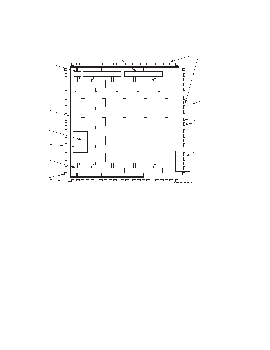
Figure 1. Series 4 Top Level Diagram
Programmable Logic Cells
The PLCs are arranged in an array of rows and columns. The location of a PLC is indicated by its row and column
so that a PLC in the second row and the third column is R2C3. The array of actual PLCs for every device begins
with R3C2 in all Series 4 generic FPGAs. PIOs are located on all four sides of the FPGA. Every group of four PIOs
on the device edge have an associated PIC.
The PLC consists of a PFU, SLIC, and routing resources. Each PFU within a PLC contains eight
4-input (16-bit) LUTs, eight latches/FFs, and one additional FF that may be used independently or with arithmetic
functions. The PFU is the main logic element of the PLC, containing elements for both combinatorial and sequential
logic. Combinatorial logic is done in LUTs located in the PFU. The PFU can be used in different modes to meet dif-
ferent logic requirements. The LUTs twin-quad architecture provides a configurable medium-/large-grain architec-
ture that can be used to implement from one to eight independent combinatorial logic functions or a large number
of complex logic functions using multiple LUTs. The flexibility of the LUT to handle wide input functions, as well as
multiple smaller input functions, maximizes the gate count per PFU while increasing system speed.
The PFU is organized in a twin-quad fashion: two sets of four LUTs and FFs that can be controlled independently.
Each PFU has two independent programmable clocks, clock enables, local set/reset, and data selects.
LUTs may also be combined for use in arithmetic functions using fast-carry chain logic in either 4-bit or 8-bit
modes. The carry-out of either mode may be registered in the ninth FF for pipelining. Each PFU may also be con-
figured as a synchronous 32x4 single- or dual-port RAM or ROM. The FFs (or latches) may obtain input from LUT
outputs or directly from invertible PFU inputs, or they can be tied high or tied low. The FFs also have programmable
clock polarity, clock enables, and local set/reset.
EMBEDDED
SYSTEM BUS
PIC
PLC
MICROPROCESSOR
INTERFACE (MPI)
PFU
SLIC
FPGA/SYSTEM
BUS INTERFACE
PLLs
EMBEDDED
BLOCK RAM
HIGH-SPEED I/Os
CLOCK PINS
PIO
REPLACED BY
EMBEDDED IP
CORE FOR FPSCs
(ALL 4 SIDES)
(ALL 4
CORNERS)

Lattice Semiconductor
7
Data Sheet
March, 2003
ORCA
Series 4 FPGAs
Programmable Logic Cells
(continued)
The LUTs can be programmed to operate in one of
three modes: combinatorial, ripple, or memory. In com-
binatorial mode, the LUTs can realize any 4-, 5-, or
6-input logic function and many multilevel logic func-
tions using
ORCA
's SWL connections. In ripple mode,
the high-speed carry logic is used for arithmetic func-
tions, comparator functions, or enhanced data path
functions. In memory mode, the LUTs can be used as a
32x4 synchronous read/write or ROM, in either single-
or dual-port mode.
The SLIC is connected from PLC routing resources
and from the outputs of the PFU. It contains eight
3-state, bidirectional buffers and logic to perform up to
a 10-bit AND function for decoding, or an AND-OR with
optional INVERT to perform
PAL
-like functions. The
3-state drivers in the SLIC and their direct connections
from the PFU outputs make fast, True 3-state buses
possible within the FPGA.
Programmable Function Unit
The PFUs are used for logic. Each PFU has 53 exter-
nal inputs and 20 outputs and can operate in several
modes. The functionality of the inputs and outputs
depends on the operating mode.
The PFU uses 36 data input lines for the LUTs, eight
data input lines for the latches/FFs, eight control inputs
(CLK[1:0], CE[1:0], LSR[1:0], SEL[1:0]), and a carry
input (CIN) for fast arithmetic functions and general-
purpose data input for the ninth FF. There are eight
combinatorial data outputs (one from each LUT), eight
latched/registered outputs (one from each latch/FF), a
carry-out (COUT), and a registered carry-out (REG-
COUT) that comes from the ninth FF. The carry-out sig-
nals are used principally for fast arithmetic functions.
There are also two dedicated F6 mode outputs which
are for the 6-input LUT function and 8 to 1 MUX.
Figure 2 and Figure 3 show high-level and detailed
views of the ports in the PFU, respectively. The eight
sets of LUT inputs are labeled as K0 through K7 with
each of the four inputs to each LUT having a suffix
of _x, where x is a number from 0 to 3.
There are four F5 inputs labeled A through D. These
are used for additional LUT inputs for 5- and 6-input
LUTs or as a selector for multiplexing two 4-input LUTs.
Four adjacent LUT4s can also be multiplexed together
with a 4 to 1 MUX to create a 6-input LUT. The eight
direct data inputs to the latches/FFs are labeled as
DIN[7:0]. Registered LUT outputs are shown as Q[7:0],
and combinatorial LUT outputs are labeled as F[7:0].
The PFU implements combinatorial logic in the LUTs
and sequential logic in the latches/FFs. The LUTs are
static random access memory (SRAM) and can be
used for read/write or ROM.
Each latch/FF can accept data from its associated LUT.
Alternatively, the latches/FFs can accept direct data
from DIN[7:0], eliminating the LUT delay if no combina-
torial function is needed. Additionally, the CIN input can
be used as a direct data source for the ninth FF. The
LUT outputs can bypass the latches/FFs, which
reduces the delay out of the PFU. It is possible to use
the LUTs and latches/FFs more or less independently,
allowing, for instance, a comparator function in the
LUTs simultaneously with a shift register in the FFs.
8
Lattice Semiconductor
Data Sheet
March, 2003
ORCA
Series 4 FPGAs
Programmable Logic Cells
(continued)
5-5752(F)a
Figure 2. PFU Ports
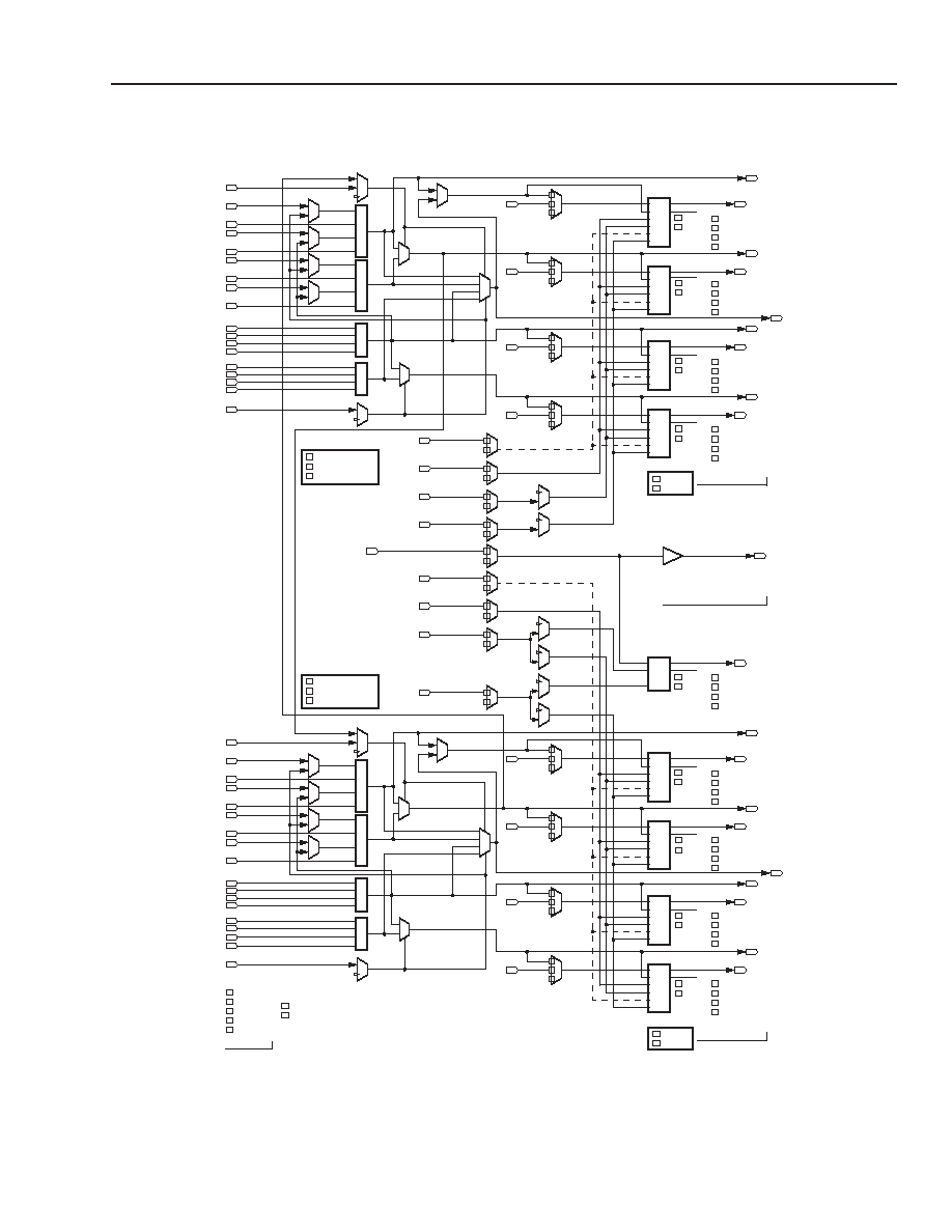
The PFU can be configured to operate in four modes: logic mode, half-logic mode, ripple mode, and memory
(RAM/ROM) mode. In addition, ripple mode has four submodes and RAM mode can be used in either a single- or
dual-port memory fashion. These submodes of operation are discussed in the following sections.
F5D
K7_0
K7_1
K7_2
K7_3
K6_0
K6_1
K6_2
K6_3
K5_0
K5_1
K5_2
K5_3
K4_0
K4_1
K4_2
K4_3
F5C
DIN7
DIN6
DIN5
DIN4
DIN3
DIN2
DIN1
DIN0
CIN
F5B
K3_0
K3_1
K3_2
K3_3
K2_0
K2_1
K2_2
K2_3
K1_0
K1_1
K1_2
K1_3
K0_0
K0_1
K0_2
K0_3
F5A
PROGRAMMABLE
FUNCTION UNIT
(PFU)
Q7
Q6
Q5
Q4
Q3
Q2
Q1
Q0
COUT
REGCOUT
F7
F6
F5
F4
F3
F2
F1
F0
SEL[0:1]
CE[0:1]
CLK[0:1]
LSR[0:1]
LUT603
LUT647
Lattice Semiconductor
9
Data Sheet
March, 2003
ORCA
Series 4 FPGAs
Programmable Logic Cells
(continued)
5-9714(F)
Note: All multiplexers without select inputs are configuration selector multiplexers.
Figure 3. Simplified PFU Diagram
K3_0MUX
K7_0MUX
D0
D1
SD
SP
CK
LSR
REG7
RESET
SET
Q7
F7
0
DIN7
DIN7MUX
D0
D1
SD
SP
CK
LSR
REG6
RESET
SET
Q6
F6
0
DIN6
DIN6MUX
D0
D1
SD
SP
CK
LSR
REG5
RESET
SET
Q5
F5
0
DIN5
DIN5MUX
D0
D1
SD
SP
CK
LSR
REG4
RESET
SET
Q4
F4
0
DIN4
DIN4MUX
LUT647
0
A
B
C
D
A
B
C
D
A
B
C
D
A
B
C
D
FSDMUX
K7_2MUX
K6_0MUX
K6_2MUX
AMUX
H7H6MUX
K7
K6
K5
K4
FSCMUX
H5H4MUX
LUT6MUX
F5D
K7_0
K7_1
K7_2
K7_3
K6_0
K6_1
K6_2
K6_3
K5_0
K5_1
K5_2
K5_3
K4_0
K4_1
K4_2
F5C
K4_3
D0
D1
SD
SP
CK
LSR
REG3
RESET
SET
Q3
F3
0
DIN3
DIN3MUX
D0
D1
SD
SP
CK
LSR
REG2
RESET
SET
Q2
F2
0
DIN2
DIN2MUX
D0
D1
SD
SP
CK
LSR
REG1
RESET
SET
Q1
F1
0
DIN1
DIN1MUX
D0
D1
SD
SP
CK
LSR
REG0
RESET
SET
DEL0
DEL1
DEL2
Q0
F0
0
DIN0
DIN0MUX
LUT603
0
A
B
C
D
A
B
C
D
A
B
C
D
A
B
C
D
FSBMUX
K3_2MUX
K2_0MUX
K2_2MUX
BMUX
H3H2MUX
K3
K2
K1
K0
F5AMUX
H1H0MUX
LUT6MUX
F5B
K3_0
K3_1
K3_2
K3_3
K2_0
K2_1
K2_2
K2_3
K1_0
K1_1
K1_2
K1_3
K0_0
K0_1
K0_2
F5A
K0_3
0
CLK1
CLK1MUX
0
SEL1
SEL1MUX
1
CE1
CE1MUX
CE47MUX
0
LSR1
LSR1MUX
LSR47MUX
0
CIN
1
0
0
CLK0
CLK0MUX
0
SEL0
SEL0MUX
1
CE0
CE0MUX
CEBMUX
0
LSR0
LSR0MUX
CE03MUX
1
0
LSRBMUX
LSR03MUX
1
0
D0
SP
CK
LSR
REG8
RESET
SET
RECCOUT
COUT
SR1MODEATTR
SR1MODE
CE1_OVER_LSR1
LSR1_OVER_CE1
RSYNC1
SR0MODEATTR
SR0MODE
CE0_OVER_LSR0
LSR0_OVER_CE0
ASYNC0
REGMODE_TOP
FF
LATCH
REG 4 THROUGH 7
THIS IS ALWAYS A FLIPFLOP
REGMODE_BOT
FF
LATCH
REG 0 THROUGH 3
LOGIC
MLOGIC
RIPPLE
RAM
ROM
ENABLED
DISABLED
GSR
PFU MODES
CINMUX
0
0
DEL3
DEL0
DEL1
DEL2
DEL3
DEL0
DEL1
DEL2
DEL3
DEL0
DEL1
DEL2
DEL3
DEL0
DEL1
DEL2
DEL3
DEL0
DEL1
DEL2
DEL3
DEL0
DEL1
DEL2
DEL3
DEL0
DEL1
DEL2
DEL3
DEL0
DEL1
DEL2
DEL3
10
Lattice Semiconductor
Data Sheet
March, 2003
ORCA
Series 4 FPGAs
Programmable Logic Cells
(continued)
Look-Up Table Operating Modes
The operating mode affects the functionality of the PFU input and output ports and internal PFU routing. For exam-
ple, in some operating modes, the DIN[7:0] inputs are direct data inputs to the PFU latches/FFs. In memory mode,
the same DIN[7:0] inputs are used as a 4-bit write data input bus and a 4-bit write address input bus into LUT
memory.
Table 2 lists the basic operating modes of the LUT. Figure 4--Figure 7 show block diagrams of the LUT operating
modes. The accompanying descriptions demonstrate each mode's use for generating logic.
Table 2. Look-Up Table Operating Modes
PFU Control Inputs
Each PFU has eight routable control inputs and an active-low, asynchronous global set/reset (GSRN) signal that
affects all latches and FFs in the device. The eight control inputs are CLK[1:0], LSR[1:0], CE[1:0], and SEL[1:0],
and their functionality for each logic mode of the PFU is shown in Table 3. The clock signal to the PFU is CLK, CE
stands for clock enable, which is its primary function. LSR is the local set/reset signal that can be configured as
synchronous or asynchronous. The selection of set or reset is made for each latch/FF and is not a function of the
signal itself. SEL is used to dynamically select between direct PFU input and LUT output data as the input to
the latches/FFs.
All of the control signals can be disabled and/or inverted via the configuration logic. A disabled clock enable
indicates that the clock is always enabled. A disabled LSR indicates that the latch/FF never sets/resets (except
from GSRN). A disabled SEL input indicates that DIN[7:0] PFU inputs are routed to the latches/FFs.
Table 3. Control Input Functionality
Mode
Function
Logic
4-, 5-, and 6-input LUTs; softwired LUTs; latches/FFs with direct input or LUT input; CIN as direct
input to ninth FF or as pass through to COUT.
Half Logic/
Half Ripple
Upper four LUTs and latches/FFs in logic mode; lower four LUTs and latches/FFs in ripple mode;
CIN and ninth FF for logic or ripple functions.
Ripple
All LUTs combined to perform ripple-through data functions. Eight LUT registers available for
direct-in use or to register ripple output. Ninth FF dedicated to ripple out, if used. The submodes of
ripple mode are adder/subtractor, counter, multiplier, and comparator.
Memory
All LUTs and latches/FFs used to create a 32x4 synchronous dual-port RAM. Can be used as
single-port or as ROM.
Mode
CLK
[1:0]
LSR
[1:0]
CE
[1:0]
SEL
[1:0]
Logic
CLK to all latches/
FFs
LSR to all latches/FFs,
enabled per nibble and
for ninth FF
CE to all latches/FFs,
selectable per nibble
and for ninth FF
Select between LUT
input and direct input for
eight latches/FFs
Half Logic/
Half Ripple
CLK to all latches/
FFs
LSR to all latches/FF,
enabled per nibble and
for ninth FF
CE to all latches/FFs,
selectable per nibble
and for ninth FF
Select between LUT
input and direct input for
eight latches/FFs
Ripple
CLK to all latches/
FFs
LSR to all latches/FFs,
enabled per nibble and
for ninth FF
CE to all latches/FFs,
selectable per nibble
and for ninth FF
Select between LUT
input and direct input for
eight latches/FFs
Memory
(RAM)
CLK to RAM
LSR0 Port enable 2
CE1 RAM write enable
CE0 Port enable 1
Not used
Memory
(ROM)
Optional for
synchronous outputs
Not used
Not used
Not used
Lattice Semiconductor
11
Data Sheet
March, 2003
ORCA
Series 4 FPGAs
Programmable Logic Cells
(continued)
Logic Mode
The PFU diagram of Figure 3 represents the logic
mode of operation. In logic mode, the eight LUTs are
used individually or in flexible groups to implement user
logic functions. The latches/FFs may be used in con-
junction with the LUTs or separately with the direct
PFU data inputs. There are three basic submodes of
LUT operation in PFU logic mode: F4 mode, F5 mode,
and the F6 mode. Combinations of the submodes are
possible in each PFU.
F4 mode, shown simplified in Figure 4, illustrates the
uses of the basic 4-input LUTs in the PFU. The output
of an F4 LUT can be passed out of the PFU, captured
at the LUTs associated latch/FF, or multiplexed with the
adjacent F4 LUT output using one of the F5[A:D] inputs
to the PFU. Only adjacent LUT pairs (K
0
and K
1
, K
2
and K
3
, K
4
and K
5
, K
6
and K
7
) can be multiplexed, and
the output always goes to the even-numbered output of
the pair.
The F5 submode of the LUT operation, shown simpli-
fied in Figure 4, indicates the use of 5-input LUTs to
implement logic. 5-input LUTs are created from two
4-input LUTs and a multiplexer. The F5 LUT is the
same as the multiplexing of two F4 LUTs described
previously with the constraint that the inputs to the F4
LUTs be the same. The F5[A:D] input is then used as
the fifth LUT input. The equations for the two F4 LUTs
will differ by the assumed value for the F5[A:D] input,
one F4 LUT assuming that the F5[A:D] input is zero,
and the other assuming it is a one. The selection of the
appropriate F4 LUT output in the F5 MUX by the
F5[A:D] signal creates a 5-input LUT. Any combination
of F4 and F5 LUTs is allowed per PFU using the eight
16-bit LUTs. Examples are eight F4 LUTs, four F5
LUTs, and a combination of four F4 plus two F5 LUTs.
Two 6-input LUTs are created by shorting together the
input of four 4-input LUTs (K0:3 and K4:7) which are
multiplexed together. The F5 inputs of the adjacent F4
LUTs derive the fifth and sixth inputs of the F6 mode.
The F6 outputs, LUT603 and LUT647, are dedicated to
the F6 mode or can be used as the outputs of
MUX8x1. MUX8x1 modes are created by programming
adjacent 4-input LUTs to 2x1 MUXs and multiplexing
down to create MUX8x1. Both F6 mode and MUX8x1
are available in the upper and lower PFU nibbles.
5-9733(F)
Figure 4. Simplified F4 and F5 Logic Modes
K7_0
K7_1
K7_2
F5D
LUT4
LUT4
2x1
MUX
F6
K7_3
K6_0
K6_1
K6_2
K6_3
K5_0
K5_1
K5_2
F5C
LUT4
LUT4
2x1
MUX
F4
K5_3
K4_0
K4_1
K4_2
K4_3
K3_0
K3_1
K3_2
F5B
LUT4
LUT4
2x1
MUX
F2
K3_3
K2_0
K2_1
K2_2
K2_3
K1_0
K1_1
K1_2
F5A
LUT4
LUT4
2x1
MUX
F0
K1_3
K0_0
K0_1
K0_2
K0_3
K7
F7
K6
F6
K5
F5
K4
F4
K3
F3
K2
F2
K1
F1
K0
F0
12
12
Lattice Semiconductor
Data Sheet
March, 2003
ORCA
Series 4 FPGAs
Programmable Logic Cells
(continued)
5-9734(F)a
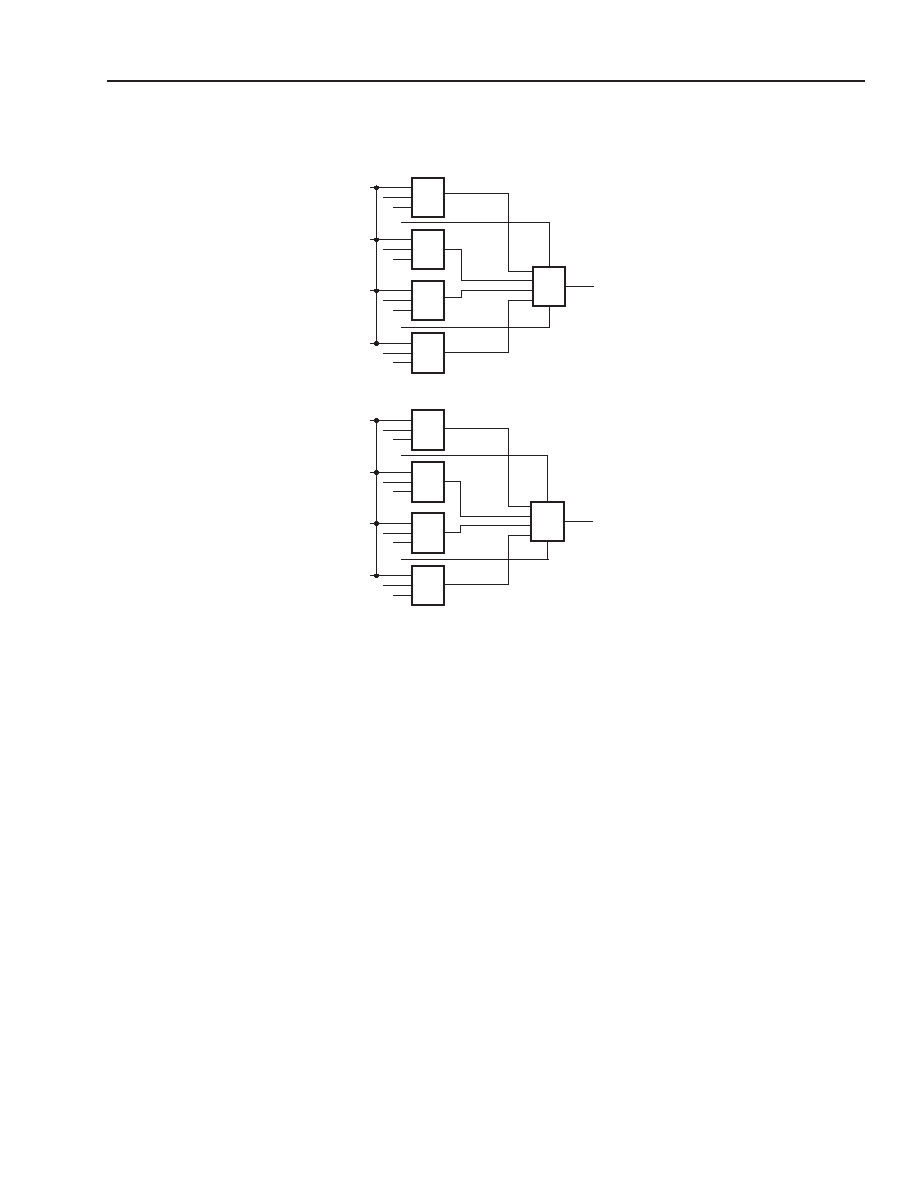
Figure 5. Simplified F6 Logic Modes
5-9735(F)
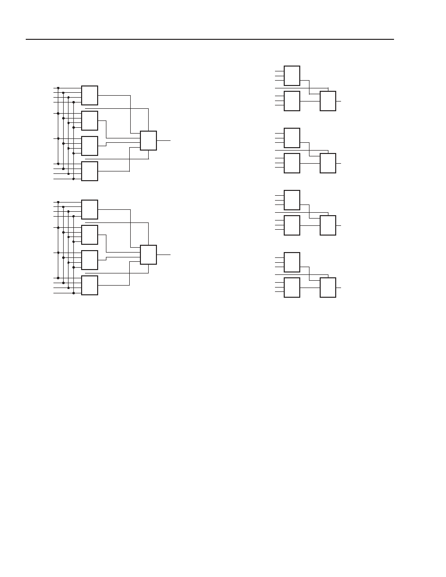
Figure 6. MUX 4x1
K7_0
K7_1
K7_2
K7_3
K6_0
K6_1
K6_2
K6_3
K5_0
K5_1
K5_2
K5_3
K4_0
K4_1
K4_2
K4_3
F5D
F5C
LUT4
LUT4
LUT4
LUT4
4x1
MUX
K3_0
K3_1
K3_2
K3_3
K2_0
K2_1
K2_2
K2_3
K1_0
K1_1
K1_2
K1_3
K0_0
K0_1
K0_2
K0_3
F5B
F5A
LUT4
LUT4
LUT4
LUT4
LUT603
4x1
MUX
LUT647
K7_0
K7_1
K7_2
F5D
LUT4
LUT4
2x1
MUX
K6_0
K6_1
K6_2
F4
K5_0
K5_1
K5_2
F5C
LUT4
LUT4
2x1
MUX
K4_0
K4_1
K4_2
F3
K3_0
K3_1
K3_2
F5B
LUT4
LUT4
2x1
MUX
K2_0
K2_1
K2_2
F2
K1_0
K1_1
K1_2
F5A
LUT4
LUT4
2x1
MUX
K0_0
K0_1
K0_2
F0
Lattice Semiconductor
13
Data Sheet
March, 2003
ORCA
Series 4 FPGAs
Programmable Logic Cells
(continued)
5-9736(F)a
Figure 7. MUX 8x1
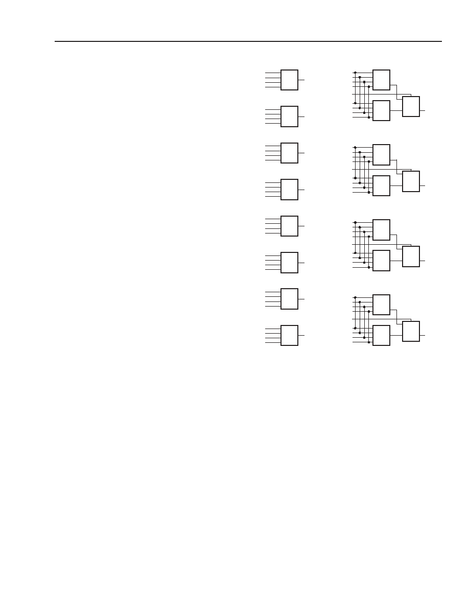
Softwired LUT submode uses F4, F5 and F6 LUTs and internal PFU feedback routing to generate complex logic
functions up to three LUT-levels deep. Multiplexers can be independently configured to route certain LUT outputs to
the input of other LUTs. In this manner, very complex logic functions, some of up to 22 inputs, can be implemented
in a single PFU at greatly enhanced speeds.
It is important to note that an LUT output that is fed back for softwired use is still available to be registered or output
from the PFU. This means, for instance, that a logic equation that is needed by itself and as a term in a larger equa-
tion need only be generated once, and PLC routing resources will not be required to use it in the larger equation.
K7_0
K7_1
K7_2
F5D
LUT4
LUT4
K6_0
K6_1
K6_2
LUT4
LUT4
K5_0
K5_1
K5_2
K4_0
K4_1
K4_2
F5C
LUT4
K3_0
K3_1
K3_2
F5B
LUT4
LUT4
K2_0
K2_1
K2_2
LUT4
LUT4
K1_0
K1_1
K1_2
K0_0
K0_1
K0_2
F5A
LUT4
MUX8x1
4x1
MUX
4x1
MUX
[LUT647]
MUX8x1
[LUT603]
14
Lattice Semiconductor
Data Sheet
March, 2003
ORCA
Series 4 FPGAs
Programmable Logic Cells
(continued)
5-5753(F)
5-5754(F)
Figure 8. Softwired LUT Topology Examples
F4
F4
F4
F4
F4
F4
F4
F4
FOUR 7-INPUT FUNCTIONS IN ONE PFU
F5
F5
F5
F5
TWO 9-INPUT FUNCTIONS IN ONE PFU
F5
F5
F5
F5
ONE 17-INPUT FUNCTION IN ONE PFU
F5
F5
F4
ONE 21-INPUT FUNCTION IN ONE PFU
F4
F4
F4
F4
F4
F4
F4
TWO 10-INPUT FUNCTIONS IN ONE PFU
F4
F4
F4
F4
3
ONE OF TWO 21-INPUT FUNCTIONS IN ONE PFU
ONE 22-INPUT FUNCTION IN ONE PFU
F5
F6
F4
F4
F4
F4
F4
F5
4-INPUT LUT
5-INPUT LUT
F6
6-INPUT LUT
Lattice Semiconductor
15
Data Sheet
March, 2003
ORCA
Series 4 FPGAs
Programmable Logic Cells
(continued)
Half-Logic Mode
Series 4 FPGAs are based upon a twin-quad architec-
ture in the PFUs. The byte-wide nature (eight LUTs,
eight latches/FFs) may just as easily be viewed as two
nibbles (two sets of four LUTs, four latches/FFs). The
two nibbles of the PFU are organized so that any nib-
ble-wide feature (excluding some softwired LUT topolo-
gies) can be swapped with any other nibble-wide
feature in another PFU. This provides for very flexible
use of logic and for extremely flexible routing. The half-
logic mode of the PFU takes advantage of the twin-
quad architecture and allows half of a PFU, K
[7:4]
and
associated latches/FFs, to be used in logic mode while
the other half of the PFU, K
[3:0]
and associated
latches/FFs, is used in ripple mode. In half-logic mode,
the ninth FF may be used as a general-purpose FF or
as a register in the ripple mode carry chain.
Ripple Mode
The PFU LUTs can be combined to do byte-wide ripple
functions with high-speed carry logic. Each LUT has a
dedicated carry-out net to route the carry to/from any
adjacent LUT. Using the internal carry circuits, fast
arithmetic, counter, and comparison functions can be
implemented in one PFU. Similarly, each PFU has
carry-in (CIN, FCIN) and carry-out (COUT, FCOUT)
ports for fast-carry routing between adjacent PFUs.
The ripple mode is generally used in operations on two
data buses. A single PFU can support an 8-bit ripple
function. Data buses of 4 bits and less can use the
nibble-wide ripple chain that is available in half-logic
mode. This nibble-wide ripple chain is also useful for
longer ripple chains where the length modulo 8 is four
or less. For example, a 12-bit adder (12 modulo 8 = 4)
can be implemented in one PFU in ripple mode (8 bits)
and one PFU in half-logic mode (4 bits), freeing half of
a PFU for general logic mode functions.
Each LUT has two operands and a ripple (generally
carry) input, and provides a result and ripple (generally
carry) output. A single bit is rippled from the previous
LUT and is used as input into the current LUT. For LUT
K
0
, the ripple input is from the PFU CIN or FCIN port.
The CIN/FCIN data can come from either the fast-carry
routing (FCIN) or the PFU input (CIN), or it can be tied
to logic 1 or logic 0.
In the following discussions, the notations LUT K
7
/K
3
and F[7:0]/F[3:0]
are used to denote the LUT that pro-
vides the carry-out and the data outputs for full PFU
ripple operation (K
7
, F[7:0]) and half-logic ripple
operation (K
3
, F[3:0]), respectively. The ripple mode
diagram (Figure 9) shows full PFU ripple operation,
with half-logic ripple connections shown as dashed
lines.
The result output and ripple output are calculated by
using generate/propagate circuitry. In ripple mode, the
two operands are input into K
Z
[1] and K
Z
[0] of each
LUT. The result bits, one per LUT, are F[7:0]/F[3:0]
(see
Figure 9). The ripple output from LUT K
7
/K
3
can be
routed on dedicated carry circuitry into any of four adja-
cent PLCs, and it can be placed on the PFU COUT/
FCOUT outputs. This allows the PLCs to be cascaded
in the ripple mode so that nibble-wide ripple functions
can be expanded easily to any length.
Result outputs and the carry-out may optionally be reg-
istered within the PFU. The capability to register the
ripple results, including the carry output, provides for
improved counter performance and simplified pipelin-
ing in arithmetic functions.
5-5755(F).
Figure 9. Ripple Mode
F7
K
7
[1]
K
7
[0]
K7
D
Q
C
C
D
Q
Q7
REGOUT
COUT
F6
K
6
[1]
K
6
[0]
K6
D
Q
Q6
F4
K
4
[1]
K
4
[0]
K4
D
Q
Q4
F3
K
3
[1]
K
3
[0]
K3
D
Q
Q3
F2
K
2
[1]
K
2
[0]
K2
D
Q
Q2
F1
K
1
[1]
K
1
[0]
K1
D
Q
Q1
F5
K
5
[1]
K
5
[0]
K5
D
Q
Q5
F0
K
0
[1]
K
0
[0]
K0
D
Q
Q0
CIN/FCIN
FCOUT

16
16
Lattice Semiconductor
Data Sheet
March, 2003
ORCA
Series 4 FPGAs
Programmable Logic Cells
(continued)
The ripple mode can be used in one of four submodes.
The first of these is adder-subtractor submode. In
this submode, each LUT generates three separate out-
puts. One of the three outputs selects whether the
carry-in is to be propagated to the carry-out of the cur-
rent LUT or if the carry-out needs to be generated. If
the carry-out needs to be generated, this is provided by
the second LUT output. The result of this selection is
placed on the carry-out signal, which is connected to
the next LUT carry-in or the COUT/FCOUT signal, if it
is the last LUT (K
7
/K
3
). Both of these outputs can be
any equation created from K
Z
[1] and K
Z
[0], but in this
case, they have been set to the propagate and gener-
ate functions.
The third LUT output creates the result bit for each LUT
output connected to F[7:0]/F[3:0]. If an adder/subtrac-
tor is needed, the control signal to select addition or
subtraction is input on F5A/F5C inputs. These inputs
generate the controller input AS. When AS = 0 this
function performs the adder, A + B. When AS = 1 the
function performs the subtractor, A � B. The result bit is
created in one-half of the LUT from a single bit from
each input bus K
Z
[1:0], along with the ripple input bit.
The second submode is the counter submode (see
Figure 10). The present count, which may be initialized
via the PFU DIN inputs to the latches/FFs, is supplied
to input K
Z
[0], and then output F[7:0]/F[3:0] will either
be incremented by one for an up counter or decre-
mented by one for a down counter. If an up/down
counter is needed, the control signal to select the direc-
tion (up or down) is input on F5A and F5C. When
F5[A:C], respectively per nibble, is a logic 1, this indi-
cates a down counter and a logic 0 indicates an up
counter.
5-5756(F)
Figure 10. Counter Submode
F7
K
7
[0]
K7
D
Q
C
C
D
Q
Q7
REGCOUT
COUT
F6
K
6
[0]
K6
D
Q
Q6
F4
K
4
[0]
K4
D
Q
Q4
F3
K
3
[0]
K3
D
Q
Q3
F2
K
2
[0]
K2
D
Q
Q2
F1
K
1
[0]
K1
D
Q
Q1
F5
K
5
[0]
K5
D
Q
Q5
F0
K
0
[0]
K0
D
Q
Q0
CIN/FCIN
FCOUT
Lattice Semiconductor
17
Data Sheet
March, 2003
ORCA
Series 4 FPGAs
Programmable Logic Cells
(continued)
In the third submode, multiplier submode, a single
PFU can affect an 8x1 bit (4x1 for half-ripple mode)
multiply and sum with a partial product (see Figure 11).
The multiplier bit is input at F5[A:C], respectively per
nibble, and the multiplicand bits are input at K
Z
[1],
where K
7
[1] is the most significant bit (MSB). K
Z
[0] con-
tains the partial product (or other input to be summed)
from a previous stage. If F5[A:C] is logical 1, the multi-
plicand is added to the partial product. If F5[A:C] is log-
ical 0, 0 is added to the partial product, which is the
same as passing the partial product. CIN/FCIN can
bring the carry-in from the less significant PFUs if the
multiplicand is wider than 8 bits, and COUT/FCOUT
holds any carry-out from the multiplication, which may
then be used as part of the product or routed to another
PFU in multiplier mode for multiplicand width expan-
sion.
Ripple mode's fourth submode features equality
comparators. The functions that are explicitly available
are A
B, A
B, and A
B, where the value for A is
input on K
Z
[0], and the value for B is input on K
Z
[1]. A
value of 1 on the carry-out signals valid argument. For
example, a carry-out equal to 1 in AB submode indi-
cates that the value on K
Z
[0] is greater than or equal to
the value on K
Z
[1]. Conversely, the functions A
B,
A + B, and A > B are available using the same func-
tions but with a 0 output expected. For example, A
>
B
with a 0 output indicates A
B. Table 4 shows each
function and the output expected.
If larger than 8 bits, the carry-out signal can be cas-
caded using fast-carry logic to the carry-in of any adja-
cent PFU. The use of this submode could be shown
using Figure 9, except that the CIN/FCIN input for the
least significant PFU is controlled via configuration.
Table 4. Ripple Mode Equality Comparator
Functions and Outputs
5-5757(F)
Key: C = configuration data.
Note: F5[A:C] shorted together
Figure 11. Multiplier Submode
Equality
Function
ispLEVER
Submode
True, if
Carry-Out Is:
A
B
A
B
1
A
B
A
B
1
A
B
A
B
1
A < B
A
B
0
A > B
A
B
0
A = B
A
B
0
K7[1]
K7[0]
+
D
Q
C
C
D Q
1
0
0
K7
F5[A:C]
K4[1]
K4[0]
+
D
Q
1
0
0
K4
K3[1]
K3[0]
+
D
Q
1
0
0
K3
K2[1]
K2[0]
+
D
Q
1
0
0
K2
K1[1]
K1[0]
+
D
Q
1
0
0
K1
K6[1]
K6[0]
+
D
Q
1
0
0
K6
K5[1]
K5[0]
+
D
Q
1
0
0
K5
K0[1]
K0[0]
+
D
Q
1
0
0
K0
Q0
F0
Q1
F1
Q2
F2
Q3
F3
Q4
F4
Q5
F5
Q6
F6
Q7
F7
COUT
REGCOUT
18
Lattice Semiconductor
Data Sheet
March, 2003
ORCA
Series 4 FPGAs
Programmable Logic Cells
(continued)
Memory Mode
The Series 4 PFU can be used to implement a 32x4 (128-bit) synchronous, dual-port RAM). A block diagram of a
PFU in memory mode is shown in Figure 12. This RAM can also be configured to work as a single-port memory
and because initial values can be loaded into the RAM during configuration, it can also be used as a ROM.
5-5969(F)a
1. CLK[0:1] are commonly connected in memory mode.
2. CE1 = write enable = wren; wren = 0 (no write enable); wren = 1 (write enabled).
CE0 = write port enable 0; CE0 = 0, wren = 0; CE0 = 1, wren = CE1.
LSR0 = write port enable 1; LSR0 = 0, wren = CE0; LSR0 = 1, wren = CE1.
Figure 12. Memory Mode
Q6
Q4
Q2
Q0
D
5
Q
CIN(WA1)
K
Z
[3:0]
4
F5[A:D]
D Q
DIN7(WA3)
D Q
DIN5(WA2)
D Q
DIN3(WA1)
D Q
DIN1(WA0)
D Q
DIN6(WD3)
D Q
DIN4(WD2)
D Q
DIN2(WD1)
D Q
DIN0(WD0)
D Q
CE0, LSR0
S/E
CLK[0:1]
4
WRITE
WRITE
READ
READ
4
F6
F4
F2
F0
D Q
D Q
D Q
D Q
WRITE
RAM CLOCK
ADDRESS[4:0]
ADDRESS[4:0]
DATA[3:0]
DATA[3:0]
ENABLE
(SEE NOTE 2.)
CE1

Lattice Semiconductor
19
Data Sheet
March, 2003
ORCA
Series 4 FPGAs
Programmable Logic Cells
(continued)
The PFU memory mode uses all LUTs and latches/FFs
including the ninth FF in its implementation as shown in
Figure 12. The read address is input at the K
Z
[3:0] and
F5[A:D] inputs where K
Z
[0] is the LSB and F5[A:D] is
the MSB, and the write address is input on CIN (MSB)
and DIN[7, 5, 3, 1], with DIN[1] being the LSB. Write
data is input on DIN[6, 4, 2, 0], where DIN[6] is the
MSB, and read data is available combinatorially on
F[6, 4, 2, 0] and registered on Q[6, 4, 2, 0] with F[6] and
Q[6] being the MSB. The write enable controlling ports
are input on CE0, CE1, and LSR0. CE1 is the active-
high write enable (CE1 = 1, RAM is write enabled). The
first write port is enabled by CE0. The second write
port is enabled with LSR0. The PFU CLK (CLK0) signal
is used to synchronously write the data. The polarities
of the clock, write enable, and port enables are all pro-
grammable. Write-port enables may be disabled if they
are not to be used.
Data is written to the write data, write address, and
write enable registers on the active edge of the clock,
but data is not written into the RAM until the next clock
edge one-half cycle later. The read port is actually
asynchronous, providing the user with read data very
quickly after setting the read address, but timing is also
provided so that the read port may be treated as fully
synchronous for write then read applications. If the
read and write address lines are tied together (main-
taining MSB to MSB, etc.), then the dual-port RAM
operates as a synchronous single-port RAM. If the
write enable is disabled, and an initial memory contents
is provided at configuration time, the memory acts as a
ROM (the write data and write address ports and write
port enables are not used).
Wider memories can be created by operating two or
more memory mode PFUs in parallel, all with the same
address and control signals, but each with a different
nibble of data. To increase memory word depth above
32, two or more PLCs can be used. Figure 10 shows a
128x8 dual-port RAM that is implemented in eight
PLCs. This figure demonstrates data path width expan-
sion by placing two memories in parallel to achieve an
8-bit data path. Depth expansion is applied to achieve
128 words deep using the 32-word deep PFU memo-
ries. In addition to the PFU in each PLC, the SLIC
(described in the next section) in each PLC is used for
read address decodes and 3-state drivers. The 128x8
RAM shown could be made to operate as a single-port
RAM by tying (bit-for-bit) the read and write addresses.
To achieve depth expansion, one or two of the write
address bits (generally the MSBs) are routed to the
write port enables as in Figure 10. For 2 bits, the bits
select which 32-word bank of RAM of the four available
from a decode of two WPE inputs is to be written. Simi-
larly, 2 bits of the read address are decoded in the
SLIC and are used to control the 3-state buffers
through which the read data passes. The write data bus
is common, with separate nibbles for width expansion,
across all PLCs, and the read data bus is common
(again, with separate nibbles) to all PLCs at the output
of the 3-state buffers.
Figure 13 also shows the capability to provide a read
enable for RAMs/ROMs using the SLIC cell. The read
enable will 3-state the read data bus when inactive,
allowing the write data and read data buses to be tied
together if desired.
20
Lattice Semiconductor
Data Sheet
March, 2003
ORCA
Series 4 FPGAs
Programmable Logic Cells
(continued)
5-5749(F)
Figure 13. Memory Mode Expansion Example--128x8 RAM
RD[7:0]
WE
WA[6:0]
RA[6:0]
CLK
WA
RA
WPE 1
WPE 2
WE
WD[7:4]
5
5
4
PLC
8
WD[7:0]
8
7
7
WA
RA
WPE 1
WPE 2
WE
RD[3:0]
WD[3:0]
5
5
4
PLC
RD[7:4]
WA
RA
WPE 1
WPE 2
WE
WD[7:4]
5
5
4
PLC
WA
RA
WPE 1
WPE 2
WE
RD[3:0]
WD[3:0]
5
5
4
PLC
RD[7:4]
RE
RE
4
RE
4
RE
4
RE
4
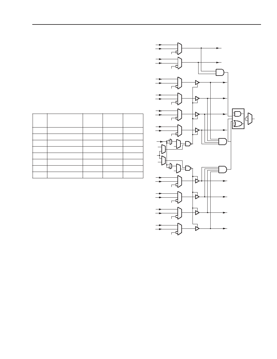
Supplemental Logic and Interconnect Cell
Each PLC contains a SLIC embedded within the PLC
routing, outside of the PFU. As its name indicates, the
SLIC performs both logic and interconnect (routing)
functions. Its main features are 3-statable, bidirectional
buffers, and a PAL-like decoder capability. Figure 14
shows a diagram of a SLIC with all of its features
shown. All modes of the SLIC are not available at one
time.
The ten SLIC inputs can be sourced directly from the
PFU or from the general routing fabric. SI[0:9] inputs
can come from the horizontal or vertical routing and
I[0:9} comes from the PFU outputs O[9:0]. These inputs
can also be tied to a logical 1 or 0 constant. The inputs
are twin-quad in nature and are segregated into two
groups of four nibbles and a third group of two inputs
for control. Each input nibble groups also have
3-state capability, however the third pair does not.
There is one 3-state control (TRI) for each SLIC, with
the capability to invert or disable the 3-state control for
each group of four BIDIs. Separate 3-state control for
each nibble-wide group is achievable by using the
SLICs decoder (DEC) output, driven by the group of
two BIDIs, to control the 3-state of one BIDI nibble
while using the TRI signal to control the 3-state of the
other BIDI nibble. Figure 15
shows the SLIC in buffer
mode with available 3-state control from the TRI and
DEC signals. If the entire SLIC is acting in a buffer
capacity, the DEC output may be used to generate a
constant logic 1 (V
HI
) or logic 0 (V
LO
) signal for general
use.
The SLIC may also be used to generate PAL-like AND-
OR with optional INVERT (AOI) functions or a decoder
of up to 10 bits. Each group of buffers can feed into an
AND gate (4-input AND for the nibble groups and
2-input AND for the other two buffers). These AND
gates then feed into a 3-input gate that can be config-
ured as either an AND gate or an OR gate. The output
of the 3-input gate is invertible and is output at the DEC
output of the SLIC. Figure 19 shows the SLIC in full
decoder mode.
The functionality of the SLIC is parsed by the two nib-
ble-wide groups and the 2-bit buffer group. Each of
these groups may operate independently as BIDI buff-
ers (with or without 3-state capability for the nibble-
wide groups) or as a PAL/decoder.
Lattice Semiconductor
21
Data Sheet
March, 2003
ORCA
Series 4 FPGAs
Programmable Logic Cells
(continued)
As discussed in the memory mode section, if the SLIC
is placed into one of the modes where it contains both
buffers and a decode or AOI function (e.g.,
BUF_BUF_DEC mode), the DEC output can be gated
with the 3-state input signal. This allows up to a 6-input
decode (e.g., BUF_DEC_DEC mode) plus the 3-state
input to control the enable/disable of up to four buffers
per SLIC Figure 15--Figure 19 show several configura-
tions of the SLIC, while Table 5 shows all of the possi-
ble modes.
Table 5. SLIC Modes
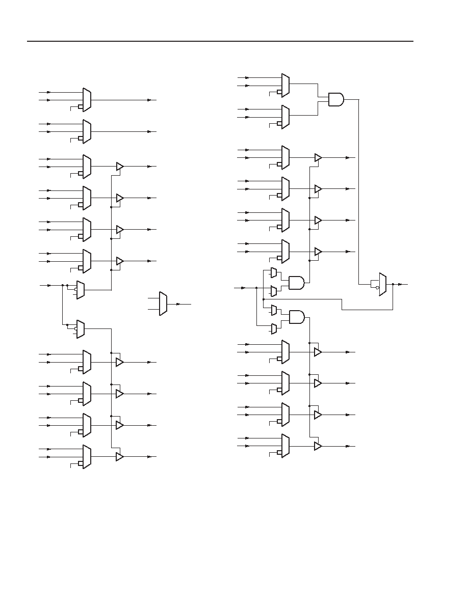
5-5744(F).a.
Figure 14. SLIC All Modes Diagram
Mode
No.
Mode
BUF
[3:0]
BUF
[7:4]
BUF
[9:8]
1
BUFFER
Buffer
Buffer
Buffer
2
BUF_BUF_DEC
Buffer
Buffer
Decoder
3
BUF_DEC_BUF
Buffer
Decoder
Buffer
4
BUF_DEC_DEC
Buffer
Decoder Decoder
5
DEC_BUF_BUF Decoder
Buffer
Buffer
6
DEC_BUF_DEC
Decoder
Buffer
Decoder
7
DEC_DEC_BUF
Decoder Decoder
Buffer
8
DECODER
Decoder Decoder Decoder
SIN9
I9
SOUT09
DEC
DEC
0/1
0/1
TRI
0/1
0/1
SOUT08
SOUT07
SOUT06
SOUT05
SOUT04
SOUT03
SOUT02
SOUT01
SOUT00
LOGIC 1 OR 0
SIN8
I8
LOGIC 1 OR 0
SIN7
I7
LOGIC 1 OR 0
SIN6
I6
LOGIC 1 OR 0
SIN5
I5
LOGIC 1 OR 0
SIN4
I4
LOGIC 1 OR 0
SIN3
I3
LOGIC 1 OR 0
SIN2
I2
LOGIC 1 OR 0
SIN1
I1
LOGIC 1 OR 0
SIN0
I0
LOGIC 1 OR 0
22
Lattice Semiconductor
Data Sheet
March, 2003
ORCA
Series 4 FPGAs
Programmable Logic Cells
(continued)
5-5745(F).a
Figure 15. Buffer Mode
5-5746(F).a
Figure 16. Buffer-Buffer-Decoder Mode
SOUT08
TRI
0/1
0/1
1
0
DEC
THIS CAN BE USED TO GENERATE
A VHI OR VLO
SIN8
I8
LOGIC 1 OR 0
SOUT09
SIN9
I9
LOGIC 1 OR 0
SOUT07
SIN7
I7
LOGIC 1 OR 0
SOUT06
SIN6
I6
LOGIC 1 OR 0
SOUT05
SIN5
I5
LOGIC 1 OR 0
SOUT04
SIN4
I4
LOGIC 1 OR 0
SOUT03
SIN3
I3
LOGIC 1 OR 0
SOUT02
SIN2
I2
LOGIC 1 OR 0
SOUT01
SIN1
I1
LOGIC 1 OR 0
SOUT00
SIN0
I0
LOGIC 1 OR 0
TRI
DEC
1
1
1
1
SOUT07
SIN7
I7
LOGIC 1 OR 0
SOUT06
SIN6
I6
LOGIC 1 OR 0
SOUT05
SIN5
I5
LOGIC 1 OR 0
SOUT04
SIN4
I4
LOGIC 1 OR 0
SIN9
I9
LOGIC 1 OR 0
SIN8
I8
LOGIC 1 OR 0
SOUT03
SIN3
I3
LOGIC 1 OR 0
SOUT02
SIN2
I2
LOGIC 1 OR 0
SOUT01
SIN1
I1
LOGIC 1 OR 0
SOUT00
SIN0
I0
LOGIC 1 OR 0

Lattice Semiconductor
23
Data Sheet
March, 2003
ORCA
Series 4 FPGAs
Programmable Logic Cells
(continued)
5-5747(F).a
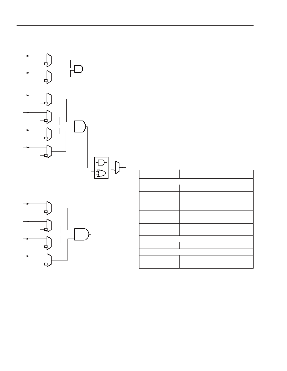
Figure 17. Buffer-Decoder-Buffer Mode
5-5750(F)
Figure 18. Buffer-Decoder-Decoder Mode
TRI
DEC
1
1
SOUT08
SIN8
I8
LOGIC 1 OR 0
SOUT09
SIN9
I9
LOGIC 1 OR 0
SIN7
LOGIC 1 OR 0
SIN6
LOGIC 1 OR 0
SIN5
LOGIC 1 OR 0
SIN4
LOGIC 1 OR 0
SOUT03
SIN3
I3
LOGIC 1 OR 0
SOUT02
SIN2
I2
LOGIC 1 OR 0
SOUT01
SIN1
I1
LOGIC 1 OR 0
SOUT00
SIN0
I0
LOGIC 1 OR 0
IF LOW THEN 3 STATE BUFFERS ARE HIGH Z
DEC
TRI
1
1
SIN7
LOGIC 1 OR 0
SIN6
LOGIC 1 OR 0
SIN5
LOGIC 1 OR 0
SIN4
LOGIC 1 OR 0
SOUT03
SIN3
I3
LOGIC 1 OR 0
SOUT02
SIN2
I2
LOGIC 1 OR 0
SOUT01
SIN1
I1
LOGIC 1 OR 0
SOUT00
SIN0
I0
LOGIC 1 OR 0
SIN9
LOGIC 1 OR 0
SIN8
LOGIC 1 OR 0
24
24
Lattice Semiconductor
Data Sheet
March, 2003
ORCA
Series 4 FPGAs
Programmable Logic Cells
(continued)
5-5748(F)
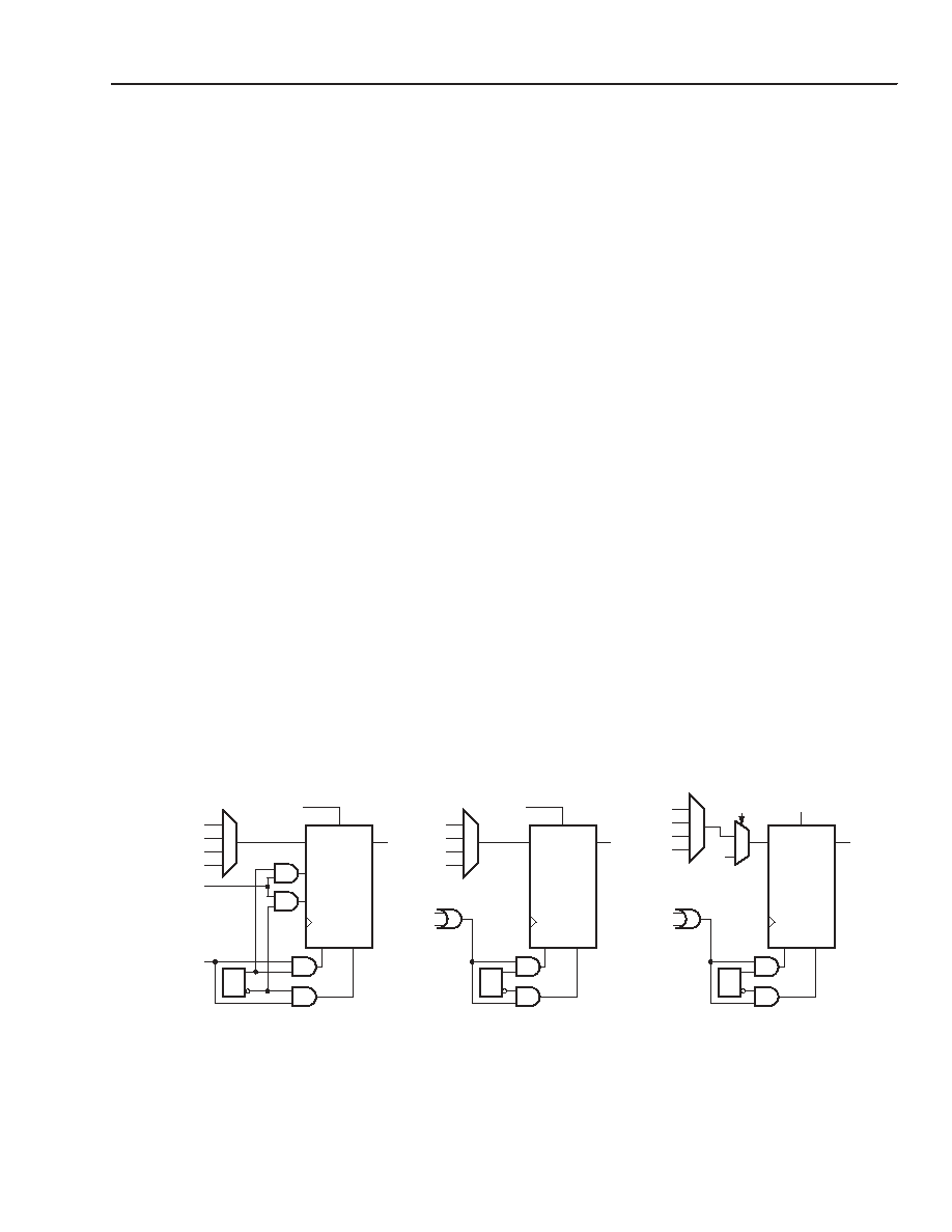
Figure 19. Decoder Mode
PLC Latches/Flip-Flops
The eight general-purpose latches/FFs in the PFU can
be used in a variety of configurations. In some cases,
the configuration options apply to all eight latches/FFs
in the PFU and some apply to the latches/FFs on a nib-
ble-wide basis where the ninth FF is considered inde-
pendently. For other options, each latch/FF is
independently programmable. In addition, the ninth FF
can be used for a variety of functions.
Table 6 summarizes these latch/FF options. The
latches/FFs can be configured as either positive- or
negative-level sensitive latches, or positive or negative
edge-triggered FFs (the ninth register can only be a
FF). All latches/FFs in a given PFU share the same
clock, and the clock to these latches/FFs can be
inverted. The input into each latch/FF is from either the
corresponding LUT output (F[7:0]) or the direct data
input (DIN[7:0]). The latch/FF input can also be tied to
logic 1 or to logic 0, which is the default.
Table 6. Configuration RAM Controlled Latch/
Flip-Flop Operation
Each PFU has two independent programmable clocks,
clock enable CE[1:0], local set/reset LSR[1:0], and
front end data selects SEL[1:0]. When CE is disabled,
each latch/FF retains its previous value when clocked.
The clock enable, LSR, and SEL inputs can be inverted
to be active-low.
DEC
SIN7
LOGIC 1 OR 0
SIN6
LOGIC 1 OR 0
SIN5
LOGIC 1 OR 0
SIN4
LOGIC 1 OR 0
SIN9
LOGIC 1 OR 0
SIN8
LOGIC 1 OR 0
SIN3
LOGIC 1 OR 0
SIN1
LOGIC 1 OR 0
SIN2
LOGIC 1 OR 0
SIN0
LOGIC 1 OR 0
Function Options
Common to All Latches/FFs in PFU
LSR Operation
Asynchronous or synchronous.
Clock Polarity
Noninverted or inverted.
Front-end Select* Direct (DIN[7:0]) or from LUT
(F[7:0]).
LSR Priority
Either LSR or CE has priority.
Latch/FF Mode
Latch or FF.
Enable GSRN
GSRN enabled or has no effect on
PFU latches/FFs.
Set Individually in Each Latch/FF in PFU
Set/Reset Mode
Set or reset.
By Group (Latch/FF[3:0], Latch/FF[7:4], and FF[8])
Clock Enable
CE or none.
LSR Control
LSR or none.
* Not available for FF[8].
Lattice Semiconductor
25
Data Sheet
March, 2003
ORCA
Series 4 FPGAs
Programmable Logic Cells
(continued)
The set/reset operation of the latch/FF is controlled by
two parameters: reset mode and set/reset value. When
the GSRN and local set/reset (LSR) signals are not
asserted, the latch/FF operates normally. The reset
mode is used to select a synchronous or asynchronous
LSR operation. If synchronous, LSR has the option to
be enabled only if clock enable (CE) is active or for LSR
to have priority over the clock enable input, thereby set-
ting/resetting the FF independent of the state of the
clock enable. The clock enable is supported on FFs, not
latches. It is implemented by using a 2-input multiplexer
on the FF input, with one input being the previous state
of the FF and the other input being the new data
applied to the FF. The select of this 2-input multiplexer
is clock enable (CE), which selects either the new data
or the previous state. When the clock enable is inactive,
the FF output does not change when the clock edge
arrives.
The GSRN signal is only asynchronous, and it sets/
resets all latches/FFs in the FPGA based upon the set/
reset configuration bit for each latch/FF. The set/reset
value determines whether GSRN and LSR are set or
reset inputs. The set/reset value is independent for
each latch/FF. An option is available to disable the
GSRN function per PFU after initial device configura-
tion.
The latch/FF can be configured to have a data front-
end select. Two data inputs are possible in the front-end
select mode, with the SEL signal used to select which
data input is used. The data input into each
latch/FF is from the output of its associated LUT,
F[7:0], or direct from DIN[7:0], bypassing the LUT. In
the front-end data select mode, both signals are avail-
able to the latches/FFs.
If either or both of these inputs is unused or is unavail-
able, the latch/FF data input can be tied to a logic 0 or
logic 1 instead (the default is logic 0).
The latches/FFs can be configured in three basic
modes:
Local synchronous set/reset: the input into the PFU's
LSR port is used to synchronously set or reset each
latch/FF.
Local asynchronous set/reset: the input into LSR
asynchronously sets or resets each latch/FF.
Latch/FF with front-end select, LSR either synchro-
nous or asynchronous: the data select signal selects
the input into the latches/FFs between the LUT out-
put and direct data in.
For all three modes, each latch/FF can be indepen-
dently programmed as either set or reset. Figure 20
provides the logic functionality of the front-end select,
global set/reset, and local set/reset operations.
The ninth PFU FF, which is generally associated with
registering the carry-out signal in ripple mode func-
tions, can be used as a general-purpose FF. It is only
an FF and is not capable of being configured as a
latch. Because the ninth FF is not associated with an
LUT, there is no front-end data select. The data input to
the ninth FF is limited to the CIN input, logic 1, logic 0,
or the carry-out in ripple and half-logic modes.
5-9737(F).a
Key: C = configuration data.
Figure 20. Latch/FF Set/Reset Configurations
CE
CE
D
Q
S_SET
S_RESET
CLK
SET RESET
F
DIN
LOGIC 1
LOGIC 0
LSR
CD
GSRN
CE
CE
D
Q
CLK
SET RESET
F
DIN
LOGIC 1
LOGIC 0
CD
GSRN
LSR
CE
CE
D
Q
CLK
SET RESET
F
DIN
LOGIC 1
LOGIC 0
CD
GSRN
LSR
DIN
SEL
26
26
Lattice Semiconductor
Data Sheet
March, 2003
ORCA
Series 4 FPGAs
Embedded Block RAM (EBR)
The ORCA Series 4 devices compliment the distributed
PFU RAM with large blocks of memory macrocells. The
memory is available in 512 words by 18 bits/word
blocks with 2 read and 2 write ports with two byte lane
enables which operate with quad-port functionality.
Additional logic has been incorporated for FIFO, multi-
plier, and CAM implementations. The RAM blocks are
organized along the PLC rows and are added in pro-
portion to the FPGA array sizes as shown in Table 7.
The contents of the RAM blocks may be optionally ini-
tialized during FPGA configuration.
Table 7. ORCA Series 4-- Available Embedded
Block RAM
Each highly flexible 512x18 (quad-port, two read/two
write) RAM block can be programmed by the user to
meet their particular function. Each of the EBR configu-
rations use the physical signals as shown in
Table 8. Quad-port addressing permits simultaneous
read and write operations on all four ports.
The EBR ports are written synchronously on the posi-
tive-edge of CKW. Synchronous read operations uses
the positive-edge of CKR. Options are available to use
synchronous read address registers and read output
registers, or to bypass these registers and have the
RAM read operate asynchronously. Detailed informa-
tion about the EBR blocks is found in various applica-
tion notes.
ispLEVER provides SCUBA as a RAM generation tool
for EBR RAMs. Many of the EBR sub-modes are sup-
ported and the initialization values can also be defined.
EBR Features
Quad Port RAM Modes (Two Read/Two Write)
One 512 x 18 RAM with optional built-in write arbitra-
tion.
One 1024 x 18 RAM built on two blocks with built-in
decode logic for simplified implementation.
Dual Port RAM Modes (One Read/One Write)
One 256 x 36 RAM.
One 1K x 9 RAM.
Two independent 512 x 9 RAMs built in one EBR with
separate read clocks, write clocks and enables.
Two independent RAMS with arbitrary number of
words whose sum is 512 words or less by 18 bits/
word or less.
The joining of RAM blocks is supported to create wider
deeper memories. The adjacent routing interface pro-
vided by the CIBs allow the cascading of blocks
together with minimal penalties due to routing delays.
It is also possible to connect any or all of the EBR RAM
blocks together through the embedded system bus,
which is discussed in a later section of this data sheet.
Arbitration logic is optionally programmed by the user
to signal occurrences of data collisions as well as to
block both ports from writing at the same time. The
arbitration logic prioritizes PORT1. When utilizing the
arbiter, the signal BUSY indicates data is being written
to PORT1. This BUSY output signals PORT1 activity by
driving a high output. If the arbiter is turned off both
ports could be written at the same time and the data
would be corrupt. In this scenario the BUSY signal will
indicate a possible error.
There is also a user option which dedicates PORT 1 to
communications to the system bus. In this mode the
user logic only has access to PORT0 and arbitration
logic is enabled. The system bus utilizes the priority
given to it by the arbiter therefore the system bus will
always be able to write to the EBR.
Device
Number of
Blocks
Number of
EBR Bits
OR4E02
8
74K
OR4E04
12
111K
OR4E06
16
147K

Lattice Semiconductor
27
Data Sheet
March, 2003
ORCA
Series 4 FPGAs
Embedded Block RAM (EBR)
(continued)
FIFO Modes
FIFOs can be configured to 256, 512, or 1K depths and
36, 18, or 9 widths respectively but also can be
expanded using multiple blocks. FIFO works synchro-
nously with the same read and write clock where the
read port can be registered on the output or not regis-
tered. It can also be optionally configured asynchro-
nously with different read and write clocks and the
same read port register options.
Integrated flags allow the user the ability to fully utilize
the EBR for FIFO, without the need to dedicate an
address for providing distinct full/empty status. There
are four programmable flags provided for each FIFO:
Empty, partially empty, full, and partially full FIFO sta-
tus. The partially empty and partially full flags are pro-
grammable with the flexibility to program the flags to
any value from the full or empty threshold. The pro-
grammed values can be set to a fixed value through the
bitstream or a dynamic value can be controlled by input
pins of the EBR FIFO. When the FIFO is in asynchro-
nous mode, the FIFO flags use grey code counters to
ensure proper glitch-free operation.
Multiplier Modes
The ORCA Series 4 EBR supports two variations of
multiplier functions. Constant coefficient MULTIPLY
[KCM] mode will produce a 24-bit output of a fixed 8-bit
constant multiply of a 16-bit number or a fixed 16-bit
constant multiply of an 8-bit number. This KCM multi-
plies a constant times a 16- or 8-bit number and pro-
duces a product as a 24-bit result. The coefficient and
multiplication tables are stored in memory. The input
can be configured to be registered for pipelining. Both
write ports are available during MULTIPLY mode so
that the user logic can update and modify the coeffi-
cients for dynamic coefficient updates. The SCUBA
program in ispLEVER should be used to create the
KCM multipliers, including the input of initial coeffi-
cients.
An 8 x 8 MULTIPLY mode is configurable to either a
pipelined or combinatorial multiplier function of two 8-
bit numbers. Two 8-bit operands are multiplied to yield
a 16-bit product. The input can be registered in pipeline
mode.
CAM Mode
The CAM block is a binary content address memory
that provides fast address searches by receiving data
input and returning addresses that contain the data.
Implemented in each EBR are two 16-word x 8-bit CAM
function blocks.
The CAM has three modes, single match, multiple
match and clear, which are all achieved in one clock
cycle. In single match mode, a 8-bit data input is inter-
nally decoded and reports a match when data is
present in a particular RAM address. Its result is
reported by a corresponding single address bit. In mul-
tiple match the same occurs with the exception of multi-
ple address lines report the match. Clear mode is used
to clear the CAM contents by erasing all locations one
cycle per location. The EBR blocks in CAM mode may
be cascaded to produce larger CAMs.

28
Lattice Semiconductor
Data Sheet
March, 2003
ORCA
Series 4 FPGAs
Embedded Block RAM (EBR)
(continued)
Table 8. RAM Signals
Port Signals
I/O
Function
PORT 0
AR0[#:0]
I
Address to be read (variable width depending on RAM size).
AW0[#:0]
I
Address to be written (variable width depending on RAM size).
BW0<1:0>
I
Byte-write enable.
Byte = 8-bits + parity bit.
<1> = bits[17, 15:9] <0> = bits[16, 7:0]
CKR0
I
Positive-edge asynchronous read clock.
CKW0
I
Positive-edge synchronous write clock.
CSR0
I
Enables read to output. Active high.
CSW0
I
Enables write to output. Active high.
D [#:0]
I
Input data to be written to RAM (variable width depending on RAM size).
Q [#:0]
O
Output data of memory contents at referenced address (variable width depending on
RAM size).
PORT 1
AR1[#:0]
I
Address to be read (variable width depending on RAM size).
AW1[#:0]
I
Address to be written (variable width depending on RAM size).
BW1<1:0>
I
Byte-write enable.
Byte = 8-bits + parity bit.
<1> = bits[17, 15:9] <0> = bits[16, 7:0]
CKR1
I
Positive-edge asynchronous read clock.
CKW1
I
Positive-edge synchronous write clock.
CSR1
I
Enables read to output. Active high.
CSW1
I
Enables write to output. Active high.
D [#:0]
I
Input data to be written to RAM (variable width depending on RAM size).
Q [#:0]
O
Output data of memory contents at referenced address (variable width depending on
RAM size).
Control
BUSY
O
PORT1 writing. Active high.
RESET
I
Data output registers cleared. Memory contents unaffected. Active-low.
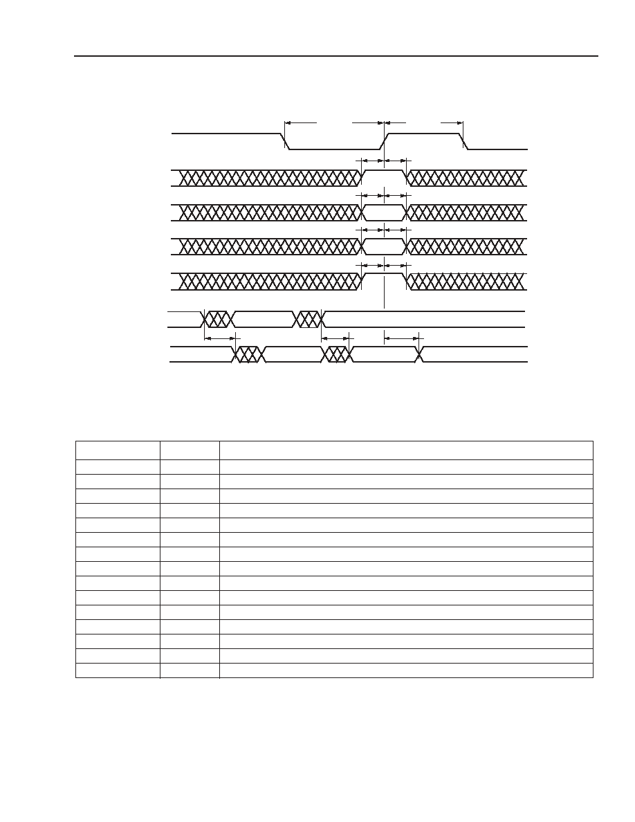
Lattice Semiconductor
29
Data Sheet
March, 2003
ORCA
Series 4 FPGAs
Embedded Block RAM
(continued)
0308(F)
Figure 21. EBR Read and Write Cycles with Write Through and Nonregistered Read Port
Table 9. FIFO Signals
Port Signals
I/O
Function
AR0[5:0]
I
Programs FIFO flags. Used for partially empty flag size.
AR1[9:0]
I
Programs FIFO flags. Used for partially full flag size.
FF
O
Full Flag.
PFF
O
Partially Full Flag.
PEF
O
Partially Empty Flag.
EF
O
Empty Flag.
D0[17:0]
I
Data inputs for all configurations.
D1[17:0]
I
Data inputs for 256x36 configurations only.
CKW[0:1]
I
Positive-edge write port clock. Port 1 only used for 256x36 configurations.
CKR[0:1]
I
Positive-edge read port clock. Port 1 only used for 256x36 configurations.
CSW[1:0]
I
Active-high write enable. Port 1 only used for 256x36 configurations.
CSR[1:0]
I
Active-high read enable. Port 1 only used for 256x36 configurations.
RESET
I
Active-low Resets FIFO pointers.
Q0[17:0]
O
Data outputs for all configurations.
Q1[17:0]
O
Data outputs for 256x36 configurations.
CKWPH
CKWPL
CSWSU
CSWH
AWH
DSU
DH
BWSU
BWH
AWSU
CKWQ
AQ
AQH
a
b
c
d
b
c
a
d
c
CKW
CSW
AW
D
BW
AR
Q

30
Lattice Semiconductor
Data Sheet
March, 2003
ORCA
Series 4 FPGAs
Embedded Block RAM
(continued)
Table 10. Constant Multiplier Signals
Table 11. 8x8 Multiplier Signals
Table 12. CAM Signals
Port Signals
I/O
Function
AR0[15:0]
I
Data input�operand.
AW(1:0)[8:0]
I
Address bits.
D(1:0)[17:0]
I
Data inputs to load memory or change coefficient.
CKW[0:1]
I
Positive-edge write port clock.
CKR[0:1]
I
Positive-edge read port clock. Used for synchronous multiply mode.
CSW[1:0]
I
Active-high write enable.
CSR[1:0]
I
Active-high read enable.
Q[23:0]
O
Data outputs�product result.
Port Signals
I/O
Function
AR0[7:0]
I
Data input-Multiplicand.
AR1[7:0]
I
Data input-Multiplier.
CKR[0:1]
I
Positive-edge read port clock. Used for synchronous multiply mode.
CSR[1:0]
I
Active-high read enable.
Q[15:0]
O
Data outputs-product.
Port Signals
I/O
Function
AR(1:0)[7:0]
I
Data Match.
AW(1:0)[8:0]
I
Data Write.
D(1:0)[17]
I
Clear data active high.
D(1:0)[16]
I
Single match active high.
D(1:0)[3:0]
I
CAM address for data write.
CSW[1:0]
I
Active-high write enable. Enable for CAM data write.
CSR[1:0]
I
Active-high read enable. Enable for CAM data match.
Q(1:0)15:0]
O
Decoded Data outputs. "1" corresponds to a data match at that address location.

Lattice Semiconductor
31
Data Sheet
March, 2003
ORCA
Series 4 FPGAs
Routing Resources
The abundant routing resources of the Series 4 archi-
tecture are organized to route signals individually or as
buses with related control signals. Both local and glo-
bal signals utilize high-speed buffered and nonbuffered
routes. One PLC segmented (x1), six PLC segmented
(x6), and bused half chip (xHL) routes are patterned
together to provide high connectivity with fast software
routing times and high-speed system performance.
x1 routes cross width of one PLC and provide local
connectivity to PFU and SLIC inputs and outputs. x6
lines cross width of 6 PLCs and are unidirectional and
buffered with taps in the middle and on the end. Seg-
ments allow connectivity to PFU/SLIC outputs (driven
at one end-point), other x6 lines (at end-points), and
x1 lines for access to PFU/SLIC inputs. xH lines run
vertically and horizontally the distance of half the
device and are useful for driving medium/long distance
3-state routing.
The improved routing resources offer great flexibility in
moving signals to and from the logic core. This flexibil-
ity translates into an improved capability to route
designs at the required speeds even when the I/O sig-
nals have been locked to specific pins. The buffered
routing capability also allows a very large fanout to be
driven from each logic output, thus greatly reducing the
amount of logic replication required by synthetic tools.
Generally, the ispLEVER Development System is used
to automatically route interconnections. Interactive
routing with the ispLEVER design editor (EPIC) is also
available for design optimization.
The routing resources consist of switching circuitry and
metal interconnect segments. Generally, the metal
lines which carry the signals are designated as routing
segments. The switching circuitry connects the routing
segments, providing one or more of three basic func-
tions: signal switching, amplification, and isolation. A
net running from a PFU, EBR, or PIO output (source) to
a PLC, EBR, or PIO input (destination) consists of one
or more routing segments, connected by switching cir-
cuitry called configurable interconnect points (CIPs).
Clock Distribution Network
Clock distribution is made up of three types of clock
networks: primary, secondary, and edge clocks. these
are described below and more information is available
in the Series 4 Clocking Strategies application note.
Global Primary Clock Nets
The Series 4 FPGAs provide eight fully distributed glo-
bal primary clock net routing resources. The scheme
dedicates four of the eight resources to provide fast pri-
mary nets and four are available for general primary
nets. The fast primary nets are targeted toward low-
skew and small injection times while the general pri-
mary nets are also targeted toward low-skew but have
more source connection flexibility. Fast access to the
global primary nets can be sourced from two pairs of
pads located in the center of each side of the device,
from the programmable PLLs and dedicated network
PLLs located in the corners, or from general routing at
the center of the device or at the middle of any side of
the device. The I/O pads are semi-dedicated in pairs for
use of differential I/O clocking or single-ended I/O clock
sources. However if these pads are not needed to
source the clock network they can be utilized for gen-
eral I/O. The clock routing scheme is patterned using
vertical and horizontal routes which provide connectiv-
ity to all PLC columns.
Secondary Clock and Control Nets
Secondary clock control and routing provides flexible
clocking and control signalling for local regions. Since
secondary nets usually have high fanouts and require
low skew, the Series 4 devices utilize a spine and
branch that uses x6 segments with high-speed connec-
tions provided from the spines to the branches. The
branches then have high-speed connections to PLC,
PIO, and EBR clock and control signals. This strategy
provides a flexible connectivity and routes can be
sourced from any I/O pin, all PLLs, or from PLC or EBR
logic.
Secondary Edge Clock Nets and Fast Edge
Clock Nets
Six secondary edge clock nets per side are distributed
around the edges of the device and are available for
every PIO. All PIOs and PLLs can drive the secondary
edge clocks and are used in conjunction with the sec-
ondary spines discussed above to drive the same edge
clock signal into the internal logic array. The edge sec-
ondary clocks provide fast injection to the PLC array
and I/O registers. One of the six secondary edge
clocks provided per side of the device is a special fast
edge clock net that only clocks input registers for fur-
ther reduced setup/hold times.This timing path can only
be driven from one of the four PIO input pins in each
PIC.

32
32
Lattice Semiconductor
Data Sheet
March, 2003
ORCA
Series 4 FPGAs
Routing Resources
(continued)
Cycle Stealing
A new feature in Series 4 FPGAs is the ability to steal
time from one register-to-register path and use that
time in either the previous path before the first register
or in a later path after the last register. This is done
through selectable clock delays for every PLC register,
EBR register, and PIO register. There are four pro-
grammable delay settings, including the default zero
added delay value. This allows performance increases
on typical critical paths from 15% to 40%. ispLEVER
includes software to automatically take advantage of
this capability to increase overall system speed. This is
done after place and route is completed and uses tim-
ing driven algorithms based on the customer's prefer-
ence file. A hold time check is also performed to verify
no minimum hold time issues are introduced. More
information on this clocking feature, including how it
can be used to improve device setup times, hold times,
clock-to-out delays and can reduce ground bounce
caused by switching outputs can be found in the Cycle
Stealing application note.
Programmable Input/Output Cells (PIC)
Programmable I/O
The Series 4 programmable I/O addresses the demand
for the flexibility to select I/O that meets system inter-
face requirements. I/Os can be programmed in the
same manner as in previous ORCA devices with the
addition of new features which allow the user the flexi-
bility to select new I/O types that support high-speed
interfaces.
Each PIC contains up to four programmable I/O (PIO)
pads and are interfaced through a common interface
block (CIB) to the FPGA array. The PIC is split into two
pairs of I/O pads with each pair having independent
clocks, clock enables, local set/reset, and global
set/reset enable/disable.
On the input side, each PIO contains a programmable
latch/FF which enables very fast latching of data from
any pad. The combination provides for very low setup
requirements and zero hold times for signals coming
on-chip. It may also be used to demultiplex an input sig-
nal, such as a multiplexed address/data signal, and
register the signals without explicitly building a demulti-
plexer with a PFU.
On the output side of each PIO, an output from the PLC
array can be routed to each output FF, and logic can be
associated with each I/O pad. The output logic associ-
ated with each pad allows for multiplexing of output sig-
nals and other functions of two output signals.
The output FF, in combination with output signal multi-
plexing, is particularly useful for registering address
signals to be multiplexed with data, allowing a full clock
cycle for the data to propagate to the output. The out-
put buffer signal can be inverted, and the 3-state con-
trol can be made active-high, active-low, or always
enabled. In addition, this 3-state signal can be regis-
tered or nonregistered.
The Series 4 I/O logic has been enhanced to include
modes for high-speed uplink and downlink capabilities.
These modes are supported through shift register logic
which divides down incoming data or multiplies up out-
going data. This new logic block also supports high-
speed DDR mode requirements where data is clocked
into and out of the I/O buffers on both edges of the
clock.
The new programmable I/O cell allows designers to
select I/Os which meet many new communication stan-
dards permitting the device to hook up directly without
any external interface translation. They support tradi-
tional FPGA standards as well as high-speed single-
ended and differential pair signaling (as shown in
Table 13). Based on a programmable, bank-oriented
I/O ring architecture, designs can be implemented
using 3.3 V, 2.5 V, 1.8 V, and 1.5 V I/O levels.
The I/O on the OR4Exx Series devices allows compli-
ance with PCI local bus (Rev. 2.2) 3.3 V signaling envi-
ronments. The signaling environment used for each
input buffer can be selected on a per-pin basis. The
selection provides the appropriate I/O clamping diodes
for PCI compliance.
More information on the Series 4 programmable I/O
structure is available in the various application notes.

Lattice Semiconductor
33
Data Sheet
March, 2003
ORCA
Series 4 FPGAs
Programmable Input/Output Cells
(continued)
Table 13. Series 4 Programmable I/O Standards
Note: interfaces to DDR and ZBT memories are supported through the interface standards shown above.
The PIOs are located along the perimeter of the device. The PIO name is represented by a two-letter designation to
indicate the side of the device on which it is located followed by a number to indicate the row or column in which it is
located. The first letter, P, designates that the cell is a PIO and not a PLC. The second letter indicates the side of the
array where the PIO is located. The four sides are left (L), right (R), top (T), and bottom (B). A number follows to
indicate the PIC row or column. The individual I/O pad is indicated by a single letter (either A, B, C, or D) placed at
the end of the PIO name. As an example, PL10A indicates a pad located on the left side of the array in the tenth
row.
Each PIC interfaces to four bond pads through four PIOs and contains the necessary routing resources to provide
an interface between I/O pads and the CIBs. Each PIC contains input buffers, output buffers, routing resources,
latches/FFs, and logic and can be configured as an input, output, or bidirectional I/O. Any PIO is capable of sup-
porting the I/O standards listed in Table 13.
The CIBs that connect to the PICs have significant local routing resources, similar to routing in the PLCs. This new
routing increases the ability to fix user pinouts prior to placement and routing of a design and still maintain routabil-
ity. The flexibility provided by the routing also provides for increased signal speed due to a greater variety of optimal
signal paths.
Included in the routing interface is a fast path from the input pins to the PFU logic. This feature allows for input sig-
nals to be very quickly processed by the SLIC decoder function and used on-chip or sent back off of the FPGA.
A diagram of a single PIO is shown in Figure 22, and Table 14 provides an overview of the programmable functions
in an I/O cell.
Standard
V
DD
IO (V)
V
REF
(V)
Interface Usage
LVTTL
3.3
NA
General purpose.
LVCMOS2
2.5
NA
LVCMOS18
1.8 NA
PCI
3.3
NA
PCI.
LVDS
2.5
NA
Point to point and multi-drop backplanes, high noise immunity.
Bused-LVDS
2.5
NA
Network backplanes, high noise immunity, bus architecture
backplanes.
LVPECL
3.3
NA
Network backplanes, differential 100 MHz+ clocking, optical
transceiver, high-speed networking.
PECL
3.3
2.0
Backplanes.
GTL
3.3
0.8
Backplane or processor interface.
GTL+
3.3
1.0
HSTL-class I
1.5
0.75
High-speed SRAM and networking interfaces.
HTSL-class III and IV
1.5
0.9
STTL3-class I and II
3.3
1.5
Synchronous DRAM interface.
SSTL2-class I and II
2.5
1.25
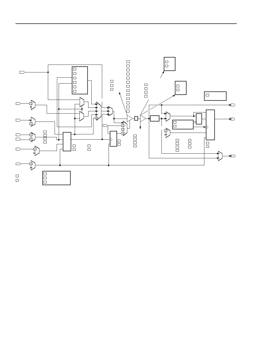
34
Lattice Semiconductor
Data Sheet
March, 2003
ORCA
Series 4 FPGAs
Programmable Input/Output Cells
(continued)
5-9732(F)
Figure 22. Series 4 PIO Image from ispLEVER Design Software
OUTSH
OUTDDMUX
OUTDD
OUTFFMUX
OUTFF
CLK4MUX
EC
SC
CE
LSRMUX
LSR
GSR
ENABLED
DISABLED
SRMODE
CE_OVER_LSR
LSR_OVER_CE
ASYNC
CEMUX0
OUTDD
CLK
OUTSH
CLK
OUTDD
OUTREG
OUTREG
DO
CK
SP
LSR
AND
NAND
OR
NOR
XOR
XNOR
PLOGIC
PMUX
OUTSHMUX
BUFMODE
SLEW
FAST
LEVELMODE
PCI
SSTL2
SSTL3
HSTL1
HSTL3
GTL
GTLPLUS
PECL
LVPECL
LVDS
P2MUX
OUTDD
TSMUX
USRTS
TSREG
DO
CK
LSR
RESET
SET
PULLMODE
UP
DOWN
NONE
INMUX
CEMUXI
NORMAL
INVERTED
LATCHFF
D0
D1
CK
SP
LSR
D0
CK
LATCHFF
LATCH
FF
INDDMUX
INDD
INCK
INFF
RESET
SET
RESET
SET
1
0
0
0
0
1
EC
SC
DELAY
IOPAD
OUTMUX
CELL
CE
1
LVCMOS2
LVCMOS18
DEL0
DEL1
DEL2
DEL3
DEL0
DEL1
DEL2
DEL3
MILLIAMPS
SIX
TWELVE
TWENTYFOUR
RESISTOR
OFF
ON
KEEPERMODE
OFF
ON
LATCH
FF
OUTPUT SIDE
INPUT SIDE
LVTTL
NA
NA
NA
LVDS
FAST INPUT

Lattice Semiconductor
35
Data Sheet
March, 2003
ORCA
Series 4 FPGAs
Programmable Input/Output Cells
(continued)
Inputs
There are many major options on the PIO inputs that
can be selected in the ispLEVER tools listed in Table
14. Inputs may have a pull-up or pull-down resistor
selected on an input for signal stabilization and power
management. Input signals in a PIO are passed to CIB
routing and/or a fast route into the clock routing sys-
tem. A fast input from one PIO per PIC is also available
to drive the edge clock network for fast I/O timing to
other nearby PIOs.
There is also a programmable delay available on the
input. When enabled, this delay affects the INFF and
INDD signals of each PIO, but not the clock input. The
delay allows any signal to have a guaranteed zero hold
time when input.
Inputs should have transition times of less than 100 ns
and should not be left floating. For full swing inputs, the
timing characterization is done for rise/fall times of
1 V/ns. If any pin is not used, it is 3-stated with an
internal pull-up resistor enabled automatically after
configuration. Floating inputs increase power con-
sumption, produce oscillations, and increase system
noise. The inputs in LVTTL, LVCMOS2, and
LVCMOS18 modes have a typical hysteresis of approx-
imately 250 mV to reduce sensitivity to input noise. The
PIC contains input circuitry which provides protection
against latch-up and electrostatic discharge.
The other features of the PIO inputs relate to the latch/
FF structure in the input path. In latch mode, the input
signal is fed to a latch that is clocked by either the pri-
mary, secondary, or edge clock signal. The clock may
be inverted or noninverted. There is also a local set/
reset signal to the latch. The senses of these signals
are also programmable as well as the capability to
enable or disable the global set/reset signal and select
the set/reset priority. The same control signals may
also be used to control the input latch/FF when it is
configured as a FF instead of a latch, with the addition
of another control signal used as a clock enable. The
PIOs are paired together and have independent CE,
Set/reset, and GSRN control signals per PIO pair.
There are two options for zero-hold input capture in the
PIO. If input delay mode is selected to delay the signal
from the input pin, data can be either registered or
latched with guaranteed zero-hold time in the PIO
using a global primary system clock. The fast zero-hold
mode of the PIO input takes advantage of a latch/FF
combination to latch the data quickly for zero-hold
using a fast edge clock before passing the data to the
FF which is clocked by a global primary system clock.
The combination of input register capability with non-
registered inputs provides for input signal demultiplex-
ing without any additional resources. The PIO input
signal is sent to both the input register and directly to
the unregistered input (INDD). The signal is latched
and output to routing at INFF. These signals may then
be registered or otherwise processed in the PLCs.
Every PIO input can also perform input double data
rate (DDR) functions with no PLC resources required.
This type of scheme is necessary for DDR applications
which require data to be clocked in from the I/O on both
edges of the clock. In this scheme the input of INFF
and INSH are captured on the positive and negative
edges of the clock.
Table 14. PIO Options
Input
Option
Input Speed
Fast, Delayed, Normal
Float Value
Pull-up, Pull-down, None
Register Mode
Latch, FF, Fast Zero Hold FF,
None (direct input)
Clock Sense
Inverted, Noninverted
Keeper Mode
on, off
LVDS Resistor
on, off
Output
Option
Output Speed
Fast, Slew
Output Drive
Current
12 mA/6 mA, 6 mA/3 mA, or
24 mA/12 mA
Output Function
Normal, Fast Open Drain
Output Sense
Active-high, Active-low
3-State Sense
Active-high, Active-low
Clock Sense
Inverted, Noninverted
Logic Options
See Table 15
I/O Controls
Option
Clock Enable
Active-high, Active-low,
Always Enabled
Set/Reset Level
Active-high, Active-low,
No Local Reset
Set/Reset Type
Synchronous, Asynchronous
Set/Reset Priority
CE over LSR, LSR over CE
GSR Control
Enable GSR, Disable GSR

36
36
Lattice Semiconductor
Data Sheet
March, 2003
ORCA
Series 4 FPGAs
Programmable Input/Output Cells
(continued)
Outputs
The PIO's output drivers have programmable drive
capability and slew rates. Two propagation delays (fast,
slewlim) are available on output drivers. There are
three combinations of programmable drive currents
(24 mA sink/12 mA source, 12 mA sink/6 mA source,
and 6 mA sink/3 mA source). At powerup, the output
drivers are in slewlim mode with 12mA sink/6 mA
source. If an output is not to be driven in the selected
configuration mode, it is 3-stated with a pullup resistor.
The output buffer signal can be inverted, and the
3-state control signal can be made active-high, active-
low, or always enabled. In addition, this 3-state signal
can be registered or nonregistered. Additionally, there
is a fast, open-drain output option that directly connects
the output signal to the 3-state control, allowing the out-
put buffer to either drive to a logic 0 or 3-state, but
never to drive to a logic 1.
Every PIO output can perform output data multiplexing
with no PLC resources required. This type of scheme is
necessary for DDR applications which require data
clocking out of the I/O on both edges of the clock. In
this scheme the OUTFF and OUTSH are registered
and sent out on both the positive and negative edges of
the clock using an output multiplexor. This multiplexor
is controlled by either the edge clock or system clock.
This multiplexor can also be configured to select
between one registered output from OUTFF and one
nonregistered output from OUTDD.
The PIC logic block can also generate logic functions
based on the signals on the OUTDD and CLK ports of
the PIO. The functions are AND, NAND, OR, NOR,
XOR, and XNOR. Table 15 is provided as a summary
of the PIO logic options.
Table 15.
PIO Logic Options
PIO Register Control Signals
The PIO latches/FFs have various clock, clock enable
(CE), local set/reset (LSR), and GSRN controls. Table
16 provides a summary of these control signals and
their effect on the PIO latches/FFs. Note that all control
signals are optionally invertible.
Table 16. PIO Register Control Signals
Option
Description
AND
Output logical AND of signals on OUTDD
and clock.
NAND
Output logical NAND of signals on OUTDD
and clock.
OR
Output logical OR of signals on OUTDD
and clock.
NOR
Output logical NOR of signals on OUTDD
and clock.
XOR
Output logical XOR of signals on OUTDD
and clock.
XNOR Output logical XNOR of signals on OUTDD
and clock.
Control
Signal
Effect/Functionality
Edge Clock
(ECLK)
Clocks input fast-capture latch; option-
ally clocks output FF, or
3-state FF, or PIO shift registers.
System
Clock
(SCLK)
Clocks input latch/FF; optionally clocks
output FF, or 3-state FF, or PIO shift
registers.
Clock
Enable (CE)
Optionally enables/disables input FF
(not available for input latch mode);
optionally enables/disables output FF;
separate CE inversion capability for
input and output.
Local Set/
Reset (LSR)
Option to disable; affects input latch/FF,
output FF, and 3-state FF if enabled.
Global Set/
Reset
(GSRN)
Option to enable or disable per PIO
after initial configuration.
Set/Reset
Mode
The input latch/FF, output FF, and 3-
state FF are individually set or reset by
both the LSR and GSRN inputs.

Lattice Semiconductor
37
Data Sheet
March, 2003
ORCA
Series 4 FPGAs
Programmable Input/Output Cells
(continued)
I/O Banks and Groups
Flexible I/O features allow the user to select the type of
I/O needed to meet different high-speed interface
requirements and these I/Os require different input ref-
erences or supply voltages. The perimeter of the device
is divided into eight banks of PIO buffers, as shown in
Figure 23, and for each bank there is a separate V
DD
IO
that supplies the correct input and output voltage for a
particular standard. The user must supply the appropri-
ate power supply to the V
DD
IO pin. Within a bank, sev-
eral I/O standards may be mixed as long as they use a
common V
DD
IO. The shaded section of the I/O banks in
Figure 23 (banks 2, 3, and 4) are removed for FPSCs,
to allow the embedded block to be placed on the side
of the FPGA array. Bank 1 and bank 5 are also
extended to the corners in FPSCs to incorporate more
FPGA I/Os.
Some interface standards require a specified threshold
voltage known as V
REF.
To accommodate various V
REF
requirements, each bank is further divided into groups.
In these modes, where a particular V
REF
is required,
the device is automatically programmed to dedicate a
V
REF
pin for each group of PIOs within a bank. The
appropriate V
REF
voltage must be supplied by the user
and connected to the V
REF
pin for each group. The
V
REF
is dedicated exclusively to the group and cannot
be intermixed within the group with other signaling
requiring other V
REF
voltages. However, pins not
requiring V
REF
can be mixed in the same group. When
used to supply a reference voltage the V
REF
pad is no
longer available to the user for general use. The V
REF
inputs should be well isolated to keep the reference
voltage at a consistent level.
Table 17
. Compatible Mixed I/O Standards
0205(F).
Figure 23. ORCA High-Speed I/O Banks
Differential I/O (LVDS and LVPECL)
Series 4 devices support differential input, output, and
input/output capabilities through pairs of PIOs. The two
standards supported are LVDS and LVPECL.
The LVDS differential pair I/O standard allows for high-
speed, low-voltage swing and low-power interfaces
defined by industry standards: ANSI/TIA/EIA-644 and
IEEE 1596.3 SSI-LVDS
. The general purpose standard
is supplied without the need for an input reference sup-
ply and uses a low switching voltage which translates
to low ac power dissipation.
The ORCA LVDS I/O provides an integrated 100
ter-
mination resistor used to provide a differential voltage
across the inputs of the receiver. The on-chip integra-
tion provides termination of the LVDS receiver without
the need of discrete external board resistors. The user
has the programmable option to enable termination per
receiver pair for point-to-point applications or in multi-
point interfaces limit the use of termination to bussed
pairs. If the user chooses to terminate any differential
receiver, a single LVDS_R pin is dedicated to connect a
single 100
(� 1%) resistor to V
SS
which then enables
an internal resistor matching circuit to provide a bal-
ance 100
(� 10%) termination across all process,
voltage, and temperature. Experiments have also
shown that enabling this 100
matching resistor for
LVDS outputs also improves performance.
V
DD
IO
Bank
Voltage
Compatible Standards
3.3 V
LVTTL, SSTL3-I, SSTL3-II, GTL+,
GTL, LVPECL, PECL
2.5 V
LVCMOS2, SSTL2-I, SSTL2-II, LVDS
1.8 V
LVCMOS18
1.5 V
HSTL I, HSTL III, HSTL IV
PLC ARRAY
(TC)
(TL)
(BC)
(BL)
(CL)
BANK 0
BANK 1
BANK 5
BANK 6
BANK 7
(TR)
(BR)
(CR)
BANK 2
BANK 3
BANK 4

38
38
Lattice Semiconductor
Data Sheet
March, 2003
ORCA
Series 4 FPGAs
Programmable Input/Output Cells
(continued)
High-Speed Memory Interfaces
PIO features allow high-speed interfaces to external
SRAM and/or DRAM devices. Series 4 I/O meet
200 MHz ZBT requirements when switching between
write and read cycles. ZBT allows 100% use of bus
cycles during back-to-back read/write and write/read
cycles. However this maximum utilization of the bus
increases probability of bus contention when the inter-
faced devices attempt to drive the bus to opposite logic
values. The LVTTL I/O interfaces directly with commer-
cial ZBT SRAMs signalling and allows the versatility to
program the FPGA drive strengths from 6 mA to
24 mA.
DDR allows data to be read on both the rising and the
falling edge of the clock which delivers twice the band-
width. DDR doubles the memory speed from SDRAMs
or SRAMs without the need to increase clock fre-
quency. The flexibility of the PIO allows at least
156 MHz/312 Mbits per second performance using the
SSTL I/O or HSTL I/O features of the Series 4 devices.
High-Speed Networking Interfaces
Series 4 devices support many I/O standards used in
networking. Two examples of this are the XGMII stan-
dard for 10 GbE (HSTL or SSTL I/Os) and the SPI-4
standard for various 10 Gbits/s network interfaces
(LVDS I/Os). Both operate as a point-to-point link
between devices that are forward clocked and transmit
data on both clock edges (DDR). The XGMII interface
is 36-bits wide per data flow direction and the SPI-4
interface is a 16-bit interface. The XGMII specification
is 156 MHz/312 Mbits/s and the SPI-4 specification that
can be met is 325 MHz/650 Mbits/s. More information
about using ORCA for these applications can be found
in the associated application note.
Bus Hold
Each PIO can be programmed with a KEEPERMODE
feature. This element is user programmed for bus hold
requirements. This mode retains the last known state of
a bus when the bus goes into 3-state. It prevents float-
ing busses and saves system power.
PIO Downlink/Uplink (Shift Registers)
Each group of four PIOs in a PIC have access to an
input/output shift register as shown in Figure 24. This
feature allows high-speed input data to be divided
down by 1/2 or 1/4 and output data can be multiplied by
2x or 4x its internal speed. Both the input and output
shift registers can be programmed to operate at the
same time and are controlled by the same clock and
control signals.
For input shift mode, the data from INDD from the PIO
is connected to the input shift register. The input data is
divided down and is driven to the routing through the
INSH nodes. For output shift mode, the data from the
OUTSH nodes are driven from the internal routing and
connects to the output shift register. This output data is
multiplied up and driven to the OUTDD signal on the
PIOs.
In 2x output mode or input mode, two of the four I/Os in
a PIC can use the shift registers. While in 4x mode,
only one I/O can use the shift registers. This also
means that all differential I/Os on a Series 4 device can
use 2x shift register mode, but 4x mode is only avail-
able for half of the differential I/Os.
In 4x input mode, all the INSH nodes are used, while 2x
mode uses INSH4 and INSH3 for one shift register and
INSH2 and INSH1 for the second shift register. Simi-
larly, the output shift register in 4x mode uses all the
OUTSH signals. OUTSH2 and OUTSH1 are used for
2x output mode for one shift register and OUTSH4 and
OUTSH3 are used for the other output shift register.
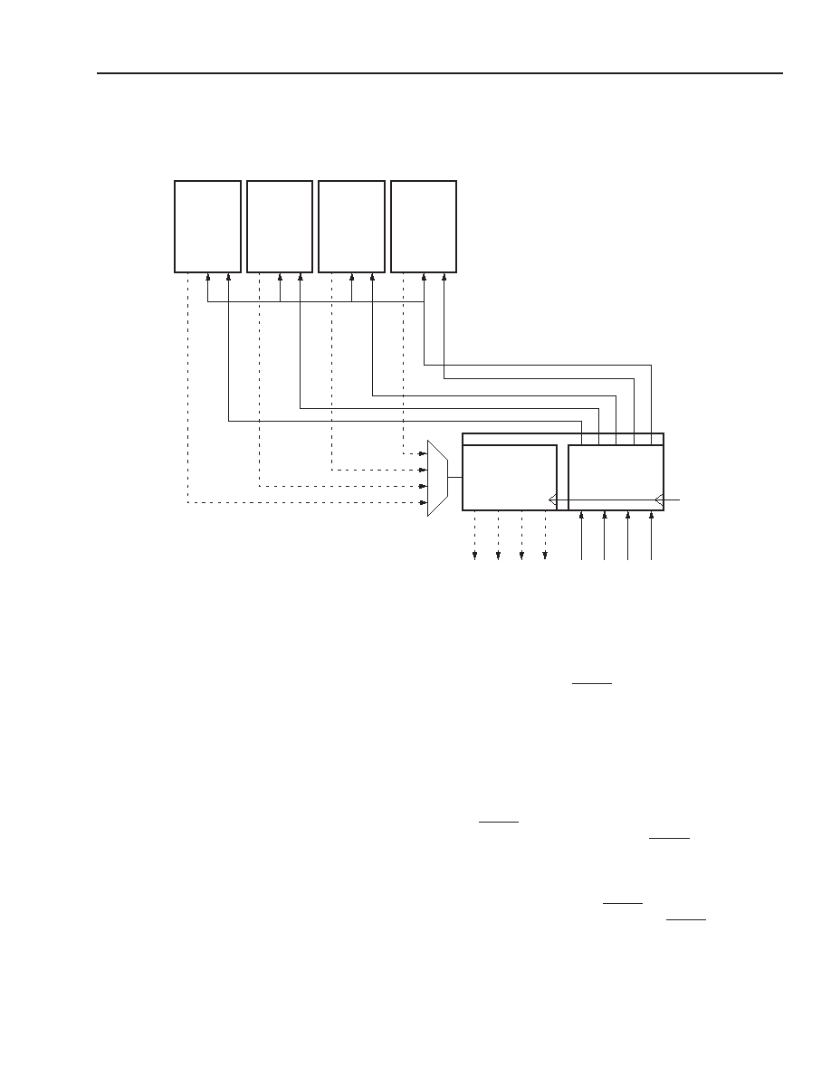
Data Sheet
March, 2003
Lattice Semiconductor
39
ORCA
Series 4 FPGAs
Programmable Input/Output Cells
(continued)
0204(F).
Figure 24. PIO Shift Register
INDD
OUTSH
OUTDD
PIO
INDD
OUTSH
OUTDD
PIO
INDD
OUTSH
OUTDD
PIO
INDD
OUTSH
OUTDD
PIO
SHIFT REGISTER
OUT FROM FPGA
SHIFT REGISTER
INTO FPGA
CLK
OUTSH1
OUTSH2
OUTSH3
OUTSH4
INSH1
INTSH2
INSH3
INSH4
Special Function Blocks
Special function blocks in the Series 4 provide extra
capabilities beyond general FPGA operation. These
blocks reside in the corners and MIDs (middle inter-
quad areas) of the FPGA array.
Internal Oscillator
The internal oscillator resides in the upper left corner of
the FPGA array. It has output clock frequencies of
1.25 MHz and 10 MHz. The internal oscillator is the
source of the internal CCLK used for configuration. It
may also be used after configuration as a general-
purpose clock signal.
Global Set/Reset (GSRN)
The GSRN logic resides in the upper-left corner of the
FPGA. GSRN is an invertible, default, active-low signal
that is used to reset all of the user-accessible latches/
FFs on the device. GSRN is automatically asserted at
powerup and during configuration of the device.
The timing of the release of GSRN at the end of config-
uration can be programmed in the start-up logic
described below. Following configuration, GSRN may
be connected to the
RESET
pin via dedicated routing, or
it may be connected to any signal via normal routing.
GSRN can also be controlled via a system bus register
command. Within each PFU and PIO, individual FFs
and latches can be programmed to either be set or
reset when GSRN is asserted. Series 4 allows individ-
ual PFUs and PIOs to turn off the GSRN signal to its
latches/FFs after configuration.
The
RESET
input pad has a special relationship to
GSRN. During configuration, the
RESET
input pad
always initiates a configuration abort, as described in
the FPGA States of Operation section. After configura-
tion, the GSRN can either be disabled (the default),
directly connected to the
RESET
input pad, or sourced
by a lower-right corner signal. If the
RESET
input pad is
not used as a global reset after configuration, this pad
can be used as a normal input pad.
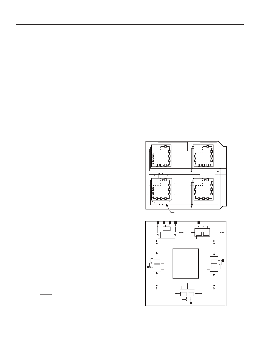
40
40
Lattice Semiconductor
Data Sheet
March, 2003
ORCA
Series 4 FPGAs
Special Function Blocks
(continued)
Start-Up Logic
The start-up logic block can be configured to coordi-
nate the relative timing of the release of GSRN, the
activation of all user I/Os, and the assertion of the
DONE signal at the end of configuration. If a start-up
clock is used to time these events, the start-up clock
can come from CCLK, or it can be routed into the start-
up block using upper-left corner routing resources.
Temperature Sensing
The built-in temperature-sensing diodes allow junction
temperature to be measured during device operation. A
physical pin (PTEMP) is dedicated for monitoring
device junction temperature. PTEMP works by forcing
a 10 �A current in the forward direction, and then mea-
suring the resulting voltage. The voltage decreases
with increasing temperature at approximately
�1.69 mV/�C. A typical device with a 85�C device tem-
perature will measure approximately 630 mV.
Boundary-Scan
The IEEE standards 1149.1 and 1149.2 (IEEE Stan-
dard test access port and boundary-scan architecture)
are implemented in the ORCA series of FPGAs. It
allows users to efficiently test the interconnection
between integrated circuits on a PCB as well as test
the integrated circuit itself. The IEEE 1149 standard is
a well-defined protocol that ensures interoperability
among boundary-scan (BSCAN) equipped devices
from different vendors.
Series 4 FPGAs are also compliant to IEEE standard
1532/D1. This standard for boundary-scan based in-
system configuration of programmable devices pro-
vides a standardized programming access and meth-
odology for FPGAs. A device, or set of devices,
implementing this standard may be programmed, read
back, erased verified, singly or concurrently, with a
standard set of resources.
The IEEE 1149 standards define a test access port
(TAP) that consists of a four-pin interface with an
optional reset pin for boundary-scan testing of inte-
grated circuits in a system. The ORCA Series FPGA
provides four interface pins: test data in (TDI), test
mode select (TMS), test clock (TCK), and test data out
(TDO). The
PRGM
pin used to reconfigure the device
also resets the boundary-scan logic.
The user test host serially loads test commands and
test data into the FPGA through these pins to drive out-
puts and examine inputs. In the configuration shown in
Figure 26, where boundary-scan is used to test ICs,
test data is transmitted serially into TDI of the first
BSCAN device (U1), through TDO/TDI connections
between BSCAN devices (U2 and U3), and out TDO of
the last BSCAN device (U4). In this configuration, the
TMS and TCK signals are routed to all boundary-scan
ICs in parallel so that all boundary-scan components
operate in the same state. In other configurations, mul-
tiple scan paths are used instead of a single ring. When
multiple scan paths are used, each ring is indepen-
dently controlled by its own TMS and TCK signals.
Figure 26 provides a system interface for components
used in the boundary-scan testing of PCBs. The three
major components shown are the test host, boundary-
scan support circuit, and the devices under test
(DUTs). The DUTs shown here are ORCA Series
FPGAs with dedicated boundary-scan circuitry. The
test host is normally one of the following: automatic test
equipment (ATE), a workstation, a PC, or a micropro-
cessor.
5-5972(F)
Key:BSC = boundary-scan cell, BDC = bidirectional data cell, and
DCC = data control cell.
Figure 25. Printed-Circuit Board with
Boundary-Scan Circuitry
INSTRUCTION
TDO
REGISTER
BYPASS
REGISTER
TCK TMS TDI
SCAN
OUT
SCAN
IN
SCAN
OUT
SCAN
IN
SCAN
IN
SCAN
OUT
BSC
BDC
DCC
SCAN
OUT
SCAN
IN
TAPC
p_in
p_in
p_out
p_in
p_ts
p_out
p_ts
p_in
p_out
p_ts
p_out
p_ts
PL[ij]
PT[ij]
PR[ij]
PB[ij]
BDC
DCC
PLC
ARRAY
BDC
DCC
BDC
DCC
BSC
BSC
BSC
SEE ENLARGED VEIW BELOW
TMS TDI
TCK
TDO
TMS TDI
TCK
TDO
TMS TDI
TCK
TDO
TMS TDI
TCK
TDO
U1
U2
U3
U4
TDI
TCK
TDO
TMS
net a
net b
net c
S
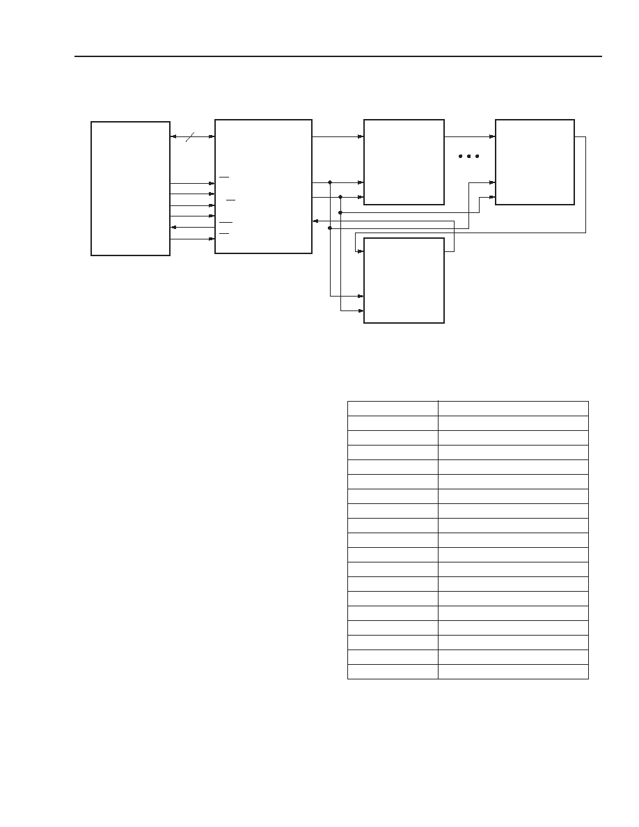
Data Sheet
March, 2003
Lattice Semiconductor
41
ORCA
Series 4 FPGAs
Special Function Blocks
(continued)
5-6765(F)
Figure 26. Boundary-Scan Interface
D[7:0]
INTR
MICRO-
PROCESSOR
D[7:0]
CE
RA
R/W
DAV
INT
SP
TMS0
TCK
TDI
TDO
TDI
TMS
TCK
TDO
ORCA
SERIES
FPGA
TDI
ORCA
SERIES
FPGA
TMS
TCK
TDO
TDI
TMS
TCK
TDO
ORCA
SERIES
FPGA
BOUNDARY-
SCAN
MASTER
(BSM)
(DUT)
(DUT)
(DUT)
The boundary-scan support circuit shown in Figure 26
is the 497AA boundary-scan master (BSM). The BSM
off-loads tasks from the test host to increase test
throughput. To interface between the test host and the
DUTs, the BSM has a general MPI and provides paral-
lel-to-serial/serial-to-parallel conversion, as well as
three 8K data buffers. The BSM also increases test
throughput with a dedicated automatic test-pattern
generator and with compression of the test response
with a signature analysis register. The PC-based
boundary-scan test card/software allows a user to
quickly prototype a boundary-scan test setup.
Boundary-Scan Instructions
The Series 4 boundary-scan circuitry supports a total
of 18 instructions. This includes ten IEEE 1149.1,
1149.2, and 1532/D1 instructions, one optional IEEE
1149.3 instruction, two IEEE 1532/D1 optional instruc-
tions, and five ORCA-defined instructions. There are
also 16 other scan chain instructions that are used only
during factory device testing and will not be discussed
in this data sheet. A 6-bit wide instruction register sup-
ports all the instructions listed in Table 18.
The BYPASS instruction passes data intentionally from
TDI to TDO after being clocked by TCK.
Table 18. Boundary-Scan Instructions
Code
Instruction
000000
EXTEST
000001
SAMPLE
000011
PRELOAD
000100
RUNBIST
000101
IDCODE
000110
USERCODE
001000
ISC_ENABLE
001001
ISC_PROGRAM
001010
ISC_NOOP
001011
ISC_DISABLE
001101
ISC_PROGRAM_USERCODE
001110
ISC_READ
010001
PLC_SCAN_RING1
010010
PLC_SCAN_RING2
010011
PLC_SCAN_RING3
010100
RAM_WRITE
010101
RAM_READ
111111
BYPASS

42
42
Lattice Semiconductor
Data Sheet
March, 2003
ORCA
Series 4 FPGAs
Special Function Blocks
(continued)
The external test (EXTEST) instruction allows the inter-
connections between ICs in a system to be tested for
opens and stuck-at faults. If an EXTEST instruction is
performed for the system shown in Figure 25, the con-
nections between U1 and U2 (shown by nets a, b,
and c) can be tested by driving a value onto the given
nets from one device and then determining whether
this same value is seen at the other device. This is
determined by shifting 3 bits of data for each pin (one
for the output value, one for captured input value, and
one for the 3-state value) through a boundary scan reg-
ister (BSR) until each one aligns to the appropriate pin.
Then, based upon the value of the 3-state data bit for
each pin, either the I/O pad is driven to the value given
in the output register of the BSR, or an input signal is
applied at the pin. In either case, the BSR input register
is updated with the input value from the I/O pad, which
allows it to be shifted out TDO. Typically, the user will
use the PRELOAD instruction to shift in the first test
stimulus for the EXTEST instruction. Note that Series 4
boundary scan includes the ability to perform a self-
monitor on each I/O pin by driving out a value from the
output register and checking for this value at the input
register of the same I/O pad.
The SAMPLE instruction is useful for system debug-
ging and fault diagnosis by allowing the data at the
FPGA's I/Os to be observed during normal operation.
The data for all of the I/Os is captured simultaneously
into the BSR, allowing them to be shifted-out TDO to
the test host. Since each I/O buffer in the PIOs is bidi-
rectional, two pieces of data are captured for each I/O
pad: the value at the I/O pad and the value of the 3-
state control signal.
The PRELOAD instruction is used to allow the scan-
ning of the boundary-scan register without causing
interference to the normal operation of the on-chip sys-
tem logic. In turn it allows an initial data pattern to be
placed at the latched parallel outputs of BSR prior to
selection of another boundary scan test operation. For
example, prior to selection of the EXTEST instruction,
data can be loaded onto the latched parallel outputs
using PRELOAD. As soon as the EXTEST instruction
has been transferred to the parallel output of the
instruction register, the preloaded data is driven
through the system output pins. This ensures that
known data, consistent at the board level, is driven
immediately when the EXTEST instruction is entered.
Without PRELOAD, indeterminate data would be
driven until the first scan sequence had been com-
pleted.
There are six ORCA-defined instructions. The PLC
scan rings 1, 2, and 3 (PSR1, PSR2, PSR3) allow user-
defined internal scan paths using the PLC latches/FFs
and routing interface. The RAM_Write Enable
(RAM_W) instruction allows the user to serially config-
ure the FPGA through TDI. The RAM_Read Enable
(RAM_R) allows the user to read back RAM contents
on TDO after configuration. The IDCODE instruction
allows the user to capture a 32-bit identification code
that is unique to each device and serially output it at
TDO. The IDCODE format is shown in Table 19.
An optional IEEE 1149.3 instruction RUNBIST has
been implemented. This instruction is used to invoke
the built in self test (BIST) of regular structures like
RAMs, ROMs, FIFOs, etc., and the surrounding ran-
dom logic in the circuit.
The USERCODE instruction shifts out a 32-bit ID seri-
ally at TDO. At powerup, a default value of the IDCODE
with the manufacturer field (11-bits) set to all zeros is
loaded. The user can set this 11-bit value to a user-
defined number during device configuration. It may
also be changed by the ISC_PROGRAM_USERCODE
instruction, described later.
Also implemented in Series 4 devices is the IEEE
1532/D1 standards for in-system configuration for pro-
grammable logic devices. Included are 4 mandatory
and 2 optional instructions defined in the standards.
ISC_ENABLE, ISC_PROGRAM, ISC_NOOP, and
ISC_DISABLE are the four mandatory instructions.
ISC_ENABLE initializes the devices for all subsequent
ISC instructions. The ISC_PROGRAM instruction is
similar to the RAM_WRITE instruction implemented in
all ORCA devices where the user must monitor the
PINITN pin for a high indicating the end of initialization
and a successful configuration can be started. The
ISC_PROGRAM instruction is used to program the
configuration memory through a dedicated ISC_Pdata
register. The ISC_NOOP instruction is user when pro-
gramming multiple devices in parallel. During this mode
TDI and TDO behave like BYPASS. The data shifted
through TDI is shifted out through TDO. However the
output pins remain in control of the BSR unlike
BYPASS where they are driven by the system logic.
The ISC_DISABLE is used upon completion of the ISC
programming. No new ISC instructions will be operable
without another ISC_ENABLE instruction.
Optional 1532/D1 instructions include
ISC_PROGRAM_USERCODE. When this instruction is
loaded, the user shifts all 32-bits of a user-defined ID
(LSB first) through TDI. This overwrites any ID previ-
ously loaded into the ID register. This ID can then be
read back through the USERCODE instruction defined
in IEEE 1149.2.
Data Sheet
March, 2003
Lattice Semiconductor
43
ORCA
Series 4 FPGAs
Special Function Blocks
(continued)
ISC_READ is similar to the ORCA RAM_Read instruction which allows the user to readback the configuration RAM
contents serially out on TDO. Both must monitor the PDONE signal to determine weather or not configuration is
completed. ISC_READ used a 1-bit register to synchronously readback data coming from the configuration mem-
ory. The readback data is clocked into the ISC_READ data register and then clocked out TDO on the falling edge or
TCK.
Table 19. Series 4E Boundary-Scan Vendor-ID Codes
* PLC array size of FPGA, reverse bit order.
Note: Table assumes version 0.
Device
Version (4 bit)
Part* (10 bit)
Family (6 bit)
Manufacturer (11 bit)
LSB (1 bit)
OR4E02
0000
0011100000
001000
00000011101
1
OR4E04
0000
0001010000
001000
00000011101
1
OR4E06
0000
0000110000
001000
00000011101
1
ORCA
Boundary-Scan Circuitry
The ORCA Series boundary-scan circuitry includes a
test access port controller (TAPC), instruction register
(IR), boundary-scan register (BSR), and bypass regis-
ter. It also includes circuitry to support the four pre-
defined instructions.
Figure 27 shows a functional diagram of the boundary-
scan circuitry that is implemented in the ORCA Series.
The input pins' (TMS, TCK, and TDI) locations vary
depending on the part, and the output pin is the dedi-
cated TDO/RD_DATA output pad. Test data in (TDI) is
the serial input data. Test mode select (TMS) controls
the boundary-scan test access port controller (TAPC).
Test clock (TCK) is the test clock on the board.
The BSR is a series connection of boundary-scan cells
(BSCs) around the periphery of the IC. Each I/O pad on
the FPGA, except for CCLK, DONE, and the boundary-
scan pins (TCK, TDI, TMS, and TDO), is included in the
BSR. The first BSC in the BSR (connected to TDI) is
located in the first PIO I/O pad on the left of the top side
of the FPGA (PTA PIO). The BSR proceeds clockwise
around the top, right, bottom, and left sides of the array.
The last BSC in the BSR (connected to TDO) is located
on the top of the left side of the array (PL1D).
The bypass instruction uses a single FF, which resyn-
chronizes test data that is not part of the current scan
operation. In a bypass instruction, test data received on
TDI is shifted out of the bypass register to TDO. Since
the BSR (which requires a two FF delay for each pad)
is bypassed, test throughput is increased when devices
that are not part of a test operation are bypassed.
The boundary-scan logic is enabled before and during
configuration. After configuration, a configuration
option determines whether or not boundary-scan logic
is used.
The 32-bit boundary-scan identification register con-
tains the manufacturer's ID number, unique part num-
ber, and version (as described earlier). The
identification register is the default source for data on
TDO after RESET if the TAP controller selects the shift-
data-register (SHIFT-DR) instruction. If boundary scan
is not used, TMS, TDI, and TCK become user I/Os, and
TDO is 3-stated or used in the readback operation.
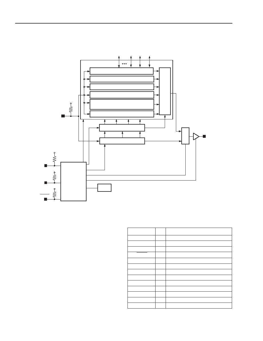
44
Lattice Semiconductor
Data Sheet
March, 2003
ORCA
Series 4 FPGAs
Special Function Blocks
(continued)
5-5768(F).b
Figure 27. ORCA Series Boundary-Scan Circuitry Functional Diagram
TAP
CONTROLLER
TMS
TCK
BOUNDARY-SCAN REGISTER
ISC READ/WRITE REGISTERS
BYPASS AND ISC_DEFAULT REGISTER
DATA
MUX
INSTRUCTION DECODER
INSTRUCTION REGISTER
M
U
X
RESET
CLOCK IR
SHIFT-IR
UPDATE-IR
PUR
TDO
SELECT
ENABLE
RESET
CLOCK DR
SHIFT-DR
UPDATE-DR
TDI
DATA REGISTERS
PSR1,PSR2,PSR3 REGISTERS (PLCs)
CONFIGURATION REGISTER
(RAM_R, RAM_W)
PRGM
I/O BUFFERS
V
DD
V
DD
V
DD
V
DD
IDCODE/USER CODE REGISTER
ORCA
Series TAP Controller (TAPC)
The ORCA Series TAP controller (TAPC) is a 1149
compatible test access port controller. The 16 JTAG
state assignments from the IEEE 1149 specification
are used. The TAPC is controlled by TCK and TMS. The
TAPC states are used for loading the IR to allow three
basic functions in testing: providing test stimuli
(Update-DR), test execution (Run-Test/Idle), and
obtaining test responses (Capture-DR). The TAPC
allows the test host to shift in and out both instructions
and test data/results. The inputs and outputs of the
TAPC are provided in the table below. The outputs are
primarily the control signals to the instruction register
and the data register.
Table 20. TAP Controller Input/Outputs
Symbol
I/O
Function
TMS
I
Test Mode Select
TCK
I
Test Clock
PUR
I
Powerup Reset
PRGM
I
BSCAN Reset
TRESET
O Test Logic Reset
Select
O Select IR (High); Select-DR (Low)
Enable
O Test Data Out Enable
Capture-DR
O Capture/Parallel Load-DR
Capture-IR
O Capture/Parallel Load-IR
Shift-DR
O Shift Data Register
Shift-IR
O Shift Instruction Register
Update-DR
O Update/Parallel Load-DR
Update-IR
O Update/Parallel Load-IR
Data Sheet
March, 2003
Lattice Semiconductor
45
ORCA
Series 4 FPGAs
Special Function Blocks
(continued)
The TAPC generates control signals that allow capture, shift, and update operations on the instruction and data
registers. In the capture operation, data is loaded into the register. In the shift operation, the captured data is
shifted out while new data is shifted in. In the update operation, either the instruction register is loaded for instruc-
tion decode, or the boundary-scan register is updated for control of outputs.
The test host generates a test by providing input into the ORCA Series TMS input synchronous with TCK. This
sequences the TAPC through states in order to perform the desired function on the instruction register or a data
register. Figure 28 provides a diagram of the state transitions for the TAPC. The next state is determined by the
TMS input value.
5-5370(F)
Figure 28. TAP Controller State Transition Diagram
SELECT-
DR-SCAN
CAPTURE-DR
SHIFT-DR
EXIT1-DR
PAUSE-DR
EXIT2-DR
UPDATE-DR
1
1
0
0
1
0
RUN-TEST/
IDLE
1
TEST-LOGIC-
RESET
SELECT-
IR-SCAN
CAPTURE-IR
SHIFT-IR
EXIT1-IR
PAUSE-IR
EXIT2-IR
UPDATE-IR
1
1
0
1
0
0
0
0
0
1
0
1
1
1
0
1
1
0
0
0
0
1
1
1
0
Boundary-Scan Cells
Figure 29 is a diagram of the boundary-scan cell (BSC)
in the ORCA series PIOs. There are four BSCs in each
PIC: one for each pad, except as noted above. The
BSCs are connected serially to form the BSR. The BSC
controls the functionality of the in, out, and 3-state sig-
nals for each I/O pad.
The BSC allows the I/O to function in either the normal
or test mode. Normal mode is defined as when an out-
put buffer receives input from the PLC array and pro-
vides output at the pad or when an input buffer
provides input from the pad to the PLC array. In the test
mode, the BSC executes a boundary-scan operation,
such as shifting in scan data from an upstream BSC in
the BSR, providing test stimuli to the pad, capturing
test data at the pad, etc.
The primary functions of the BSC are shifting scan data
serially in the BSR and observing input (p_in), output
(p_out), and 3-state (p_ts) signals at the pads. The
BSC consists of three circuits: the bidirectional data
cell is used to access the input and output data, the
capture cell is used to capture the status of the I/O pad,
and the direction control cell is used to access the 3-
state value. All three cells consist of a FF used to shift
scan data which feeds a FF to control the I/O buffer.
The capture cell is connected serially to the bidirec-
tional data cell, which is connected serially to the direc-
tion control cell to form a boundary-scan shift register.
The TAPC signals (capture, update, shiftn, treset, and
TCK) and the MODE signal control the operation of the
BSC. The bidirectional data cell is also controlled by
the high out/low in (HOLI) signal generated by the
direction control cell. When HOLI is low, the bidirec-
tional data cell receives input buffer data into the BSC.
When HOLI is high, the BSC is loaded with functional
data from the PLC.
46
Lattice Semiconductor
Data Sheet
March, 2003
ORCA
Series 4 FPGAs
Special Function Blocks
(continued)
The MODE signal is generated from the decode of the instruction register. When the MODE signal is high
(EXTEST), the scan data is propagated to the output buffer. When the MODE signal is low (BYPASS or SAMPLE),
functional data from the FPGA's internal logic is propagated to the output buffer.
The boundary-scan description language (BSDL) is provided for each device in the ORCA Series of FPGAs on the
ispLEVER CD. The BSDL is generated from a device profile, pinout, and other boundary-scan information.
5-2844(F).a
Figure 29. Boundary-Scan Cell
Boundary-Scan Timing
To ensure race-free operation, data changes on specific clock edges. The TMS and TDI inputs are clocked in on the
rising edge of TCK, while changes on TDO occur on the falling edge of TCK. In the execution of an EXTEST
instruction, parallel data is output from the BSR to the FPGA pads on the falling edge of TCK. The maximum fre-
quency allowed for TCK is 20 MHz.
Figure 30 shows timing waveforms for an instruction scan operation. The diagram shows the use of TMS to
sequence the TAPC through states. The test host (or BSM) changes data on the falling edge of TCK, and it is
clocked into the DUT on the rising edge.
D
Q
D
Q
D
Q
D
Q
P_OUT
HOLI
BIDIRECTIONAL DATA CELL
I/O BUFFER
DIRECTION CONTROL CELL
MODE
UPDATE/TCK
SCAN OUT
TCK
SHIFTN/CAPTURE
P_TS
P_IN
PAD_IN
PAD_TS
PAD_OUT
0
1
0
1
0
1
0
1
0
1
D
Q
D
Q
SCAN IN
0
1
CAPTURE CELL
INBS (TO FPGA ARRAY)
Data Sheet
March, 2003
Lattice Semiconductor
47
ORCA
Series 4 FPGAs
Special Function Blocks
(continued)
5-5971(F)
Figure 30. Instruction Register Scan Timing Diagram
TCK
TMS
TDI
RUN-TEST/IDLE
RUN-TEST/IDLE
EXIT1-IR
EXIT2-IR
UPDATE-IR
SELECT-DR-SCAN
CAPTURE-IR
SELECT-IR-SCAN
TEST-LOGIC-RESET
SHIFT-IR
PAUSE-IR
SHIFT-IR
EXIT1-IR
Single Function Blocks
Most of the special function blocks perform a specific
dedicated function. These functions are data/configura-
tion readback control, global 3-state control (TS_ALL),
internal oscillator generation, GSRN, and start-up
logic.
Readback Logic
The readback logic can be enabled via a bit stream
option or by instantiation of a library readback compo-
nent.
Readback is used to read back the configuration data
and, optionally, the state of the PFU outputs. A read-
back operation can be done while the FPGA is in nor-
mal system operation. The readback operation cannot
be daisy-chained. To use readback, the user selects
options in the bit stream generator in the ispLEVER
development system.
Table 21 provides readback options selected in the bit
stream generator tool. The table provides the number
of times that the configuration data can be read back.
This is intended primarily to give the user control over
the security of the FPGA's configuration program. The
user can prohibit readback (0), allow a single readback
(1), or allow unrestricted readback (U).
Table 21. Readback Options
Readback can be performed via the Series 4
MPI
or by
using dedicated FPGA readback controls. If the
MPI
is
enabled, readback via the dedicated FPGA readback
logic is disabled. Readback using the
MPI
is discussed
in the
MPI
section.
The pins used for dedicated readback are readback
data (RD_DATA), read configuration (
RD_CFG
), and
configuration clock (CCLK). A readback operation is
initiated by a high-to-low transition on
RD_CFG
. The
RD_CFG
input must remain low during the readback
operation. The readback operation can be restarted at
frame 0 by driving the
RD_CFG
pin high, applying at
least two rising edges of CCLK, and then driving
RD_CFG
low again. One bit of data is shifted out on
RD_DATA at the rising edge of CCLK. The first start bit
of the readback frame is transmitted out several cycles
after the first rising edge of CCLK after
RD_CFG
is input
low (see the readback timing characteristics table in the
timing characteristics section). To be certain of the start
of the readback frame, the data can be monitored for
the 01 frame start bit pair.
Option
Function
0
Prohibit Readback
1
Allow One Readback Only
U
Allow Unrestricted Number of Readbacks

48
48
Lattice Semiconductor
Data Sheet
March, 2003
ORCA
Series 4 FPGAs
Special Function Blocks
(continued)
Readback can be initiated at an address other than
frame 0 via the new
MPI
control registers (see the
MP
I
section for more information). In all cases, readback is
performed at sequential addresses from the start
address.
It should be noted that the RD_DATA output pin is also
used as the dedicated boundary-scan output pin, TDO.
If this pin is being used as TDO, the RD_DATA output
from readback can be routed internally to any other pin
desired. The
RD_CFG
input pin is also used to control
the global 3-state (TS_ALL) function. Before and during
configuration, the TS_ALL signal is always driven by
the
RD_CFG
input and readback is disabled. After con-
figuration, the selection as to whether this input drives
the readback or global 3-state function is determined
by a set of bit stream options. If used as the
RD_CFG
input for readback, the internal TS_ALL input can be
routed internally to be driven by any input pin.
The readback frame contains the configuration data
and the state of the internal logic. During readback, the
value of all registered PFU and PIO outputs can be
captured. The following options are allowed when
doing a capture of the PFU outputs.
Do not capture data (the data written to the RAMs,
usually 0, will be read back).
Capture data upon entering readback.
Capture data based upon a configurable signal inter-
nal to the FPGA. If this signal is tied to logic 0, cap-
ture RAMs are written continuously.
Capture data on either options two or three above.
The readback frame has an identical format to that of
the configuration data frame, which is discussed later
in the Configuration Data Format section. If LUT mem-
ory is not used as RAM and there is no data capture,
the readback data (not just the format) will be identical
to the configuration data for the same frame. This
eases a bitwise comparison between the configuration
and readback data. The configuration header, including
the length count field, is not part of the readback frame.
The readback frame contains bits in locations not used
in the configuration. These locations need to be
masked out when comparing the configuration and
readback frames. The development system optionally
provides a readback bit stream to compare to readback
data from the FPGA. Also note that if any of the LUTs
are used as RAM and new data is written to them,
these bits will not have the same values as the original
configuration data frame either.
Global 3-State Control (TS_ALL)
To increase the testability of the ORCA Series FPGAs,
the global 3-state function (TS_ALL) disables the
device. The TS_ALL signal is driven from either an
external pin or an internal signal. Before and during
configuration, the TS_ALL signal is driven by the input
pad
RD_CFG
. After configuration, the TS_ALL signal
can be disabled, driven from the
RD_CFG
input pad, or
driven by a general routing signal in the upper right cor-
ner. Before configuration, TS_ALL is active-low; after
configuration, the sense of TS_ALL can be inverted.
The following occur when TS_ALL is activated:
All of the user I/O output buffers are 3-stated, the
user I/O input buffers are pulled up (with the pull-
down disabled), and the input buffers are configured
with TTL input thresholds.
The TDO/RD_DATA output buffer is 3-stated.
The RD_CFG, RESET, and PRGM input buffers
remain active with a pull-up.
The DONE output buffer is 3-stated, and the input
buffer is pulled up.

Lattice Semiconductor
49
Data Sheet
March, 2003
ORCA
Series 4 FPGAs
Microprocessor Interface (MPI)
The Series 4 FPGAs have a dedicated synchronous
MPI function block. The MPI is programmable to oper-
ate with PowerPC/PowerQUICC MPC860/MPC8260
series microprocessors. The MPI implements an 8-,
16-, or 32-bit interface with 1-bit, 2-bit, or 4-bit parity to
the host processor (PowerPC) that can be used for
configuration and readback of the FPGA as well as for
user-defined data processing and general monitoring
of FPGA functions. In addition to dedicated-function
registers, the MPI bridges to the AMBA embedded sys-
tem bus through which the PowerPC bus master can
access the FPGA configuration logic, EBR and other
user logic. There is also capability to interrupt the host
processor either by a hard interrupt or by having the
host processor poll the MPI and the embedded system
bus.
The control portion of the MPI is available following
powerup of the FPGA if the mode pins specify MPI
mode, even if the FPGA is not yet configured. The
width of the data port is selectable among 8-, 16-, or
32-bit and the parity bus can be 1-, 2-, or 4-bit. In con-
figuration mode the data and parity bus width are
related to the state of the M[0:3] mode pins. For post-
configuration use, the MPI must be included in the con-
figuration bit stream by using an MPI library element in
your design from the ORCA macro library, or by setting
the bit of the MPI configuration control register prior to
the start of configuration. The user can also enable and
disable the parity bus through the configuration bit
stream. These pads can be used as general I/O when
they are not needed for MPI use.
Table 22 shows the interface signals that are used to
interface Series 4 devices to a PowerPC MPC860/
MPC8260 device. More information is available in the
Series 4 MPI and System Bus application note.
The ORCA FPGA is a memory-mapped peripheral to
the PowerPC processor. The MPI interfaces to the
user-programmable FPGA logic using the AMBA
embedded system bus.The MPI has access to a series
of addressable registers made accessible by the AMBA
system bus that provide MPI control and status, config-
uration and readback data transfer, FPGA device iden-
tification, and a dedicated user scratchpad register. All
registers are 8 bits wide. The address map for these
registers and the user-logic address space utilize the
same registers as the AMBA embedded system bus.
Embedded System Bus (ESB)
Implemented using the open standard, on-chip AMBA-
AHB 2.0 specification bus, the Series 4 devices con-
nects all the FPGA elements together with a standard-
ized bus framework. The ESB facilitates
communication among MPI, configuration, EBRs, and
user logic in all the generic FPGA devices. AHB serves
the need for high-performance
system-on-chip
(SoC) as well as aligning with current synthesis design
flows. Multiple bus masters optimizes system perfor-
mance by sharing resources between different bus
masters such as the MPI and configuration logic. The
wide data bus configuration of 32-bits with 4-bit parity
supports the high-bandwidth of data-intensive applica-
tions of using the wide on-chip memory. AMBA
enhances a reusable design methodology by defining a
common backbone for IP modules.
The ESB is a synchronous bus that is driven by either
the MPI clock, internal oscillator, CCLK (slave configu-
ration modes), TCK (JTAG configuration modes), or by
a user clock from routing. In FPSCs, a clock from the
embedded block can also drive the MPI clock. During
initial configuration and reconfiguration the bus clock is
defaulted to the configuration clock. The post configu-
ration clock source is set during configuration. The user
has the ability to program several slaves through the
user logic interface. Embedded block RAM also inter-
faces seamlessly to the system bus.
A single bus arbiter controls the traffic on the bus by
ensuring only one master has access to the bus at any
time. The arbiter monitors a number of different
requests to use the bus and decides which request is
currently the highest priority. The configuration modes
have the highest priority and overrides all normal user
modes. Priority can be programmed between MPI and
user logic at configuration in generic FPGAs. If no pri-
ority is set a round-robin approach is used by granting
the next requesting master in a rotating fixed order.
Several interfaces exist between the ESB and other
FPGA elements. The MPI interface acts as a bridge
between the external microprocessor bus and ESB.
The MPI may work in an independent clock domain
from the ESB if the ESB clock is not sourced from the
external microprocessor clock. Pipelined operation
allows high-speed memory interface to the EBR and
peripheral access without the requirement for addi-
tional cycles on the bus. Burst transfers allow optimal
use of the memory interface by giving advance infor-
mation of the nature of the transfers.
Table 23 is a listing of the ESB register file and brief
descriptions. Table 24 shows the system interrupt reg-
isters and Table 25 and Table 26 show the FPGA status
and command registers, all with brief descriptions.
More information is available in the Series 4 MPI and
System Bus application note.
50
Lattice Semiconductor
Data Sheet
March, 2003
ORCA
Series 4 FPGAs
Microprocessor Interface
(continued)
Table 22. MPC 860 to ORCA MPI Interconnection
PowerPC
Signal
ORCA
Pin
Name
MPI
I/O
Function
D[0:n]
D[0:n]
I/O
8, 16, 32-bit data bus.
DP[0:m]
DP[0:m]
I/O
Selectable parity bus width from1, 2, and 4-bit.
A[14:31]
PPC_A[14:31]
I
32-bit MPI address bus.
TS
MPI_STRB
I
Transfer start signal.
BURST
MPI_BURST
I
Active-low indicates burst transfer in-progress. High indicates current transfer
not a burst.
--
CS0
I
Active-low MPI select.
--
CS1
I
Active-high MPI select.
CLKOUT
MPI_CLK
I
PowerPC
interface clock.
RD/WR
MPI_RW
I
Read (high)/write (low) signal.
TA
MPI_ACK
O
Active-low transfer acknowledge signal.
BDIP
MPI_BDIP
I
Active-low burst transfer in progress signal indicates that the second beat in
front of the current one is requested by the master. Negated before the burst
transfer ends to abort the burst data phase.
Any of
IRQ[7:0]
MPI_IRQ
O
Active-low interrupt request signal.
TEA
MPI_TEA
O
Active-low indicates MPI detects a bus error on the internal system bus for
current transaction.
RETRY
MPI_RTRY
O
Requests the MPC860/MPC8260 to relinquish the bus and retry the cycle.
TSZ[0:1]
MPI_TSZ[0:1]
I
Driven to indicate the data transfer size for the transaction (byte, half-word,
word).
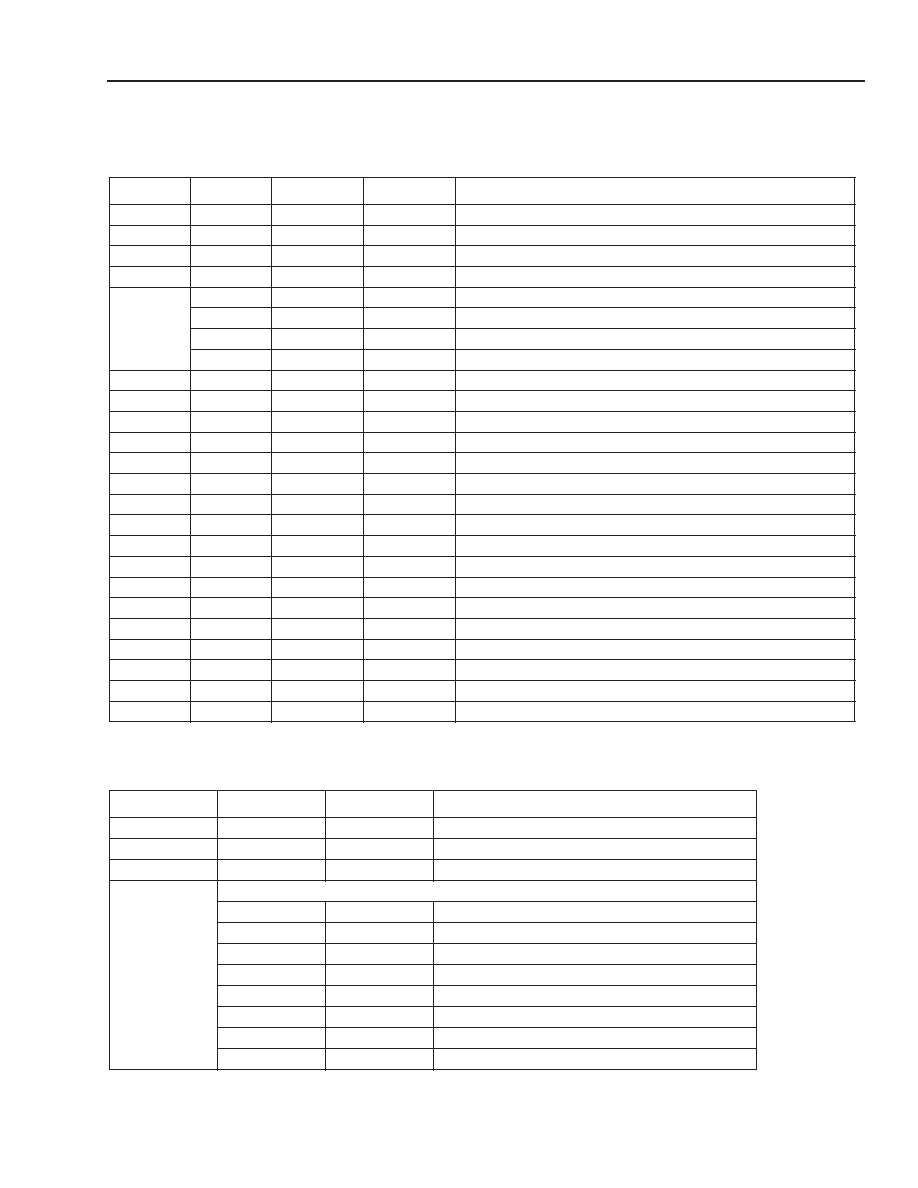
Lattice Semiconductor
51
Data Sheet
March, 2003
ORCA
Series 4 FPGAs
Microprocessor Interface
(continued)
Table 23. Embedded System Bus/MPI Registers
Note: RO = Read Only, R/W = Read/Write
Table 24. Interrupt Register Space Assignments
Note: RO = Read Only, R/W = Read/Write.
For internal system bus, bit 7 is most significant bit, for MPI bit 0 is most significant bit.
Register
Byte
Read/Write Initial Value
Description
00
03-00
RO
--
32-bit device ID
01
07-04
R/W
--
Scratchpad register
02
0B-08
R/W
--
Command register
03
0F-0C
RO
--
Status register
04
13
R/W
--
Interrupt enable register � MPI
12
R/W
--
Interrupt enable register � USER
11
R/W
--
Interrupt enable register � FPSC (unused for FPGAs)
10
RO
--
Interrupt cause register
05
17-14
R/W
--
Readback address register (14 bits)
06
1B-18
RO
--
Readback data register
07
1F-1C
R/W
--
Configuration data register
08
23-20
RO
--
Trap address register
09
27-24
RO
--
Bus error address register
0A
2B-28
RO
--
Interrupt vector 1 predefined by configuration bit stream
0B
2F-2C
RO
--
Interrupt vector 2 predefined by configuration bit stream
0C
33-30
RO
--
Interrupt vector 3 predefined by configuration bit stream
0D
37-34
RO
--
Interrupt vector 4 predefined by configuration bit stream
0E
3B-38
RO
--
Interrupt vector 5 predefined by configuration bit stream
0F
3F-3C
RO
--
Interrupt vector 6 predefined by configuration bit stream
10
43--40
--
--
Top-left PPLL
11
47--44
--
--
Top-left HPLL
14
53--50
--
--
Top-right PPLL
18
63--60
--
--
Bottom-left PPLL
19
67--64
--
--
Bottom-left HPLL
1C
73--70
--
--
Bottom-right PPLL
Byte
bit
Read/Write
Description
13
7-0
R/W
Interrupt Enable Register � MPI
12
7-0
R/W
Interrupt Enable Register � USER
11
7-0
R/W
Interrupt Enable Register � FPSC
10
Interrupt Cause Registers
7
RO
USER_IRQ_GENERAL;
6
RO
USER_IRQ_SLAVE;
5
RO
USER_IRQ_MASTER;
4
RO
CFG_IRQ_DATA;
3
RO
ERR_FLAG 1
2
RO
MPI_IRQ
1
RO
FPSC_IRQ_SLAVE;
0
RO
FPSC_IRQ_MASTER

52
Lattice Semiconductor
Data Sheet
March, 2003
ORCA
Series 4 FPGAs
Microprocessor Interface
(continued)
Table 25. Status Register Space Assignments
Notes: RO = Read Only. For internal system bus, bit 7 is most significant bit, for MPI bit 0 is most significant bit.
Table 26. Command Register Space Assignments
Note: R/W = Read/Write. For internal system bus; bit 7 is most significant bit, for MPI bit 0 is most significant bit.
Byte
bit
Read/Write
Description
0F
7:0
--
Reserved
0E
7:0
--
Reserved
OD
7
RO
Configuration Write Data Acknowledge
6
RO
Readback Data Ready
5
RO
Unassigned (Zero)
4
RO
Unassigned (Zero)
3
RO
FPSC_BIT_ERR
2
RO
RAM_BIT_ERR
1
RO
Configuration Write Data Size (1, 2, or 4 bytes)
0
RO
Use with above for HSIZE[1:0] (byte, half-word, word)
0C
7
RO
Readback Addresses Out of Range
6
RO
Error Response Received by CFG From System Bus
5
RO
Error Responses Received by CFG From System Bus
4
RO
CFG_DATA_LOST
3
RO
DONE
2
RO
INIT_N
1
RO
ERR_FLAG 1
0
RO
ERR_FLAG 0
Byte
bit
Read/Write
Description
0B
7:0
--
Reserved
0A
7:0
--
Reserved
09
7
R/W
SYS_GSR (GSR Input)
6
R/W
SYS_RD_CFG (similar to FPGA pin RD_CFGN, but active high)
5
R/W
PRGM from MPI > (similar to FPGA pin, but active high)
4
R/W
PRGM from USER > (similar to FPGA pin, but active high)
3
R/W
PRGM from FPSC > (similar to FPGA pin, but active high)
2
R/W
LOCK from MPI
1
R/W
LOCK from USER
0
R/W
LOCK from FPSC
08
7
R/W
Bus Reset from MPI (resets system bus and registers)
6
R/W
Bus Reset from USER (resets system bus and registers)
5
R/W
Bus Reset from FPSC (resets system bus and registers)
4
R/W
SYS_DAISY
3
R/W
REPEAT_RDBK (don't increment readback address)
2
R/W
MPI_USR_ENABLE
1
R/W
Readback Data Size (1, 2, or 4 bytes)
0
R/W
Use with above for HSIZE[1:0]
Lattice Semiconductor
53
Data Sheet
March, 2003
ORCA
Series 4 FPGAs
Phase-Locked Loops (PLLs)
There are eight PLLs available to perform many clock modification and clock conditioning functions on the Series 4
FPGAs. Six of the PLLs are programmable allowing the user the flexibility to configure the PLL to manipulate the
frequency, phase, and duty cycle of a clock signal. Four of the programmable PLLs (PPLLs) are capable of manipu-
lating and conditioning clocks from 15 MHz to 200 MHz and two others (HPPLLs) are capable of manipulating and
conditioning clocks from 60 MHz to 420 MHz. Frequencies can be adjusted from 1/64x to 64x the input clock fre-
quency. Each programmable PLL provides two outputs that have different multiplication factors with the same
phase relationships. Duty cycles and phase delays can be adjusted in 12.5% of the clock period increments. An
automatic delay compensation mode is available for phase delay. Each PPLL and HPPLL provides two outputs that
can have programmable (45 degree increments) phase differences.
The PPLLs and HPPLLs can be utilized to eliminate skew between the clock input pad and the internal clock inputs
across the entire device. Both the PPLLS or the HPPLLs can drive onto the primary and secondary clock networks
inside the FPGA. Each can take a clock input from the dedicated pad or differential pair of pads in its corner or from
general routing resources.
Functionality of the PPLLs and HPPLLs is programmed during operation through a control register internal to the
FPGA array or via the configuration bit stream. The embedded system bus enables access to these registers (see
Table 23). There is also a PLL output signal, LOCK, that indicates a stable output clock state.
Table 27. PPLL Specifications
Additional highly tuned and characterized dedicated phase-locked loops (DPLLs) are included to ease system
designs. These DPLLs meet ITU-T G.811 primary clocking specifications and enable system designers to target
very tightly specified clock conditioning not available in the programmable PPLLs. They also provide enhanced jitter
filtering to reduce the amount of input jitter that is transferred to the PLL output when used in any application.
DPLLs are targeted to low-speed DS1 and E1 networking systems (PLL1) and high-speed SONET/SDH network-
ing STS-3 and STM-1 networking systems (PLL2).
Parameter
Min
Nom
Max
Unit
V
DD
15
1.425
1.5
1.575
V
V
DD
33
3.0
3.3
3.6
V
Operating Temp
�40
--
125
C
Input Clock Frequency
(No division)
PPLL
2.0
--
200
MHz
HPPLL
7.5
--
420
Output Clock Frequency
PPLL
15
--
200
MHz
HPPLL
60
--
420
Input Duty Cycle
30
--
70
%
Output Duty Cycle
45
50
55
%
Lock Time
--
<50
--
�s
Frequency Multiplication
Up to 64x
--
Frequency Division
Down to 1/64x
--
Duty Cycle Adjust of Output Clock
12.5, 25, 37.5, 50, 62.5, 75, 87.5
%
Delay Adjust of Output Clock
0, 45, 90, 135, 180, 225, 270, 315
degrees
Phase Shift Between MCLK and NCLK
0, 45, 90, 135, 180, 225, 270, 315
degrees
54
Lattice Semiconductor
Data Sheet
March, 2003
ORCA
Series 4 FPGAs
Phase-Locked Loops
(continued)
Table 28. DS-1/E-1 PLL1 Specifications
A dedicated pin PLL_VF is needed for externally connecting a low pass filter circuit.
This provides the specified DS�1/E�1 PLL operating condition.
0203(F).
Figure 31. PLL_VF External Requirements
Parameter
Min
Nom
Max
Unit
V
DD
15
1.425
1.5
1.575
V
V
DD
33
3.0
3.3
3.6
V
Operating Temp
�40
--
125
C
Input Clock Frequency
1.0
--
2.5
MHz
Output Clock Frequency
1.0
--
2.5
MHz
Input Duty Cycle
30
--
70
%
Output Duty Cycle
47
50
53
%
Lock Time
--
<1200
--
�s
PLL_VF
C
1
C
2
R
1
R
1
= 6 k
� 1%
C
1
= 100 pF
� 5%
C
2 =
0.01
�
F � 5%
V
SS
Lattice Semiconductor
55
Data Sheet
March, 2003
ORCA
Series 4 FPGAs
Phase-Locked Loops
(continued)
Table 29. STS-3/STM-1 PLL2 Specifications
All Series 4 PLLs operate from the V
DD
33 power supply. Care needs to be taken during board layout to properly iso-
late and filter this power supply. More information about the PLLs is available in the Series 4 FPGA PLL Elements
application note. The location of all eight PLLs on Series 4 FPGAs is shown in Figure 32 and Table 30.
0045(F)
Figure 32. PLL Naming Scheme
Table 30. Phase-lock Loops Index
Parameter
Min
Nom
Max
Unit
V
DD
15
1.425
1.5
1.575
V
V
DD
33
3.0
3.3
3.6
V
Operating Temp
�40
--
125
C
Input Clock Frequency
140
155.52
170
MHz
Output Clock Frequency
140
155.52
170
MHz
Input Duty Cycle Tolerance
30
--
70
%
Output Duty Cycle
47
50
53
%
Lock Time
--
<50
--
�s
Name Description
[UL][LL][UR][LR]PPLL
Universal user programmable PLL (15--200 MHz)
[UL][LL]HPPLL
Universal user programmable PLL (60--420 MHz)
URPLL1
DS-1/E-1 dedicated PLL
LRPLL2
STS-1/STM-1 dedicated PLL
LRPPLL LRPLL2
LLPPLL LLHPPLL
URPPLL URPLL1
ULPPLL ULHPPLL
56
56
Lattice Semiconductor
Data Sheet
March, 2003
ORCA
Series 4 FPGAs
FPGA States of Operation
Prior to becoming operational, the FPGA goes through
a sequence of states, including initialization, configura-
tion, and start-up. Figure 33 outlines these three states.
5-4529(F).
Figure 33. FPGA States of Operation
Initialization
Upon powerup, the device goes through an initialization
process. First, an internal power-on-reset circuit is trig-
gered when power is applied. When V
DD
15 and V
DD
33
reach the voltage at which portions of the FPGA begin
to operate, the I/Os are configured based on the config-
uration mode, as determined by the mode select inputs
M[3:0]. A time-out delay is then initiated to allow the
power supply voltage to stabilize. The
INIT
and DONE
outputs are low.
At the end of initialization, the default configuration
option is that the configuration RAM is written to a low
state. This prevents internal shorts prior to configura-
tion. As a configuration option, after the first configura-
tion (i.e., at reconfiguration), the user can reconfigure
without clearing the internal configuration RAM first.
The active-low, open-drain initialization signal
INIT
is
released and must be pulled high by an external resis-
tor when initialization is complete. To synchronize the
configuration of multiple FPGAs, one or more
INIT
pins
should be wire-ANDed. If
INIT
is held low by one or
more FPGAs or an external device, the FPGA remains
in the initialization state.
INIT
can be used to signal that
the FPGAs are not yet initialized. After
INIT
goes high
for two internal clock cycles, the mode lines (M[3:0])
are sampled, and the FPGA enters the configuration
state.
The high during configuration (HDC), low during config-
uration (
LDC
), and DONE signals are active outputs in
the FPGA's initialization and configuration states. HDC,
LDC
, and DONE can be used to provide control of
external logic signals such as reset, bus enable, or
PROM enable during configuration. For parallel master
configuration modes, these signals provide PROM
enable control and allow the data pins to be shared
with user logic signals.
If configuration has begun, an assertion of
RESET
or
PRGM
initiates an abort, returning the FPGA to the ini-
tialization state. The
PRGM
and
RESET
pins must be
pulled back high before the FPGA will enter the config-
uration state. During the start-up and operating states,
only the assertion of
PRGM
causes a reconfiguration.
In the master configuration modes, the FPGA is the
source of configuration clock (CCLK). In this mode, the
initialization state is extended to ensure that, in daisy-
chain operation, all daisy-chained slave devices are
ready. Independent of differences in clock rates, master
mode devices remain in the initialization state an addi-
tional six internal clock cycles after
INIT
goes high.
When configuration is initiated, a counter in the FPGA
is set to 0 and begins to count configuration clock
cycles applied to the FPGA. As each configuration data
frame is supplied to the FPGA, it is internally assem-
bled into data words. Each data word is loaded into the
internal configuration memory. The configuration load-
ing process is complete when the internal length count
equals the loaded length count in the length count field,
and the required end of configuration frame is written.
During configuration, the PIO and PLC latches/FFs are
held set/reset and the internal SLIC buffers are
3-stated. The combinatorial logic begins to function as
the FPGA is configured. Figure 34 shows the general
waveform of the initialization, configuration, and start-
up states.
� ACTIVE I/O
� RELEASE INTERNAL RESET
� DONE GOES HIGH
START-UP
INITIALIZATION
CONFIGURATION
RESET
OR
PRGM
LOW
PRGM
LOW
� CLEAR CONFIGURATION MEMORY
� INIT LOW, HDC HIGH, LDC LOW
OPERATION
POWERUP
� POWER-ON TIME DELAY
� M[3:0] MODE IS SELECTED
� CONFIGURATION DATA FRAME WRITTEN
� INIT HIGH, HDC HIGH, LDC LOW
� DOUT ACTIVE
YES
NO
NO
RESET,
INIT,
OR
PRGM
LOW
BIT
ERROR
YES

Lattice Semiconductor
57
Data Sheet
March, 2003
ORCA
Series 4 FPGAs
FPGA States of Operation
(continued)
Power Supply Sequencing
FPGAs are CMOS static RAM (SRAM) based program-
mable logic devices. The circuitry that the user designs
for the FPGA is implemented within the FPGA by set-
ting multiple SRAM configuration memory cells. This
unique structure as compared with typical CMOS cir-
cuits lends to having certain powerup voltage and cur-
rent requirements. This section describes these related
power issues for the ORCA Series 4 FPGAs and
FPSCs.
The flexibility of Series 4 FPGAs lends itself to more
power up considerations as it mixes many power sup-
plies to meet today's versatile system standards. The
board designer must account for the relationship of the
supplies early in board development. The proper
sequence of supplies insures that the board will not be
troubled with power up issues.
The Series 4 devices have many new design improve-
ments to prevent short-circuit contention. This conten-
tion is typically caused by configuration RAM cells in
the device not all powering up to a Q = 0 RAM state. In
order for this to occur, a minimum current was needed
to push the internal circuitry beyond the initial short-cir-
cuit-like condition to become a full CMOS circuit.
Series 4 has overcome this requirement through many
improvements which have dramatically decreased the
adverse effects of internal power up memory conten-
tion.
At power up, the internal V
DD
ramp and the duration of
the ramp will depend on the amount of dynamic current
available from the power supply. If a large amount of
current is available, the voltage ramp seen by the
device will be very fast. When final voltage has been
reached, this high quiescent current is no longer
required. If the available current is limited, the time for
the device power to rise will be longer. The voltage
ramp should be monotonic with very little or no flatten-
ing as the supply ramps up. It is also recommended
that the supply should not rise and fall as it is powering
up as this will cause improper power up behavior.
In Series 4 devices, it is recommended that the V
DD
15
supply pass through its operational threshold voltage of
approximately 1 V before the V
DD
33 supply reaches its
operational threshold of 2.3 V. The current required by
both V
DD
15 and V
DD
33 supplies while it passes
through their operational thresholds is approximately
between 1 and 2 amperes each. The powering of the
V
DD
IO supplies should be after the V
DD
15 and V
DD
33
supplies reach operational levels. This sequence and
supply currents can guarantee that the device will prop-
erly power up without any adverse effects.
In cases where the power up ramps are greater than 50
mS, it is recommended that PRGM pin be held low dur-
ing power up. However, this work around is only valid if
the power supplies meet the above mentioned current
and voltage requirements. The assertion of the PRGM
will hold off the device from configuration while the
device stabilizes and will not counter act any internal
power up requirements.
Configuration
The ORCA Series FPGA functionality is determined by
the state of internal configuration RAM. This configura-
tion RAM can be loaded in a number of different
modes. In these configuration modes, the FPGA can
act as a master or a slave of other devices in the sys-
tem. The decision as to which configuration mode to
use is a system design issue. Configuration is dis-
cussed in detail, including the configuration data format
and the configuration modes used to load the configu-
ration data in the FPGA, following a description of the
start-up state.
Start-Up
After configuration, the FPGA enters the start-up
phase. This phase is the transition between the config-
uration and operational states and begins when the
number of CCLKs received after
INIT
goes high is
equal to the value of the length count field in the config-
uration frame and when the end of configuration frame
has been written. The system design issue in the start-
up phase is to ensure the user I/Os become active
without inadvertently activating devices in the system
or causing bus contention. A second system design
concern is the timing of the release of global set/reset
of the PLC latches/FFs.

58
Lattice Semiconductor
Data Sheet
March, 2003
ORCA
Series 4 FPGAs
FPGA States of Operation
(continued)
5-4482(F)
Figure 34. Initialization/Configuration/Start-Up Waveforms
INITIALIZATION
CONFIGURATION
START-UP
OPERATION
V
DD
15, V
DD
33
RESET
PRGM
INIT
M[3:0]
CCLK
HDC
LDC
DONE
USER I/O
INTERNAL
RESET
(gsm)

Lattice Semiconductor
59
Data Sheet
March, 2003
ORCA
Series 4 FPGAs
FPGA States of Operation
(continued)
There are configuration options that control the relative
timing of three events: DONE going high, release of the
set/reset of internal FFs, and user I/Os becoming
active. Figure 35 shows the start-up timing for ORCA
FPGAs. The system designer determines the relative
timing of the I/Os becoming active, DONE going high,
and the release of the set/reset of internal FFs. In the
ORCA
Series FPGA, the three events can occur in any
arbitrary sequence. This means that they can occur
before or after each other, or they can occur simulta-
neously.
There are four main start-up modes: CCLK_NOSYNC,
CCLK_SYNC, UCLK_NOSYNC, and UCLK_SYNC.
The only difference between the modes starting with
CCLK and those starting with UCLK is that for the
UCLK modes, a user clock must be supplied to the
start-up logic. The timing of start-up events is then
based upon this user clock, rather than CCLK. The dif-
ference between the SYNC and NOSYNC modes is
that for SYNC mode, the timing of two of the start-up
events, release of the set/reset of internal FFs, and the
I/Os becoming active is triggered by the rise of the
external DONE pin followed by a variable number of
rising clock edges (either CCLK or UCLK). For the
NOSYNC mode, the timing of these two events is
based only on either CCLK or UCLK.
DONE is an open-drain bidirectional pin that may
include an optional (enabled by default) pull-up resistor
to accommodate wired ANDing. The open-drain DONE
signals from multiple FPGAs can be tied together
(ANDed) with a pull-up (internal or external) and used
as an active-high ready signal, an active-low PROM
enable, or a reset to other portions of the system.
When used in SYNC mode, these ANDed DONE pins
can be used to synchronize the other two start-up
events, since they can all be synchronized to the same
external signal. This signal will not rise until all FPGAs
release their DONE pins, allowing the signal to be
pulled high.
An example of using the synchronized modes are the
CCLK_SYNC synchronized start-up mode where
DONE is released on the first CCLK rising edge, C1
(see Figure 35).
Since this is a synchronized start-up mode, the open-
drain DONE signal can be held low externally to stop
the occurrence of the other two start-up events. Once
the DONE pin has been released and pulled up to a
high level, the other two start-up events can be pro-
grammed individually to either happen immediately or
after up to four rising edges of CCLK (Di, Di + 1, Di + 2,
Di + 3, Di + 4). The default is for both events to happen
immediately after DONE is released and pulled high.
A commonly used design technique is to release
DONE one or more clock cycles before allowing the I/O
to become active. This allows other configuration
devices, such as PROMs, to be disconnected using the
DONE signal so that there is no bus contention when
the I/Os become active. In addition to controlling the
FPGA during start-up, other start-up techniques that
avoid contention include using isolation devices
between the FPGA and other circuits in the system,
reassigning I/O locations, and maintaining I/Os as
3-stated outputs until contentions are resolved.
Each of these start-up options can be selected during
bit stream generation in ispLEVER, using Advanced
Options. For more information, please see the
ispLEVER documentation.

60
Lattice Semiconductor
Data Sheet
March, 2003
ORCA
Series 4 FPGAs
FPGA States of Operation
(continued)
5-2761(F)
Figure 35. Start-Up Waveforms
Di
C1
C2
C3
C4
F
C1
C2
C3
C4
C1
C2
C3
C4
C1, C2, C3, OR C4
Di + 1
Di
Di + 2
Di + 3
Di + 4
Di + 1
Di
Di + 2
Di + 3
Di + 4
ORCA
CCLK_SYNC
DONE IN
U1
U2
U3
U4
F
U1
U2
U3
U4
U1
U2
U3
U4
ORCA
UCLK_NOSYNC
Di
Di + 1
Di + 2
Di + 3
ORCA
UCLK_SYNC
UCLK PERIOD
SYNCHRONIZATION UNCERTAINTY
DONE IN
F
C1
C1
U1, U2, U3, OR U4
DONE
I/O
GSRN
ACTIVE
DONE
I/O
GSRN
ACTIVE
DONE
I/O
GSRN
ACTIVE
DONE
I/O
GSRN
ACTIVE
UCLK
F = FINISHED, NO MORE CLKS REQUIRED.
CCLK
F
ORCA
CCLK_NOSYNC
Di + 4
Di + 3
Di + 2
Di + 1
PERIOD

Lattice Semiconductor
61
Data Sheet
March, 2003
ORCA
Series 4 FPGAs
FPGA States of Operation
(continued)
Reconfiguration
To reconfigure the FPGA when the device is operating
in the system, a low pulse is input into
PRGM
or one of
the program bits in the embedded system bus control
register must be set. The configuration data in the
FPGA is cleared, and the I/Os not used for configura-
tion are 3-stated with a pullup. The FPGA then samples
the mode select inputs and begins reconfiguration.
When reconfiguration is complete, DONE is released,
allowing it to be pulled high.
Partial Reconfiguration
All ORCA device families have been designed to allow
a partial reconfiguration of the FPGA at any time. This
is done by setting a bit stream option in the previous
configuration sequence that tells the FPGA to not reset
all of the configuration RAM during a reconfiguration.
Then only the configuration frames that are to be modi-
fied need to be rewritten, thereby reducing the configu-
ration time.
Other bit stream options are also available that allow
one portion of the FPGA to remain in operation while a
partial reconfiguration is being done. If this is done, the
user must be careful to not cause contention between
the two configurations (the bit stream resident in the
FPGA and the partial reconfiguration bit stream) as the
second reconfiguration bit stream is being loaded.
During a partial re-configuration where the configura-
tion option is set to have the internal logic remain active
during configuration the internal SLJC BIDI signals will
always be 3-stated. Previous families of ORCA FPGAs
would allow the BIDIs to continue to be under user
logic control during a partial re-configuration.
Other Configuration Options
There are many other configuration options available to
the user that can be set during bit stream generation in
ispLEVER. These include options to enable boundary-
scan and/or the MPI and/or the programmable PLL
blocks, readback options, and options to control and
use the internal oscillator after configuration.
Other useful options that affect the next configuration
(not the current configuration process) include options
to disable the global set/reset during configuration, dis-
able the 3-state of I/Os during configuration, and dis-
able the reset of internal RAMs during configuration to
allow for partial configurations (see above). For more
information on how to set these and other configuration
options, please see the ispLEVER documentation.
Configuration Data Format
The ispLEVER Development System interfaces with
front-end design entry tools and provides tools to pro-
duce a fully configured FPGA. This section discusses
using the ispLEVER Development System to generate
configuration RAM data and then provides the details
of the configuration frame format.
Using ispLEVER to Generate Configuration
RAM Data
The configuration data bit stream defines the I/O func-
tionality, logic, and interconnections within the FPGA.
The bit stream is generated by the development sys-
tem. The bit stream created by the bit stream genera-
tion tool is a series of 1s and 0s used to write the FPGA
configuration RAM. It can be loaded into the FPGA
using one of the configuration modes discussed later.
In bit stream generator, the designer selects options
that affect the FPGA's functionality. Using the output of
the bit stream generator, circuit_name.bit, the devel-
opment system's download tool can load the configura-
tion data into the ORCA series FPGA evaluation board
from a PC or workstation.
A download cable that can be used to download from
any PC or workstation supported by ispLEVER is avail-
able. This cable allows download to an FPGA that can
be programmed via the serial configuration interface
(requiring the mode pins to be set) or the JTAG bound-
ary scan interface (not requiring the setting of mode
pins). The lead device can then program other FPGAs
or FPSCs on the board via daisy-chaining.
Alternatively, a user can program a PROM (such as a
Serial ROM or a standard EPROM) and load the FPGA
from the PROM. The development system's PROM
programming tool produces a file in .mcs, .tek or .exo
format.

62
Lattice Semiconductor
Data Sheet
March, 2003
ORCA
Series 4 FPGAs
Configuration Data Format
(continued)
Configuration Data Frame
Configuration data can be presented to the FPGA in two frame formats: autoincrement and explicit. A detailed
description of the frame formats is shown in Figure 36, Figure 37, and Tables Table 31 and Table 31A. The two
modes are similar except that autoincrement mode uses assumed address incrementation to reduce the bit stream
size, and explicit mode uses an optional address frame. In both cases, the header frame begins with a series of 1s
and a preamble of 0010, followed by a 24-bit length count field representing the total number of configuration
clocks needed to complete the loading of the FPGAs. If only Series 4 devices are used, a second preamble value
of 0100 is supported. If this preamble is found, the Series 4 device will expect an expanded length count field of 32-
bits. This allows more larger Series 4 FPGAs to be configured through daisy-chaining.
Following the header frame is a mandatory ID frame. The ID frame contains data used to determine if the bit
stream is being loaded to the correct type of ORCA FPGA (i.e., a bit stream generated for an OR4E06 is being sent
to an OR4E06). Error checking is always enabled for Series 4 devices through the use of an 8-bit checksum. Fol-
lowing the ID frame is a 16-bit header to select the portion of the device to be configured with the following data. the
options are an FPGA header (shown in Table 32), an embedded RAM header (shown in Table 32A), and an FPSC
embedded block header (not shown).
A configuration data frame follows the header frame. A data frame starts with a 01-start bit pair and ends with
enough 1-stop bit to reach a byte boundary. If subsequent data frames follow the frame address is auto-incre-
mented. If using explicit mode, an address frame can follow a data frame, telling the FPGA at what address to
update the auto-increment counter to for the next data frame. Address frame starts with 00.
Following all data and address frames is the postamble. The format of the postamble is the same as an address
frame with the highest possible address value with the checksum set to all ones, if no other sections of configura-
tion data follow. If another section is to follow, the header starts with 10.
5-5759(F)
Figure 36. Serial Configuration Data Format--Autoincrement Mode
5-5760(F).a
Figure 37. Serial Configuration Data Format--Explicit Mode
CONFIGURATION DATA
CONFIGURATION DATA
1 0
0 1
0 1
PREAMBLE LENGTH
ID FRAME
CONFIGURATION
CONFIGURATION
POSTAMBLE
CONFIGURATION HEADER
0 0
0 0
COUNT
DATA FRAME 1
DATA FRAME 2
PREAMBLE LENGTH
ID FRAME
CONFIGURATION CONFIGURATION
POSTAMBLE
CONFIGURATION HEADER
ADDRESS
0 0
COUNT
DATA FRAME 1
DATA FRAME 2
FRAME 1
CONFIGURATION DATA
CONFIGURATION DATA
1 0
0 1
0 1
0 0
0 0
Lattice Semiconductor
63
Data Sheet
March, 2003
ORCA
Series 4 FPGAs
Configuration Data Format
(continued)
Table 31. Configuration Frame Format and Contents
Table 31A. Configuration Frame Format and Contents for Embedded Block RAM
Frame
Contents
Description
Header
11110010
Preamble for generic FPGA.
24-bit length count
Configuration bitstream length.
11111111
8-bit trailing header.
ID Frame
0101 1111 1111 1111
ID frame header.
44 reserved bits
Reserved bits set to 0.
Part ID
20-bit part ID.
Checksum
8-bit checksum.
11111111
8 stop bits (high) to separate frames.
FPGA Header
1111 0010
This is a new mandatory header for generic portion.
11111111
8 stop bits (high) to separate frames.
FPGA Address Frame
00
Address frame header.
14-bit address
14-bit address of generic FPGA.
Checksum
8-bit checksum.
11111111
Eight stop bits (high) to separate frames.
FPGA Data Frame
01
Data frame header. same as generic.
Alignment bits
String of 0 bits added to frame to reach a byte bound-
ary.
Data bits
Number of data bits depends upon device.
Checksum
8-bit checksum.
11111111
Eight stop bits (high) to separate frames.
Postamble for Generic
FPGA
00 or 10
Postamble header, 00 = finish, 10 = more bits coming.
11111111 111111
Dummy address.
11111111 11111111
16 stop bits (high).
Frame
Contents
Description
RAM Header
11110001
A mandatory header for RAM bitstream portion.
11111111
8 stop bits (high) to separate frames.
RAM Address Frame
00
Address frame header. same as generic.
6-bit address
6-bit address of RAM blocks.
Checksum
8-bit checksum.
11111111
Eight stop bits (high) to separate frames.
RAM Data Frame
01
Data frame header. same as generic.
000000
Six of 0 bits added to reach a byte boundary.
512x18 data bits
Exact number of bits in a RAM block.
Checksum
8-bit checksum.
11111111
Eight stop bits (high) to separate frames.
Postamble for RAM
00 or 10
Postamble header. 00 = finish, 10 = more bits coming.
111111
Dummy address.
11111111 11111111
16 stop bits (high).

64
Lattice Semiconductor
Data Sheet
March, 2003
ORCA
Series 4 FPGAs
Configuration Data Format
(continued)
The number of frames, number of bits/frame, total number of bits and the required PROM size for each Series 4
device is shown in Table 32
Table 32. Configuration Frame Size
Bit Stream Error Checking
There are three different types of bit stream error checking performed in the ORCA Series 4 FPGAs:
ID frame, frame alignment, and CRC checking.
The ID data frame is sent to a dedicated location in the FPGA. This ID frame contains a unique code for the device
for which it was generated. This device code is compared to the internal code of the FPGA. Any differences are
flagged as an ID error. This frame is automatically created by the bit stream generation program in ispLEVER.
Each data and address frame in the FPGA begins with a frame start pair of bits and ends with eight stop bits set to
1. If any of the previous stop bits were a 0 when a frame start pair is encountered, it is flagged as a frame alignment
error.
Error checking is also done on the FPGA for each frame by means of a checksum byte. If an error is found on eval-
uation of the checksum byte, then a checksum/parity error is flagged. The checksum is the XOR of all the data
bytes, from the start of frame up to and including the bytes before the checksum. It applies to the ID, address, and
data frames.
When any of the three possible errors occur, the FPGA is forced into an idle state, forcing INIT low. The FPGA will
remain in this state until either the
RESET
or
PRGM
pins are asserted The
PGRM
bits of the
MPI
control register can
also be used to reset out of the error condition and restart configuration.
If using any of the
MPI
modes to configure the FPGA, the specific type of bit stream error is written to one of the
MPI
registers by the FPGA configuration logic. This same information can also be read from the data register when
in asynchronous peripheral mode.
FPGA Configuration Modes
There are twelve methods for configuring the FPGA as show in Table 33. Eleven of the configuration modes are
selected on the M0, M1, M2, and M3 inputs. The twelfth configuration mode is accessed through the boundary-
scan interface. Some modes are used to select the frequency of the internal oscillator, which is the source for
CCLK in some configuration modes. The nominal frequencies of the internal oscillator are 1.25 MHz and 10 MHz.
There are three basic FPGA configuration modes: master, slave, and peripheral which includes MPI mode. The
configuration data can be transmitted to the FPGA serially or in parallel bytes. As a master, the FPGA provides the
control signals out to strobe data in. As a slave device, a clock is generated externally and provided into the CCLK
input. In the five peripheral modes, the FPGA acts as a microprocessor peripheral. Table 33 lists the functions of
the configuration mode pins.
Devices
OR4E02
OR4E04
OR4E06
Number of Frames
1796
2436
3076
Data Bits/Frame
900
1284
1540
Maximum Configuration Data (Number of bits/frame x Number of frames) 1,616,400
3,127,824
4,737,040
Maximum PROM Size (bits) (add configuration header and postamble)
1,616,648
3,128,072
4,737,288

Lattice Semiconductor
65
Data Sheet
March, 2003
ORCA
Series 4 FPGAs
FPGA Configuration Modes
(continued)
Table 33. Configuration Modes
Master Parallel Mode
The master parallel configuration mode is generally used to interface to industry-standard, byte-wide memory. Fig-
ure 38 provides the connections for master parallel mode. The FPGA outputs an 22-bit address on A[21:0] to mem-
ory and reads 1 byte of configuration data on the rising edge of RCLK. The parallel bytes are internally serialized
starting with the least significant bit, D0. D[7:0] of the FPGA can be connected to D[7:0] of the microprocessor only
if a standard prom file format is used. If a .bit or .rbt file is used from ispLEVER, then the user must mirror the bytes
in the .bit or .rbt file OR leave the .bit or .rbt file unchanged and connect D[7:0] of the FPGA to D[0:7] of the micro-
processor.
Note: M3 = GND for high-speed CCLK; M3 = V
DD
for low-frequency CCLK.
5-9738(F).a
Figure 38. Master Parallel Configuration Schematic
In master parallel mode, the starting memory address is 00000 hex, and the FPGA increments the address for each
byte loaded.
M3
M2
M1
M0
CCLK
Configuration Mode
Data
0
0
0
0
Output. High-frequency.
Master Serial
Serial
0
1
0
0
Output. High-frequency.
Master Parallel
8-bit
0
1
0
1
Output. High-frequency.
Asynchronous Peripheral
8-bit
0
1
1
1
NA
Reserved
NA
1
0
0
0
Output. Low-frequency.
Master Serial
Serial
1
0
0
1
Input.
Slave Parallel
8-bit
1
0
1
0
Output.
MPC860 MPI
8-bit
1
0
1
1
Output.
MPC860 MPI
16-bit
1
1
0
0
Output. Low-frequency.
Master Parallel
8-bit
1
1
0
1
Output. Low-frequency.
Asynchronous Peripheral
8-bit
1
1
1
0
Output.
MPC860 MPI
32-bit
1
1
1
1
Input.
Slave Serial
Serial
A[17:0]
D[7:0]
EPROM
OE
CE
PRGM
A[17:0]
D[7:0]
DONE
ORCA
SERIES
FPGA
DOUT
CCLK
HDC
LDC
RCLK
M2
M1
M0
PROGRAM
V
DD
TO DAISY-
CHAINED
DEVICES

66
66
Lattice Semiconductor
Data Sheet
March, 2003
ORCA
Series 4 FPGAs
FPGA Configuration Modes
(continued)
One master mode FPGA can interface to the memory
and provide configuration data on DOUT to additional
FPGAs in a daisy-chain. The configuration data on
DOUT is provided synchronously with the rising edge
of CCLK. The frequency of the CCLK output is eight
times that of RCLK.
Master Serial Mode
In the master serial mode, the FPGA loads the configu-
ration data from an external serial ROM. The configura-
tion data is either loaded automatically at start-up or on
a
PRGM
command to reconfigure. Serial PROMs can
be used to configure the FPGA in the master serial
mode.
Configuration in the master serial mode can be done at
powerup and/or upon a configure command. The sys-
tem or the FPGA must activate the serial ROM's
RESET
/OE and
CE
inputs. At powerup, the FPGA and
serial ROM each contain internal power-on reset cir-
cuitry that allows the FPGA to be configured without
the system providing an external signal. The power-on
reset circuitry causes the serial ROM's internal address
pointer to be reset. After powerup, the FPGA automati-
cally enters its initialization phase.
The serial ROM/FPGA interface used depends on such
factors as the availability of a system reset pulse, avail-
ability of an intelligent host to generate a configure
command, whether a single serial ROM is used or mul-
tiple serial ROMs are cascaded, whether the serial
ROM contains a single or multiple configuration pro-
grams, etc. Because of differing system requirements
and capabilities, a single FPGA/serial ROM interface is
generally not appropriate for all applications.
Data is read in the FPGA sequentially from the serial
ROM. The DATA output from the serial ROM is con-
nected directly into the DIN input of the FPGA. The
CCLK output from the FPGA is connected to the CLK
input of the serial ROM. During the configuration pro-
cess, CCLK clocks one data bit on each rising edge.
Since the data and clock are direct connects, the
FPGA/serial ROM design task is to use the system or
FPGA to enable the
RESET
/OE and
CE
of the serial
ROM(s). There are several methods for enabling the
serial ROM's
RESET
/OE and
CE
inputs. The serial
ROM's
RESET
/OE is programmable to function with
RESET active-high and
OE
active-low or
RESET
active-
low and OE active-high.
In Figure 39, serial ROMs are cascaded to configure
multiple daisy-chained FPGAs. The host generates a
500 ns low pulse into the FPGA's
PRGM
input. The
FPGA's
INIT
input is connected to the serial ROMs'
RESET
/OE input, which has been programmed to
function with
RESET
active-low and OE active-high.
The FPGA DONE is routed to the
CE
pin. The low on
DONE enables the serial ROMs. At the completion of
configuration, the high on the FPGAs DONE disables
the serial ROM.
Serial ROMs can also be cascaded to support the con-
figuration of multiple FPGAs or to load a single FPGA
when configuration data requirements exceed the
capacity of a single serial ROM. After the last bit from
the first serial ROM is read, the serial ROM outputs
CEO
low and 3-states the DATA output. The next serial
ROM recognizes the low on
CE
input and outputs con-
figuration data on the DATA output. After configuration
is complete, the FPGA's DONE output into
CE
disables
the serial ROMs.
This FPGA/serial ROM interface is not used in applica-
tions in which a serial ROM stores multiple configura-
tion programs. In these applications, the next
configuration program to be loaded is stored at the
ROM location that follows the last address for the previ-
ous configuration program. The reason the interface in
Figure 39 will not work in this application is that the low
output on the
INIT
signal would reset the serial ROM
address pointer, causing the first configuration to be
reloaded.
In some applications, there can be contention on the
FPGA's DIN pin. During configuration, DIN receives
configuration data, and after configuration, it is a user
I/O. If there is contention, an early DONE at start-up
(selected in ispLEVER) may correct the problem. An
alternative is to use
LDC
to drive the serial ROM's
CE
pin. In order to reduce noise, it is generally better to run
the master serial configuration at 1.25 MHz (M3 pin
tied high), rather than 10 MHz, if possible.
One FPGA in master serial mode can provide configu-
ration data out on DOUT to additional FPGAs in a
daisy-chain configuration. The configuration data on
DOUT is provided synchronously with the rising edge
of CCLK.
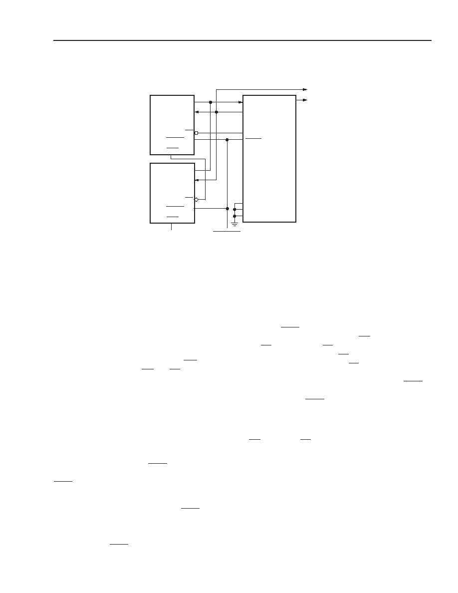
Data Sheet
March, 2003
Lattice Semiconductor
67
ORCA
Series 4 FPGAs
FPGA Configuration Modes
(continued)
Note: M3 = GND for high-speed CCLK; M3 = V
DD
for low-frequency CCLK.
5-4456(F).a
Figure 39. Master Serial Configuration Schematic
DIN
M2
M1
M0
ORCA
SERIES
FPGA
CCLK
DOUT
TO DAISY-
CHAINED
DEVICES
DATA
CLK
CE
CEO
DATA
CLK
RESET/OE
CEO
CE
TO MORE
SERIAL ROMs
AS NEEDED
DONE
PRGM
PROGRAM
RESET/OE
Asynchronous Peripheral Mode
Figure 40 shows the connections needed for the asyn-
chronous peripheral mode. In this mode, the FPGA
system interface is similar to that of a microprocessor-
peripheral interface. The microprocessor generates the
control signals to write an 8-bit byte into the FPGA. The
FPGA control inputs include active-low
CS0
and active-
high CS1 chip selects and
WR
and
RD
inputs. The chip
selects can be cycled or maintained at a static level
during the configuration cycle. Each byte of data is writ-
ten into the FPGA's D[7:0] input pins. D[7:0] of the
FPGA can be connected to D[7:0] of the microproces-
sor only if a standard prom file format is used. If a .bit
or .rbt file is used from ispLEVER, then the user must
mirror the bytes in the .bit or .rbt file OR leave the .bit or
.rbt file unchanged and connect D[7:0] of the FPGA to
D[0:7] of the microprocessor.
The FPGA provides an RDY/
BUSY
status output to indi-
cate that another byte can be loaded. A low on RDY/
BUSY
indicates that the double-buffered hold/shift reg-
isters are not ready to receive data, and this pin must
be monitored to go high before another byte of data
can be written. The shortest time RDY/
BUSY
is low
occurs when a byte is loaded into the hold register and
the shift register is empty, in which case the byte is
immediately transferred to the shift register. The long-
est time for RDY/
BUSY
to remain low occurs when a
byte is loaded into the holding register and the shift
register has just started shifting configuration data into
configuration RAM.
The RDY/
BUSY
status is also available on the D7 pin by
enabling the chip selects, setting
WR
high, and apply-
ing
RD
low, where the
RD
input provides an output
enable for the D[7:3] when
RD
is low. The D[2:0] pins
are not enabled to drive when
RD
is low and, therefore,
only act as input pins in asynchronous peripheral
mode. Optionally, the user can ignore the RDY/
BUSY
status and simply wait until the maximum time it would
take for the RDY/
BUSY
line to go high, indicating the
FPGA is ready for more data, before writing the next
data byte.
The following signals are also available on D[6:3] when
WR
is high and
RD
is low:
D[6:5] is a 2-bit configuration bitstream error descrip-
tion flag: 00= no error, 01 = ID error, 10 = checksum
error, 11 = stop bit/frame alignment error.
D[4:3] is a 2-bit system bus error flag: 00 = no error,
01 = one error occurred, 11 = multiple errors
occurred.
One FPGA in asynchronous peripheral mode can pro-
vide configuration data out on DOUT to additional
FPGAs in a daisy-chain configuration. The configura-
tion data on DOUT is provided synchronously with the
rising edge of CCLK.
68
Lattice Semiconductor
Data Sheet
March, 2003
ORCA
Series 4 FPGAs
FPGA Configuration Modes
(continued)
Note: M3 = GND for high-speed CCLK; M3 = V
DD
for low-frequency CCLK.
5-9739(F).a
Figure 40. Asynchronous Peripheral Configuration
Microprocessor Interface Mode
The built-in MPI in Series 4 FPGAs is designed for use in configuring the FPGA. Figure 41 show the glueless inter-
face for FPGA configuration and readback from the PowerPC processor. When enabled by the mode pins, the MPI
handles all configuration/readback control and handshaking with the host processor. For single FPGA configura-
tion, the host sets the configuration control register MPI_PRGM to one then back to zero and, after reading that the
configuration write data acknowledge register is high, transfers data 8, 16, or 32 bits at a time to the FPGA's D[#:0]
input pins. If configuring multiple FPGAs through daisy-chain operation is desired, the SYS_DAISY bit must be set
in the configuration control register of the MPI.
The configuration control register offers control bits to enable the interrupt on a bit stream error. The
MPI
status
register may be used in conjunction with, or in place of, the interrupt request option. The status register contains a
2-bit field to indicate the bit stream error status. A flow chart of the
MPI
configuration process is shown in Figure 42.
MICRO-
PRGM
ORCA
SERIES
FPGA
DOUT
CCLK
HDC
LDC
M2
M1
M0
V
DD
TO DAISY-
CHAINED
DEVICES
PROCESSOR
D[7:0]
RDY/BUSY
INIT
DONE
ADDRESS
DECODE LOGIC
BUS
CONTROLLER
8
CS0
CS1
RD
WR
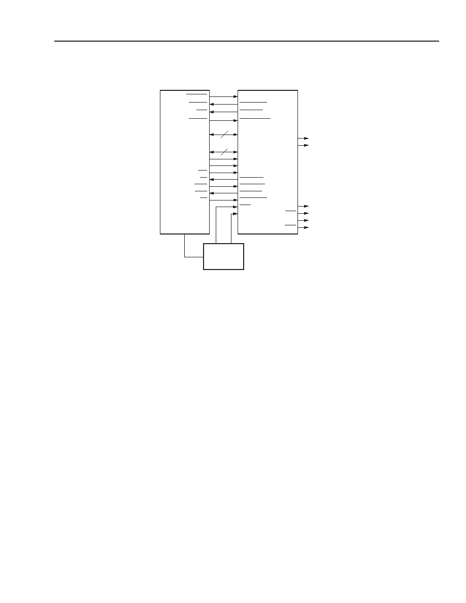
Lattice Semiconductor
69
Data Sheet
March, 2003
ORCA
Series 4 FPGAs
FPGA Configuration Modes
(continued)
5-9738(F).b
Figure 41. PowerPC/MPI Configuration Schematic
Configuration readback can also be performed via the MPI when it is in user mode. The MPI is enabled in user
mode by setting the MP_USER_ENABLE bit to 1 in the configuration control register prior to the start of configura-
tion or through a configuration option. To perform readback, the host processor writes the 14-bit readback start
address to the readback address registers and sets the SYS_RD_CFG bit to one, then back to zero in the configu-
ration control register. Readback data is returned 8 bits at a time to the readback data register and is valid when the
DATA_RDY bit of the status register is 1. There is no error checking during readback. A flow chart of the MPI read-
back operation is shown in Figure 43. The RD_DATA pin used for dedicated FPGA readback is invalid during MPI
readback.
DOUT
CCLK
D[0:n]
PPC_A[14:31]
MPI_CLK
MPI_RW
MPI_ACK
MPI_BDIP
MPI_IRQ
MPI_STRB
CS0
CS1
HDC
LDC
D[0:n]
A[14:31]
CLKOUT
RD/WR
TA
BDIP
IRQx
TS
TO DAISY-
CHAINED
DEVICES
POWERPC
ORCA
8, 16, 32
FPGA
SERIES 4
DONE
INIT
BUS
CONTROLLER
DP[0:m]
DP[0:m]
1, 2, 4
MPI_BURST
BURST
MPI_TEA
TEA
MPI_RTRY
RETRY
MPI_TSZ[0:1]
TSZ[0:1]

70
Lattice Semiconductor
Data Sheet
March, 2003
ORCA
Series 4 FPGAs
FPGA Configuration Modes
(continued)
5-5763(F)
Figure 42. Configuration Through
MPI
POWER ON WITH
WRITE CONFIGURATION
READ STATUS REGISTER
INIT = 1?
NO
READ STATUS REGISTER
BIT STREAM ERROR?
DATA_RDY = 1?
WRITE DATA TO
DONE = 1?
DONE
ERROR
YES
YES
YES
NO
NO
YES
NO
VALID M[3:0]
CONTROL REGISTER BITS
CONFIGURATION DATA REG
WRITE CONFIGURATION
DATA REGISTER

Lattice Semiconductor
71
Data Sheet
March, 2003
ORCA
Series 4 FPGAs
FPGA Configuration Modes
(continued)
5-5764(F)
Figure 43. Readback Through MPI
ENABLE MICROPROCESSOR
SET READBACK ADDRESS
WRITE RD_CFG TO 0
DATA_RDY = 1?
READ DATA REGISTER
START OF FRAME
INCREMENT ADDRESS
DATA = 0xFF?
YES
YES
READ STATUS REGISTER
IN CONTROL REGISTER 1
INTERFACE IN USER MODE
READ DATA REGISTER
FOUND?
READ UNTIL END OF FRAME
FINISHED
READBACK?
COUNTER IN SOFTWARE
YES
YES
WRITE RD_CFG TO 1
IN CONTROL REGISTER 1
STOP
NO
NO
ERROR
NO
ERROR
NO
READ DATA REGISTER
DATA = 0xFF?
YES
NO
ERROR

72
Lattice Semiconductor
Data Sheet
March, 2003
ORCA
Series 4 FPGAs
FPGA Configuration Modes
(continued)
Slave Serial Mode
The slave serial mode is primarily used when multiple FPGAs are configured in a daisy-chain (see the Daisy-
Chaining section). It is also used on the FPGA evaluation board that interfaces to the download cable. A device in
the slave serial mode can be used as the lead device in a daisy-chain. Figure 44 shows the connections for the
slave serial configuration mode.
The configuration data is provided into the FPGA's DIN input synchronous with the configuration clock CCLK input.
After the FPGA has loaded its configuration data, it retransmits the incoming configuration data on DOUT at the ris-
ing edge of CCLK. CCLK is routed into all slave serial mode devices in parallel.
Multiple slave FPGAs can be loaded with identical configurations simultaneously. This is done by loading the con-
figuration data into the DIN inputs in parallel.
5-4485(F).a
Figure 44. Slave Serial Configuration Schematic
Slave Parallel Mode
The slave parallel mode is essentially the same as the slave serial mode except that 8 bits of data are input on pins
D[7:0] for each CCLK cycle. Due to 8 bits of data being input per CCLK cycle, the DOUT pin does not contain a
valid bit stream for slave parallel mode. As a result, the lead device cannot be used in the slave parallel mode in a
daisy-chain configuration.
Figure 45
is a schematic of the connections for the slave parallel configuration mode. WR and CS0 are active-low
chip select signals, and CS1 is an active-high chip select signal. These chip selects allow the user to configure mul-
tiple FPGAs in slave parallel mode using an 8-bit data bus common to all of the FPGAs. These chip selects can
then be used to select the FPGAs to be configured with a given bit stream. The chip selects must be active for each
valid CCLK cycle until the device has been completely programmed. They can be inactive between cycles but must
meet the setup and hold times for each valid positive CCLK. D[7:0] of the FPGA can be connected to D[7:0] of the
microprocessor only if a standard prom file format is used. If a .bit or .rbt file is used from ispLEVER, then the user
must mirror the bytes in the .bit or .rbt file OR leave the .bit or .rbt file unchanged and connect D[7:0] of the FPGA
to D[0:7] of the microprocessor.
MICRO-
PROCESSOR
OR
DOWNLOAD
CABLE
M2
M1
M0
HDC
SERIES
FPGA
LDC
V
DD
CCLK
PRGM
DOUT
TO DAISY-
CHAINED
DEVICES
DONE
DIN
INIT
ORCA
M3

Lattice Semiconductor
73
Data Sheet
March, 2003
ORCA
Series 4 FPGAs
FPGA Configuration Modes
(continued)
5-4487(F).a
Figure 45. Slave Parallel Configuration Schematic
Daisy-Chaining
Multiple FPGAs can be configured by using a daisy-chain of the FPGAs. Daisy-chaining uses a lead FPGA and one
or more FPGAs configured in slave serial mode. The lead FPGA can be configured in any mode except slave paral-
lel mode.
All daisy-chained FPGAs are connected in series. Each FPGA reads and shifts the preamble and length count in on
positive CCLK and out on positive CCLK edges.
An upstream FPGA that has received the preamble and length count outputs a high on DOUT until it has received
the appropriate number of data frames so that downstream FPGAs do not receive frame start indications. After
loading and retransmitting the preamble and length count to a daisy-chain of slave devices, the lead device loads its
configuration data frames. The loading of configuration data continues after the lead device has received its config-
uration data if its internal frame bit counter has not reached the length count. When the configuration RAM is full
and the number of bits received is less than the length count field, the FPGA shifts any additional data out on
DOUT.
The configuration data is read into DIN of slave devices on the positive edge of CCLK, and shifted out DOUT on the
positive edge of CCLK. Figure 46 shows the connections for loading multiple FPGAs in a daisy-chain configuration.
The generation of CCLK for the daisy-chained devices that are in slave serial mode differs depending on the config-
uration mode of the lead device. A master parallel mode device uses its internal timing generator to produce an
internal CCLK at eight times its memory address rate (RCLK). The asynchronous peripheral mode and MPI mode
device outputs eight CCLKs for each write cycle. If the lead device is configured in slave mode, CCLK must be
routed to the lead device and to all of the daisy-chained devices.
MICRO-
PROCESSOR
OR
SYSTEM
D[7:0]
DONE
CCLK
CS1
M2
M1
M0
HDC
LDC
8
V
DD
INIT
PRGM
CS0
WR
SERIES
FPGA
ORCA
M3
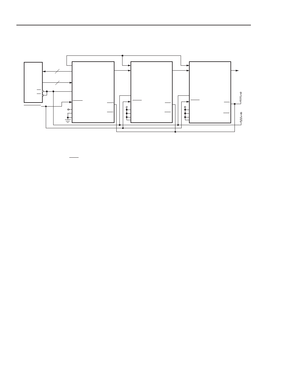
74
Lattice Semiconductor
Data Sheet
March, 2003
ORCA
Series 4 FPGAs
FPGA Configuration Modes
(continued)
5-4488(F).a
Figure 46. Daisy-Chain Configuration Schematic
As seen in Figure 46, the INIT pins for all of the FPGAs are connected together. This is required to guarantee that
powerup and initialization will work correctly. In general, the DONE pins for all of the FPGAs are also connected
together as shown to guarantee that all of the FPGAs enter the start-up state simultaneously. This may not be
required, depending upon the start-up sequence desired.
Daisy-Chaining with Boundary-Scan
Multiple FPGAs can be configured through the JTAG ports by using a daisy-chain of the FPGAs. This daisy-chain-
ing operation is available upon initial configuration after powerup, after a power-on reset, after pulling the program
pin to reset the chip, or during a reconfiguration if the EN_JTAG RAM has been set.
All daisy-chained FPGAs are connected in series. Each FPGA reads and shifts the preamble and length count in
on the positive TCK and out on the negative TCK edges.
An upstream FPGA that has received the preamble and length count outputs a high on TDO until it has received
the appropriate number of data frames so that downstream FPGAs do not receive frame start bit pairs. After load-
ing and retransmitting the preamble and length count to a daisy-chain of downstream devices, the lead device
loads its configuration data frames.
The loading of configuration data continues after the lead device had received its configuration read into TDI of
downstream devices on the positive edge of TCK, and shifted out TDO on the negative edge of TCK.
V
DD
EPROM
PROGRAM
OE
CE
M2
M1
M0
DONE
HDC
LDC
RCLK
CCLK
DOUT
DIN
DOUT
DIN
CCLK
DONE
DOUT
INIT
INIT
INIT
CCLK
V
DD
PRGM
PRGM
PRGM
HDC
LDC
RCLK
HDC
LDC
RCLK
V
DD
ORCA
SERIES
FPGA
SLAVE 2
ORCA
SERIES
FPGA
MASTER
ORCA
SERIES
FPGA
SLAVE 1
A[17:0]
A[17:0]
D[7:0]
D[7:0]
DONE
M3
M2
M1
M0
V
DD
M3
M2
M1
M0
V
DD
Lattice Semiconductor
75
Data Sheet
March, 2003
ORCA
Series 4 FPGAs
Absolute Maximum Ratings
Stresses in excess of the absolute maximum ratings can cause permanent damage to the device. These are abso-
lute stress ratings only. Functional operation of the device is not implied at these or any other conditions in excess
of those given in the operations sections of this data sheet. Exposure to absolute maximum ratings for extended
periods can adversely affect device reliability.
The ORCA Series FPGAs include circuitry designed to protect the chips from damaging substrate injection currents
and to prevent accumulations of static charge. Nevertheless, conventional precautions should be observed during
storage, handling, and use to avoid exposure to excessive electrical stress.
Table 34. Absolute Maximum Ratings
Recommended Operating Conditions
Table 35. Recommended Operating Conditions
Note:
1. The maximum recommended junction temperature (T
J
) during operation is 125 �C.
2. Timing parameters in this data sheet an ispLEVER are characterized under higher voltage and temperature conditions than the recom-
mended operating conditions in this table.
3. The internal PLLs operate from the V
DD
33 power supply. This power supply should be well isolated from all other power supplies on the board
for proper operation.
Parameter
Symbol
Min
Max
Unit
Storage Temperature
T
stg
�65
150
�C
Power Supply Voltage with Respect to Ground
V
DD
33
�0.3
4.2
V
V
DD
IO
�0.3
4.2
V
V
DD
15
�0.3
2.0
V
Input Signal with Respect to Ground
V
IN
� 0.3
V
DD
IO + 0.3
V
Signal Applied to High-impedance Output
--
� 0.3
V
DD
IO + 0.3
V
Maximum Package Body (Soldering) Temperature
--
--
220
�C
Parameter
Symbol
Min
Max
Unit
Power Supply Voltage with Respect to Ground
V
DD
33
3.0
3.6
V
V
DD
IO
1.4
3.6
V
V
DD
15
1.425
1.575
V
Input Signal with Respect to Ground
V
IN
� 0.3
V
DD
IO + 0.3
V
Junction Temperature
T
J
�40
125
�C

76
Lattice Semiconductor
Data Sheet
March, 2003
ORCA
Series 4 FPGAs
Electrical Characteristics
Table 36. Electrical Characteristics
OR4Exx Industrial: V
DD
15 = 1.4 V to 1.6 V, V
DD
33 = 3.0 V to 3.6 V, V
DD
IO = 3.0 V to 3.6 V, �40 �C
<
T
A
<
+125
�C;
C
L
=
30 pF.
* The pull-up resistor will externally pull the pin to a level 1.0 V below V
DD
IO.
Note: 1. The Standby Current for V
DD
IO is variable depending upon I/O types. For LVTTL I/O held at V
DD
IO or GND, this value is typically less
than 1 mA.
Parameter
Symbol
Test Conditions
OR4Exx
Unit
Min
Typ
Max
Input Leakage Current
I
L
V
DD
IO = max, V
IN
= V
SS
or
V
DD
IO
� 10
--
10
�A
Standby Current (V
DD
15
):
OR4E02
OR4E04
OR4E06
I
DD
SB15
T
A
= 25 �C, V
DD
15
=
1.6 V,
V
DD
33
= 3.6 V, V
DD
IO = 3.6 V,
internal oscillator running, no output loads,
inputs V
DD
IO or V
SS
(after configuration)
--
--
--
5
10
15
200
200
200
mA
mA
mA
Same conditions except T
A
= 85 �C
--
--
500
mA
Standby Current (V
DD
33
)
:
OR4E02
OR4E04
OR4E06
I
DD
SB33
T
A
= 25 �C, V
DD
15
=
1.6 V,
V
DD
33
= 3.6 V, V
DD
IO = 3.6 V,
internal oscillator stopped, no output loads,
inputs V
DD
IO or GND (after configuration)
--
--
--
4
7
10
100
100
100
mA
mA
mA
Same conditions except T
A
= 85 �C
--
--
300
mA
Data Retention Voltage
(V
DD
33
)
V
DR
33
T
J
= �40 �C to 125 �C
2.3
--
--
V
Data Retention Voltage
(V
DD
15
)
V
DR
15
T
J
= �40 �C to 125 �C
1.1
--
--
V
DC Input Levels
V
IL
V
IH
Input levels vary per input standard. See the
Series 4 IO Application Note for details
Various
--
Various
V
DC Output Levels
V
OL
V
OH
Output levels vary per output standard. See
the Series 4 IO Application Note for details
Various
--
Various
V
Output Drive Currents
I
OL
I
OH
Output currents vary per output standard.
See the Series 4 IO Application Note for
details
Various
--
Various
mA
Input Capacitance
C
IN
T
A
= 25 �C, V
DD
IO = 3.6 V,
Test frequency = 1 MHz
--
--
5
pF
Output Capacitance
C
OUT
T
A
= 25 �C, V
DD
IO = 3.6 V,
Test frequency = 1 MHz
--
--
5
pF
DONE Pull-up
Resistor*
R
DONE
V
DD
IO = 3.0 V to 3.6 V, V
IN
= V
SS
,
T
J
= �40 �C to 125 �C
100
--
--
k
M[3:0] Pull-up
Resistors*
R
M
V
DD
IO = 3.0 V to 3.6 V, V
IN
= V
SS
,
T
J
= �40 �C to 125 �C
100
--
--
k
I/O Pad Static Pull-up
Current*
I
PU
V
DD
IO = 3.0 V to 3.6 V, V
IN
= V
SS
,
T
J
= �40 �C to 125 �C
14.4
--
50.9
�A
I/O Pad Static
Pull-down Current
I
PD
V
DD
IO = 3.0 V to 3.6 V, V
IN
= V
SS
,
T
J
= �40 �C to 125 �C
26
--
103
�A
I/O Pad Pull-up
Resistor*
R
PU
V
DD
IO = 3.0 V to 3.6 V, V
IN
= V
SS
,
T
J
= �40 �C to 125 �C
100
--
--
k
I/O Pad Pull-down
Resistor
R
PD
V
DD
IO = 3.0 V to 3.6 V, V
IN
= V
DD
,
T
J
= �40 �C to 125 �C
50
--
--
k

Lattice Semiconductor
77
Data Sheet
March, 2003
ORCA
Series 4 FPGAs
Power Estimation
A spreadsheet is available in ispLEVER for detailed
power estimates based on circuit implementation
details from ispLEVER and user inputs. A quick esti-
mate of power dissipation for a Series 4 device is now
presented.
Estimating Power Dissipation
The total operating power dissipated is estimated by
adding the standby (I
DD
SB), internal, and external
power dissipated. The internal and external power is
the power consumed in the PLCs and PICs, respec-
tively. In general, the standby power is small and may
be neglected. The total operating power is as follows:
P
T
=
P
INT
+
P
IO
+ P
CLK
The internal operating power is made up of two parts:
clock generation and PFU/EBR/PIO power. The PFU/
EBR/PIO power can be estimated per output based
upon the number of PFU/EBR/PIO outputs switching
when driving a typical fanout (three X6 lines and nine
X1 lines).
P
INT
= 0.015 mW/MHz
For each PFU/EBR/PIO output that switches, 0.015
mW/MHz needs to be multiplied times the frequency (in
MHz) that the output switches. Generally, this can be
estimated by using the clock rate multiplied by some
activity factor; for example, 20%.
The power dissipated by clocks is due to either global
primary clock networks or secondary/edge clock net-
works. Their power has a fixed component and a vari-
able component based on the number of PFUs, PIOs,
or EBRs that use that clock as follows:
Primary: 0.143 mW/MHz + (0.0033mW/MHz x num-
ber of blocks driven)
Secondary: 0.06 mW/MHz + (0.0029mW/MHz x
number of blocks driven)
Clock power is calculated from these equations by mul-
tiplying times the clock frequency in MHz. Note that an
activity factor (i.e., 100% activity) is not used to calcu-
late clock power.
The device I/O power dissipated is the sum of the
power dissipated in the four PIOs in the PIC. This con-
sists of power dissipated by inputs and ac power dissi-
pated by outputs. The power dissipated in each PIO
depends on whether it is configured as an input, out-
put, or input/output. If a PIO is operating as an output,
then there is a power dissipation component for P
IN
, as
well as P
OUT
. This is because the output feeds back to
the input.
The power dissipated by a LVCMOS2 input buffer is
(V
IH
= V
DD
� 0.3 V or higher) estimated as:
P
IN
= 0.09 mW/MHz
The ac power dissipation from a LVCMOS2 output or
bidirectional is estimated by the following:
P
OUT
= (C
L
+ 5.0 pF) x V
DD
2
x F Watts
where the unit for C
L
(the output capacitive load) is Far-
ads, and the unit for F is Hz.
For all other I/O buffer types other than LVCMOS2, see
the detailed power estimation spreadsheet available in
ispLEVER.

78
Lattice Semiconductor
Data Sheet
March, 2003
ORCA
Series 4 FPGAs
Timing Characteristics
To define speed grades, the ORCA series part number designation (see Ordering Information) uses a single-digit
number to designate a speed grade. This number is not related to any single ac parameter. Higher numbers indi-
cate a faster set of timing parameters. The actual speed sorting is based on testing the delay in a path consisting of
an input buffer, combinatorial delay through all PLCs in a row, and an output buffer. Other tests are then done to
verify other delay parameters, such as routing delays, setup times to FFs, etc.
The most accurate timing characteristics are reported by the timing analyzer in ispLEVERTM design software. A
timing report provided by the development system after layout divides path delays into logic and routing delays.
The timing analyzer can also provide logic delays prior to layout. While this allows routing budget estimates, there
is wide variance in routing delays associated with different layouts.
The logic timing parameters noted in the Electrical Characteristics section of this data sheet are the same as those
in ispLEVER. In the timing tables that follow, symbol names are generally a concatenation of the PFU operating
mode (as defined in Table 3) and the parameter type. The setup, hold, and propagation delay parameters, defined
below, are designated in the symbol name by the SET, HLD, and DEL characters, respectively. The values given
for the parameters are the same as those used during production testing and speed binning of the devices. The
junction temperature and supply voltage used to characterize the devices are listed in the delay tables and the
delay values in this data sheet are from ispLEVER. Actual delays at nominal temperature and voltage for best-case
processes can be much better than the values given.
It should be noted that the junction temperature used in the tables is generally 85 �C or 100 �C, based on the tem-
perature grade of the device. The junction temperature for the FPGA depends on the power dissipated by the
device, the package thermal characteristics (
JA
), and the ambient temperature, as calculated in the following
equation and as discussed further in the Package Thermal Characteristics section:
T
Jmax =
T
Amax
+ (P �
JA
) �C
Note: The user must determine this junction temperature to see if the delays from ispLEVER should be derated
based on the following derating tables.
Table 37--Table 38 provide approximate power supply and junction temperature derating for Series 4 commercial
and industrial devices. The delay values in this data sheet and reported by ispLEVER are shown as 1.00 in the
tables. The method for determining the maximum junction temperature is defined in the Package Thermal Charac-
teristics section. Taken cumulatively, the range of parameter values for best-case vs. worst-case processing, sup-
ply voltage, and junction temperature can approach 3 to 1.
The typical timing path in Series 4 is made up of both 3.3 V (V
DD
IO and/or V
DD
33) components and 1.5 V (V
DD
15)
components. For example, all I/O circuits use V
DD
IO at the device interface but all internal routing and I/O register
logic use V
DD
15. Thus actual voltage derating needs to be done based on multiple parameters. A simple approxi-
mation is that 50% of the delay path is due to each of these parameters. All internal paths use V
DD
15 for logic and
V
DD
33 for routing, but if V
DD
33 remains above 3.0 V the internal delays can be assumed to be dependent on
V
DD
15 derating values only. Note however that temperature derating is approximately the same percentage for all
three supply voltages thus allowing one temperature derating value to be used. For the most accurate results, volt-
age and temperature derating capabilities to be released in ispLEVER should be used.
Lattice Semiconductor
79
Data Sheet
March, 2003
ORCA
Series 4 FPGAs
Timing Characteristics
(continued)
Table 37. I/O Derating for 3.3 V I/Os (V
DD
IO)--Only valid for TTL/CMOS I/Os
Table 38. Internal Derating for 1.5V (V
DD
15)
In addition to supply voltage, process variation, and operating temperature, circuit and process improvements of
the ORCA Series FPGAs over time will result in significant improvement of the actual performance over those listed
for a speed grade. Even though lower speed grades may still be available, the distribution of yield to timing param-
eters may be several speed grades higher than that designated on a product brand. Design practices need to con-
sider best-case timing parameters (e.g., delays = 0), as well as worst-case timing.
The routing delays are a function of fan-out and the capacitance associated with the CIPs and metal interconnect in
the path. The number of logic elements that can be driven (fan-out) by PFUs is unlimited, although the delay to
reach a valid logic level can exceed timing requirements. It is difficult to make accurate routing delay estimates prior
to design compilation based on fan-out. This is because the CAE software may delete redundant logic inserted by
the designer to reduce fan-out, and/or it may also automatically reduce fan-out by net splitting.
The waveform test points are given in the Input/Output Buffer Measurement Conditions section of this data sheet.
The timing parameters given in the electrical characteristics tables in this data sheet follow industry practices, and
the values they reflect are described below.
T
J
(�C)
Commercial
T
J
(�C)
Industrial
Power Supply Voltage
3.0 V
3.15 V
3.3 V
3.45 V
3.6 V
�
�40
0.82
0.80
0.77
0.75
0.74
�40
�25
0.83
0.81
0.78
0.76
0.75
0
15
0.87
0.84
0.81
0.80
0.78
25
40
0.91
0.88
0.85
0.82
0.81
85
100
1.00
0.97
0.93
0.91
0.88
100
115
1.02
0.99
0.96
0.93
0.90
110
125
1.05
1.01
0.97
0.95
0.92
125
�
1.07
1.03
0.99
0.97
0.94
T
J
(�C)
Commercial
T
J
(�C)
Industrial
Power Supply Voltage
1.40 V
1.425 V
1.500 V
1.575 V
1.6 V
�
�40
0.87
0.85
0.82
0.79
0.78
�40
�25
0.89
0.87
0.83
0.80
0.79
0
15
0.93
0.91
0.87
0.82
0.81
25
40
0.96
0.94
0.89
0.85
0.84
85
100
1.02
1.00
0.95
0.91
0.90
100
115
1.04
1.02
0.97
0.93
0.92
110
125
1.05
1.03
0.98
0.94
0.93
125
�
1.06
1.05
1.00
0.96
0.95
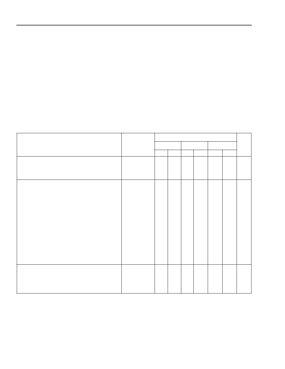
80
Lattice Semiconductor
Data Sheet
March, 2003
ORCA
Series 4 FPGAs
Timing Characteristics
(continued)
Propagation Delay--The time between the specified reference points. The delays provided are the worst case of
the tphh and tpll delays for noninverting functions, tplh and tphl for inverting functions, and tphz and tplz for 3-state
enable.
Setup Time--The interval immediately preceding the transition of a clock or latch enable signal, during which the
data must be stable to ensure it is recognized as the intended value.
Hold Time--The interval immediately following the transition of a clock or latch enable signal, during which the
data must be held stable to ensure it is recognized as the intended value.
3-State Enable--The time from when a 3-state control signal becomes active and the output pad reaches the
high-impedance state.
Table 39. PFU Timing Parameters
OR4Exx commercial: VDD15 = 1.425 V, VDD33 = 3.0 V, TJ = +85 �C
OR4Exx industrial: VDD15 = 1.425 V, VDD33 = 3.0 V, TJ = +100 �C
Note:
A complete listing of PFU Timing Parameters can be displayed in ispLEVER. This is a sampling of the key timing parameters.
Parameter
Symbol
Speed
Unit
�1
�2
�3
Min Max Min Max
Min
Max
Combinatorial Delays:
Four-input Variables to LUT out
Five-input Variables to LUT out
Six-input Variables to LUT out
F4_DEL
F5_DEL
F6_DEL
--
--
--
0.66
0.77
1.10
--
--
--
0.55
0.64
0.81
--
--
--
0.50
0.58
0.74
ns
ns
ns
Sequential Delays:
CLK Low Time
CLK High Time
Four-input Variables to Register CLK setup
Five-input Variables to Register CLK setup
Six-input Variables to Register CLK setup
Data In to Register CLK setup
Four-input Variables from Register CLK hold
Five-input Variables from Register CLK hold
Six-input Variables from Register CLK hold
Data In from Register CLK hold
Register CLK to Out
CLKL_MPW
CLKH_MPW
F4_SET
F5_SET
F6_SET
DIN_SET
F4_HLD
F5_HLD
F6_HLD
DIN-HLD
REG_DEL
0.36
0.40
0.28
0.38
0.71
0.00
0.00
0.10
0.00
0.25
1.03
--
--
--
--
--
--
--
--
--
--
--
0.35
0.38
0.23
0.28
0.63
0.00
0.00
0.16
0.10
0.24
0.92
--
--
--
--
--
--
--
--
--
--
--
0.32
0.35
0.21
0.25
0.57
0.00
0.00
0.15
0.09
0.22
0.84
--
--
--
--
--
--
--
--
--
--
--
ns
ns
ns
ns
ns
ns
ns
ns
ns
ns
ns
PFU CLK to Out (REG_DEL) Delay Adjustments
from Cycle Stealing:
One Delay Cell
Two Delay Cells
Three Delay Cells
CYCDEL1
CYCDEL2
CYCDEL3
0.89
1.64
2.43
--
--
--
0.70
1.29
1.98
--
--
--
0.64
1.18
1.80
--
--
--
ns
ns
ns
Lattice Semiconductor
81
Data Sheet
March, 2003
ORCA
Series 4 FPGAs
Timing Characteristics
(continued)
Table 40. PFU used as Dual-Port RAM: Sync. Write and Sync. or Async. Read Timing Characteristics
OR4Exx commercial: VDD15 = 1.425 V, VDD33 = 3.0 V, TJ = +85 �C
OR4Exx industrial: VDD15 = 1.425 V, VDD33 = 3.0 V, TJ = +100 �C
Note: A complete listing of PFU timing parameters can be displayed in ispLEVER. This is a sampling of the key timing parameters.
Parameter
Symbol
Speed
Unit
-1
-2
-3
Min
Max
Min
Max
Min
Max
Write Operation for RAM Mode:
Maximum Write Clock Frequency
Write Data to CLK Setup Time
Write CLK to Data Out
SMWCLK_FRQ
WD_SET
MEM_DEL
--
0.32
--
300.00
--
2.21
--
0.24
--
382.00
--
1.89
--
0.22
--
422.00
--
1.71
MHz
ns
ns
Async Read Operation for RAM Mode:
Data Out Valid After Address
RA_DEL
--
0.66
--
0.55
--
0.50
ns
Sync Read Operation for RAM Mode:
Maximum Read Clock Frequency
Read CLK to Data Out
SMRCLK_FRQ
REG_DEL
--
--
300.00
1.03
--
--
382.00
0.92
--
--
422.00
0.84
MHz
ns
82
Lattice Semiconductor
Data Sheet
March, 2003
ORCA
Series 4 FPGAs
Timing Characteristics
(continued)
Table 41. Embedded Block RAM (EBR) Timing Characteristics (512 x 18) Quad-Port RAM Mode
OR4Exx commercial: VDD15 = 1.425 V, VDD33 = 3.0 V, TJ = +85 �C
OR4Exx industrial: VDD15 = 1.425 V, VDD33 = 3.0 V, TJ = +100 �C
Note: A complete listing of EBR Timing Parameters can be displayed in ispLEVER. This is a sampling of the key timing parameters.
Table 42. Supplemental Logic and Interconnect Cell (SLIC) Timing Characteristics
OR4Exx commercial: VDD15 = 1.425 V, VDD33 = 3.0 V, TJ = +85 �C
OR4Exx industrial: VDD15 = 1.425 V, VDD33 = 3.0 V, TJ = +100 �C
Note: A complete listing of SLIC Timing Parameters can be displayed in ispLEVER. This is a sampling of the key timing parameters.
Parameter
Symbol
Speed
Unit
-1
-2
-3
Min
Max
Min
Max
Min
Max
Write Operation for RAM Mode:
Maximum Write Clock Frequency
Write Data to Write Clock Setup Time
Write Address to Write Clock Setup Time
EBRWCLK_FRQ
D*_CKW*_SET
A*_CKW*_SET
--
0.28
0.40
200.0
--
--
--
0.31
0.38
217.0
--
--
--
0.28
0.35
225.0
--
--
MHz
ns
ns
Async Read Operation for RAM Mode:
Data Out Valid After Read Address
EBR_RA_DEL
--
6.38
--
6.00
--
5.46
ns
Sync Read Operation for RAM Mode:
Maximum Read Clock Frequency
Read Address to Read Clock Setup Time
(OUTREG Mode)
Read Clock to Data Out (IOREG or OUT-
REG modes)
EBRRCLK_FRQ
AR*_CKR*_SET
CKR*_Q*_DEL
--
--
--
200.0
3.61
3.05
--
--
--
217.0
3.45
2.84
--
--
--
225.0
3.13
2.59
MHz
ns
ns
Parameter
Symbol
Speed
Unit
-1
-2
-3
Min
Max
Min Max Min Max
3-Statable BIDIs
BIDI Buffer Delay
BIDI 3-state Enable/Disable Delay
BUF_DEL
TRI_DEL
--
--
0.35
0.39
--
--
0.35
0.35
--
--
0.32
0.32
ns
ns
Decoder
Decoder Delay (BR[9:8], BL[9:8] to DEC)
DEC_DEL
--
0.89
--
0.81
--
0.73
--

Lattice Semiconductor
83
Data Sheet
March, 2003
ORCA
Series 4 FPGAs
Timing Characteristics
(continued)
Table 43. PIO Input Buffer Timing Characteristics
OR4Exx commercial: VDD15 = 1.425 V, VDD33 = 3.0 V, VDDIO = Min, TJ = +85 �C
OR4Exx industrial: VDD15 = 1.425 V, VDD33 = 3.0 V, VDDIO = Min, TJ = +100 �C
Notes:
The delays for all input buffers assume an input rise/fall time of <1 V/ns.
The values in the above table should be used to modify the information in Table 46 through Table 52, which are all based on LVTTL input timing.
Parameter
Symbol
Speed
Unit
-1
-2
-3
Min
Max
Min
Max
Min
Max
Input Delays
Input Rise Time
IN_RIS
--
100
--
100
--
100
ns
Input Fall Time
IN_FAL
--
100
--
100
--
100
ns
Input Delay Adjustments from LVTTL:
LVCMOS2 (2.5 V)
LVCMOS18 (1.8 V)
LVDS
LVPECL
PCI_33 (3.3 V)
PCI_66 (3.3 V)
GTL
GTLP (GTL+)
HSTL_I
HSTL_II
HSTL_III
HSTL_IV
SSTL2_I
SSTL2_II
SSTL3_I
SSTL3_II
PECL
IN_LVCMOS25
IN_LVCMOS15
IN_LVDS
IN_LVPECL
IN_PCI_33
IN_PCI_66
IN_GTL
IN_GTLP
IN_HSTL_I
IN_HSTL_II
IN_HSTL_III
IN_HSTL_IV
IN_SSTL2_I
IN_SSTL2_II
IN_SSTL3_I
IN_SSTL3_II
IN_PECL
--
--
--
--
--
--
--
--
--
--
--
--
--
--
--
--
--
0.54
1.91
�0.04
�0.31
0.59
0.59
5.32
1.87
�0.05
�0.05
�0.20
�0.20
2.28
2.28
0.78
0.78
0.83
--
--
--
--
--
--
--
--
--
--
--
--
--
--
--
--
--
0.44
1.50
0.10
�0.21
0.50
0.50
4.68
2.04
�0.06
�0.06
�0.13
�0.13
1.66
1.66
0.69
0.69
0.72
--
--
--
--
--
--
--
--
--
--
--
--
--
--
--
--
--
0.40
1.36
0.09
�0.19
0.45
0.45
4.26
1.86
�0.06
�0.06
�0.12
�0.12
1.51
1.51
0.63
0.63
0.65
ns
ns
ns
ns
ns
ns
ns
ns
ns
ns
ns
ns
ns
ns
ns
ns
ns
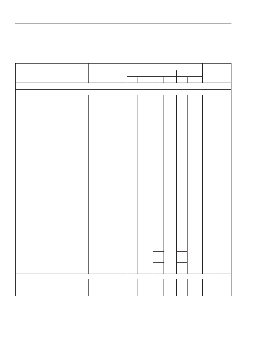
84
Lattice Semiconductor
Data Sheet
March, 2003
ORCA
Series 4 FPGAs
Timing Characteristics
(continued)
Table 44. PIO Output Buffer Timing Characteristics
OR4Exx commercial: VDD15 = 1.425 V, VDD33 = 3.0 V, VDDIO = Min, TJ = +85 �C
OR4Exx industrial: VDD15 = 1.425 V, VDD33 = 3.0 V, VDDIO = Min, TJ = +100 �C
* See the Series 4 PIO Application note for output load conditions on these output buffer types.
Note: The values in the above table should be used to modify the information in Table 46 through Table 48, which are all based on OLVTTL_F12
outputs.
Parameter
Symbol
Speed
Unit
Output
Load
(pF)
-1
-2
-3
Min
Max
Min Max Min
Max
Output Delays
Output Delay Adjustments from OLVTTL_F12:
LVTTL_S6 (Slew Limited, 6 mA)
OUT_LVTTL_S6
--
2.01
--
1.72
--
1.56
ns
30 pF
LVTTL_S12 (Slew Limited, 12 mA)
OUT_LVTTL_S12
--
1.25
--
1.06
--
0.97
ns
30 pF
LVTTL_S24 (Slew Limited, 24 mA)
OUT_LVTTL_S24
--
0.76
--
0.60
--
0.55
ns
30 pF
LVTTL_F6 (Fast, 6 mA)
OUT_LVTTL_F6
--
0.72
--
0.68
--
0.61
ns
30 pF
LVTTL_F24 (Fast, 24 mA)
OUT_LVTTL_F24
--
�0.35
--
�0.32
--
�0.29
ns
30 pF
LVCMOS18_S6 (Slew Limited, 6 mA)
OUT_CMOS18_S6
--
6.91
--
5.36
--
4.87
ns
30 pF
LVCMOS18_S12 (Slew Limited, 12 mA)
OUT_CMOS18_S12
--
6.23
--
3.90
--
3.55
ns
30 pF
LVCMOS18_S24 (Slew Limited, 24 mA)
OUT_CMOS18_S24
--
4.50
--
3.29
--
2.99
ns
30 pF
LVCMOS18_F6 (Fast, 6 mA)
OUT_CMOS18_F6
--
4.75
--
3.83
--
3.48
ns
30 pF
LVCMOS18_F12 (Fast, 12 mA)
OUT_CMOS18_F12
--
2.38
--
1.86
--
1.69
ns
30 pF
LVCMOS18_F24 (Fast, 24 mA)
OUT_CMOS18_F24
--
1.23
--
0.90
--
0.82
ns
30 pF
LVCMOS2_S6 (Slew Limited, 6 mA)
OUT_CMOS18_S6
--
3.26
--
2.66
--
2.42
ns
30 pF
LVCMOS2_S12 (Slew Limited, 12 mA)
OUT_CMOS18_S12
--
2.09
--
1.69
--
1.54
ns
30 pF
LVCMOS2_S24(Slew Limited, 24 mA)
OUT_CMOS18_S24
--
1.58
--
1.23
--
1.12
ns
30 pF
LVCMOS2_F6 (Fast, 6 mA)
OUT_CMOS18_F6
--
1.80
--
1.59
--
1.44
ns
30 pF
LVCMOS2_F12 (Fast, 12 mA)
OUT_CMOS18_F12
--
0.61
--
0.50
--
0.45
ns
30 pF
LVCMOS2_F24 (Fast, 24 mA)
OUT_CMOS18_F24
--
0.03
--
�0.03
--
�0.03
ns
30 pF
LVDS
OUT_LVDS
--
0.07
--
0.00
--
0.00
ns
*
LVPECL
OUT_LVPECL
--
�0.57
--
�0.55
--
�0.50
ns
*
PCI_33 (3.3V)
OUT_PCI_33
--
4.84
--
3.42
--
3.11
ns
10 pF
PCI_66 (3.3V)
OUT_PCI_66
--
4.84
--
3.42
--
3.11
ns
10 pF
GTL
OUT_GTL
--
3.22
--
2.45
--
2.23
ns
*
GTLP (GTL+)
OUT_GTLP
--
3.60
--
2.76
--
2.51
ns
*
HSTL_I
OUT_HSTL_I
--
1.89
--
1.30
--
1.18
ns
20 pF
HSTL_II
OUT_HSTL_II
--
1.89
--
1.30
--
1.18
ns
20 pF
HSTL_III
OUT_HSTL_III
--
2.78
--
1.78
--
1.62
ns
20 pF
HSTL_IV
OUT_HSTL_IV
--
2.78
--
1.78
--
1.62
ns
20 pF
SSTL2_I
OUT_SSTL2_I
--
�0.15
--
�0.18
--
�0.16
ns
30 pF
SSTL2_II
OUT_SSTL2_II
--
�0.15
--
�0.18
--
�0.16
ns
30 pF
SSTL3_I
OUT_SSTL3_I
--
�0.50
--
�0.41
--
�0.37
ns
30 pF
SSTL3_II
OUT_SSTL3_II
--
�0.50
--
�0.41
--
�0.37
ns
30 pF
PECL
OUT_PECL
--
0.12
--
0.16
--
0.15
ns
25 pF
Output Delay Adjustments from Cycle Stealing (typically used to adjust setup vs. clk->out):
One Delay Cell
OCYCDEL1
0.89
--
0.70
--
0.64
--
ns
--
Two Delay Cells
OCYCDEL2
1.64
--
1.29
--
1.18
--
ns
--
Three Delay Cells
OCYCDEL3
2.43
--
1.98
--
1.80
--
ns
--

Lattice Semiconductor
85
Data Sheet
March, 2003
ORCA
Series 4 FPGAs
Timing Characteristics
(continued)
Table 45. Primary Clock Skew to any PFU or PIO Register
OR4Exx commercial/industrial: VDD15 = 1.425 V to 1.575 V, VDD33 = 3.0 V to 3.6 V, �40 �C
<
TJ
<
+125 �C
.
Table 46. Secondary Clock to Output Delay without on-chip PLLs (Pin-to-Pin)
OR4Exx commercial: VDD15 = 1.425 V to 1.575 V, VDD33 = 3.0 V to 3.6 V, VDDIO = 3.0 V to 3.6 V, �40 �C
<
TJ
<
+85 �C.;
CL = 30 pF
OR4Exx industrial: VDD15 = 1.425 V to 1.575 V, VDD33 = 3.0 V to 3.6 V, VDDIO = 3.0 V to 3.6 V, �40 �C
<
TJ
<
+100 �C.;
CL = 30 pF.
Notes:
1. Timing is without the use of the phase-locked loops (PLLs).
2. This clock delay is for a fully routed clock tree that uses the secondary clock network. It includes the LVTTL (3.3 V) input clock buffer, the clock
routing to the PIO CLK input, the clockQ of the FF, and the delay through the LVTTL (3.3 V) data output buffer. An SCLK input clock can be
at any input pin.
3. For timing improvements using other I/O buffer types for the input clock buffer or output data buffer, see Table 53 and Table 55.
5-4846(F).a
Figure 47. Secondary CLK to Output Delay
Description
Device
Speed
Unit
-1
-2
-3
Min
Max
Min
Max
Min
Max
Primary Clock Skew Information (pos edge to
pos edge or neg edge to neg edge)
OR4E02
OR4E04
OR4E06
--
--
--
85
110
120
--
--
--
75
95
105
--
--
--
70
90
100
ps
ps
ps
Primary Clock Skew Information (pos edge to
pos edge, neg edge to neg edge, pos edge to
neg edge or neg edge to pos edge)
OR4E02
OR4E04
OR4E06
--
--
--
265
285
300
--
--
--
190
210
220
--
--
--
180
200
210
ps
ps
ps
Description
Device
Speed
Unit
-1
-2
-3
Min
Max
Min
Max
Min
Max
SCLK OUTPUT Pin (LVTTL-12 mA Fast,
Output within 6 PICs of SCLK input)
All
--
7.22
--
6.70
--
6.06
ns
Additional Delay per each extra 6 PICs per
clock route direction.
All
--
0.36
--
0.38
--
0.34
ns
OUTPUT (30 pF LOAD)
Q
D
SCLK
PIO FF
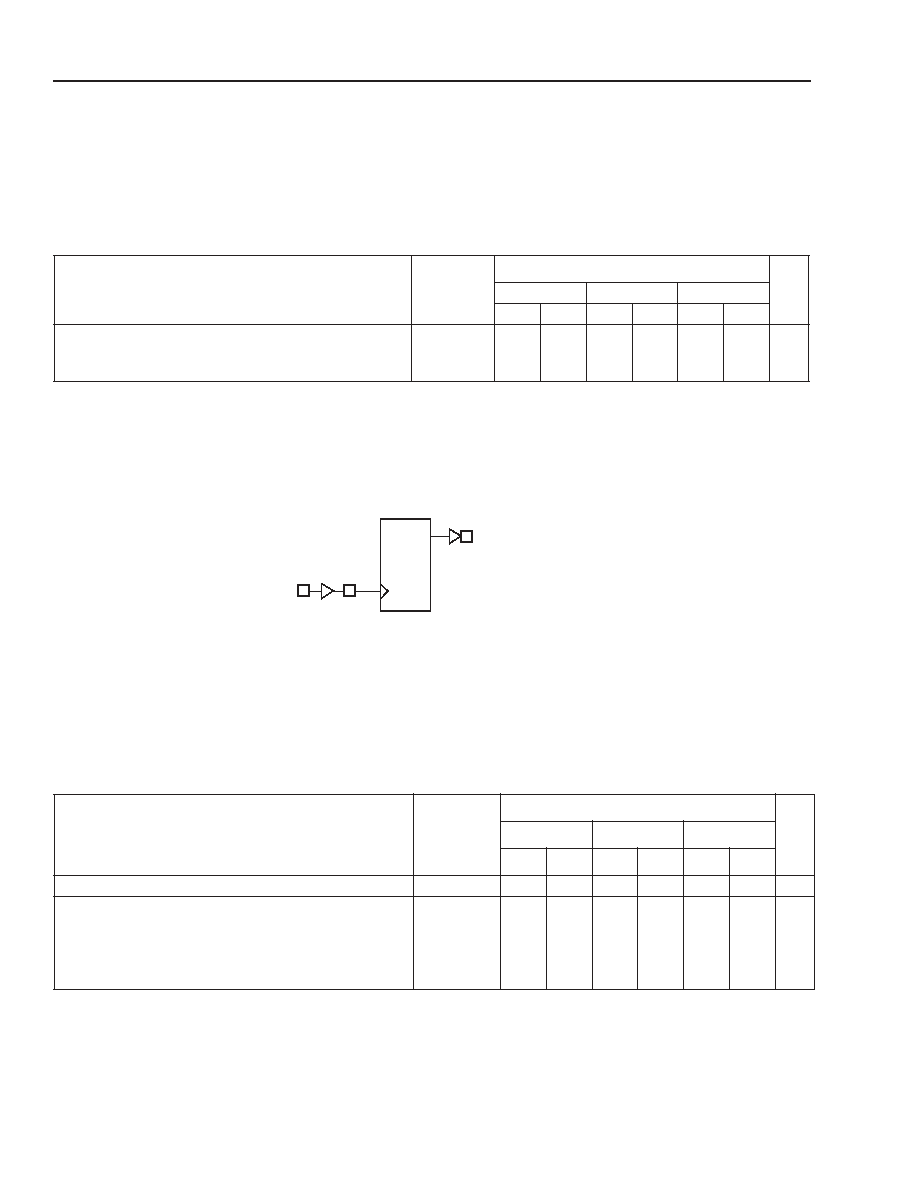
86
Lattice Semiconductor
Data Sheet
March, 2003
ORCA
Series 4 FPGAs
Timing Characteristics
(continued)
Table 47. Primary CLK (PCLK) to Output Delay without on-chip PLLs (Pin-to-Pin)
OR4Exx commercial: VDD15 = 1.425 V to 1.575 V, VDD33 = 3.0 V to 3.6 V, VDDIO = 3.0 V to 3.6 V, �40 �C
<
TJ
<
+85 �C;
CL = 30 p.
OR4Exx industrial: VDD15 = 1.425 V to 1.575 V, VDD33 = 3.0 V to 3.6 V, VDDIO = 3.0 V to 3.6 V, �40 �C
<
TJ
<
+100 �C;
CL = 30 p.
Notes:
1. Timing is without the use of the phase-locked loops (PLLs).
2. This clock delay is for a fully routed clock tree that uses the primary clock network. It includes both the LVTTL (3.3 V) input clock buffer delay,
the clock routing to the PIO CLK input, the clockQ of the FF, and the delay through the LVTTL (3.3 V) data output buffer. The PCLK input
clock is connected at the semi-dedicated primary clock input pins.
3. For timing improvements using other I/O buffer types for the input clock buffer or output data buffer, see Table 53 and Table 55.
5-4846(F).b
Figure 48. Primary Clock to Output Delay
Table 48. Primary CLK (PCLK) to Output Delay using on-chip PLLs (Pin-to-Pin)
OR4Exx commercial: VDD15 = 1.425 V to 1.575 V, VDD33 = 3.0 V to 3.6 V, VDDIO = 3.0 V to 3.6 V, �40 �C
<
TJ
<
+85 �C;
CL = 30 p.
OR4Exx industrial: VDD15 = 1.425 V to 1.575 V, VDD33 = 3.0 V to 3.6 V, VDDIO = 3.0 V to 3.6 V, �40 �C
<
TJ
<
+100 �C;
CL = 30 p.
Notes:
1. Timing uses the automatic delay compensation mode of the PLLs. The feedback to the PLL is provided by the global system clock routing.
Other delay values are possible by using the phase modifications mode of the PLL instead.
2. This clock delay is for a fully routed clock tree that uses the primary clock network. It includes both the LVTTL (3.3 V) input clock buffer delay,
a PLL block, the clock routing to the PIO CLK input, the clockQ of the FF, and the delay through the LVTTL (3.3 V) data output buffer. The
PCLK input clock is connected at the semi-dedicated PLL input pin.
3. For timing improvements using other I/O buffer types for the input clock buffer or output data buffer, see Table 53 and Table 55.
Description
Device
Speed
Unit
-1
-2
-3
Min
Max
Min
Max
Min
Max
PCLK Input Pin OUTPUT Pin (LVTTL-12 mA Fast)
OR4E02
OR4E04
OR4E06
--
--
--
9.00
9.24
9.42
--
--
--
8.03
8.23
8.41
--
--
--
7.28
7.46
7.62
ns
ns
ns
Description
Device
Speed
Unit
-1
-2
-3
Min
Max
Min
Max
Min
Max
PCLK Input Pin OUTPUT Pin (LVTTL-12 mA Fast)
All
--
5.84
--
5.27
--
4.78
ns
PLL Delay Adjustments from Cycle Stealing (used to
reduce clk->out by the min delay value shown):
One Delay Cell
Two Delay Cells
Three Delay Cells
PLLCDEL1
PLLCDEL2
PLLCDEL3
--
--
--
0.89
1.64
2.43
--
--
--
0.70
1.29
1.98
--
--
--
0.64
1.18
1.80
ns
ns
ns
OUTPUT (30 pF LOAD)
Q
D
PCLK
PIO FF
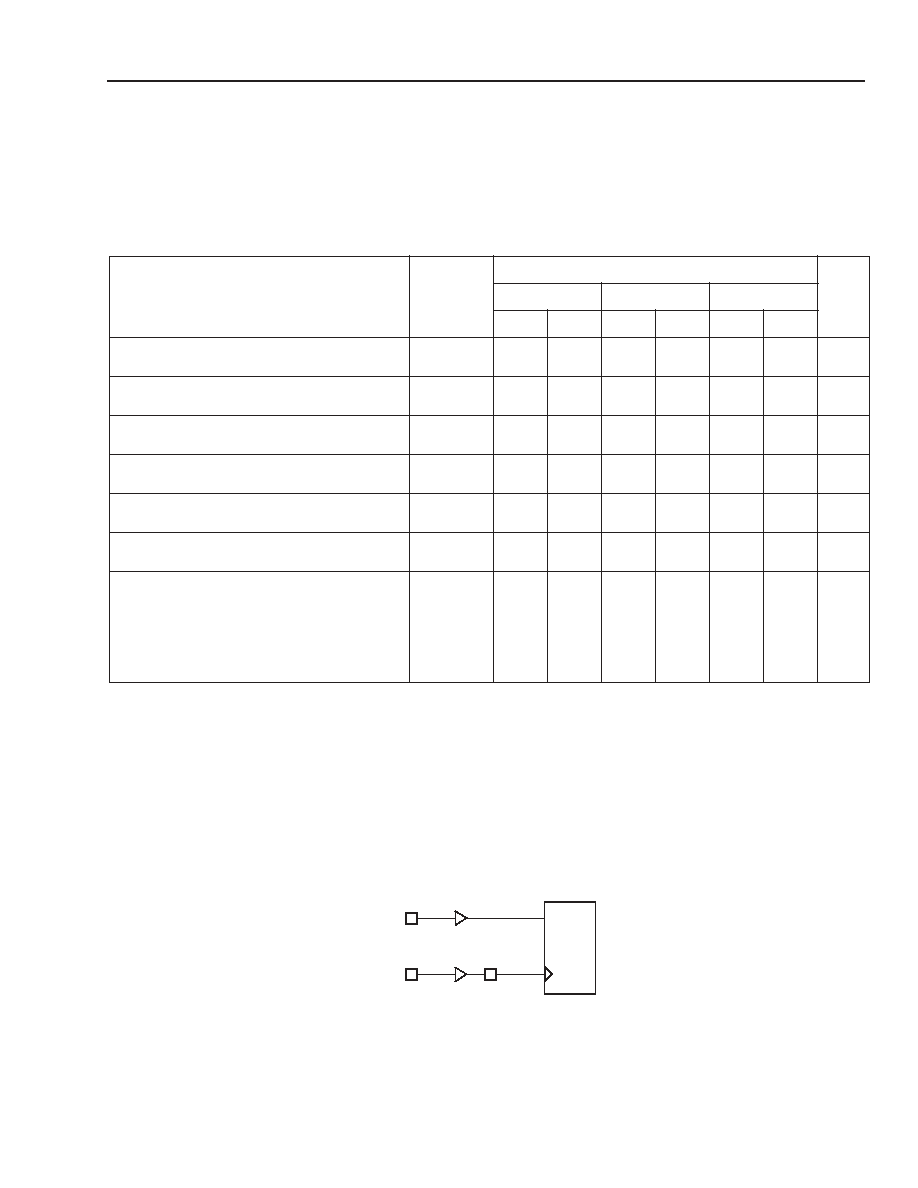
Lattice Semiconductor
87
Data Sheet
March, 2003
ORCA
Series 4 FPGAs
Timing Characteristics
(continued)
Table 49. Secondary CLK (SCLK) Setup/Hold Time without on-chip PLLs (Pin-to-Pin)
OR4Exx commercial: VDD15 = 1.425 V to 1.575 V, VDD33 = 3.0 V to 3.6 V, VDDIO = 3.0 V to 3.6 V, �40 �C
<
TJ
<
+85 �C
OR4Exx industrial: VDD15 = 1.425 V to 1.575 V, VDD33 = 3.0 V to 3.6 V, VDDIO = 3.0 V to 3.6 V, �40 �C
<
TJ
<
+100 �C
Notes:
1. The pin-to-pin timing parameters in this table will match ispLEVER if the clock delay multiplier in the setup preference is set to 0.95 for setup
time and 1.05 for hold time.
2. Timing is without the use of the phase-locked loops (PLLs) or PIO input FF cycle stealing delays (which can provide reductions in setup time
at the expense of hold time).
3. This setup/hold time is for a fully routed clock tree that uses the secondary clock network. It includes both the LVTTL (3.3 V) input clock buffer
delay, the clock routing to the PIO CLK input, the setup/hold time of the PIO FF (with the data input delay disabled) and the
LVTTL (3.3 V) input data buffer to PIO FF delay. An SCLK input clock can be at any input pin.
4. For timing improvements using other I/O buffer types for the input clock buffer or input data buffer, see Table 53.
5. The ORT8850H FPSC has slightly reduced performance from the values in this table. ispLEVER will report the actual delay values for all
devices, including the ORT8850H in this arrangement.
5-4847(F).b
Figure 49. Input to Secondary CLK Setup/Hold Time
Description
Device
Speed
Unit
-1
-2
-3
Min
Max
Min
Max
Min
Max
Input to SCLK Setup Time (Input within 6
PICs of SCLK input), Fast Capture Enabled
All
5.95
--
5.54
--
5.06
--
ns
Input to SCLK Setup Time (Input within 6
PICs of SCLK input), No Input Data Delay
All
0.00
--
0.00
--
0.00
--
ns
Reduced Setup Time per each extra 6 PICs
per clock route direction.
All
0.36
--
0.38
--
0.34
--
ns
Input to SCLK Hold Time (Input within 6
PICs of SCLK input), Fast Capture Enabled
All
0.00
--
0.00
--
0.00
--
ns
Input to SCLK Hold Time (Input within 6
PICs of SCLK input), No Input Data Delay
All
3.07
--
3.04
--
2.74
--
ns
Additional Hold Time per each extra 6 PICs
per clock route direction.
All
0.36
--
0.38
--
0.34
--
ns
Input Delay Adjustments from PIO Cycle
Stealing (typically used to reduce setup time
by the min value shown):
One Delay Cell
Two Delay Cells
Three Delay Cells
ICYCDEL1
ICYCDEL2
ICYCDEL3
--
--
--
0.89
1.64
2.43
--
--
--
0.70
1.29
1.98
--
--
--
0.64
1.18
1.80
ns
ns
ns
Q
D
SCLK
INPUT
PIO FF

88
Lattice Semiconductor
Data Sheet
March, 2003
ORCA
Series 4 FPGAs
Timing Characteristics
(continued)
Table 50. Edge CLK (ECLK) Setup/Hold Time without on-chip PLLs (Pin-to-Pin)
OR4Exx commercial: V
DD
15 = 1.425 V to 1.575 V, V
DD
33 = 3.0 V to 3.6 V, V
DD
IO = 3.0 V to 3.6 V, �40 �C
<
T
J
<
+85
�C
OR4Exx industrial: V
DD
15 = 1.425 V to 1.575 V, V
DD
33 = 3.0 V to 3.6 V, V
DD
IO = 3.0 V to 3.6 V, �40 �C
<
T
J
<
+100
�C
Notes:
1. The pin-to-pin timing parameters in this table will match ispLEVER if the clock delay multiplier in the setup preference is set to 0.95 for setup
time and 1.05 for hold time.
2. Timing is without the use of the phase-locked loops (PLLs) or PIO input FF cycle stealing delays (which can provide reductions in setup time
at the expense of hold time).
3. This setup/hold time is for a fully routed clock tree that uses the Edge Clock network. It includes both the LVTTL (3.3 V) input clock buffer
delay, the clock routing to the PIO CLK input, the setup/hold time of the PIO FF (with the data input delay disabled) and the LVTTL (3.3 V)
input data buffer to PIO FF delay. Edge clocks can only be connected to one pin or pin-pair per PIC, those ending in the letter C for singled-
ended and those ending in C and D for differential inputs. See the pinout section for more details.
4. For timing improvements using other I/O buffer types for the input clock buffer or input data buffer, see Table 53.
5. The ORT8850H FPSC has slightly reduced performance from the values in this table. ispLEVER will report the actual delay values for all
devices, including the ORT8850H in this arrangement.
5-4847(F).b
Figure 50. Input to Edge CLK Setup/Hold Time
Description
Device
Speed
Unit
-1
-2
-3
Min
Max
Min
Max
Min
Max
Input to ECLK Setup Time (Input within 6
PICs of ECLK input), Fast Capture Enabled
All
1.13
--
1.17
--
1.08
--
ns
Input to ECLK Setup Time (Input within 6
PICs of ECLK input), Fast Input Enabled
All
0.00
--
0.00
--
0.00
--
ns
Reduced Setup Time per each extra 6 PICs
per clock route direction.
All
0.36
--
0.38
--
0.34
--
ns
Input to ECLK Hold Time (Input within 6 PICs
of ECLK input), Fast Capture Enabled
All
0.00
--
0.00
--
0.00
--
ns
Input to ECLK Hold Time (Input within 6 PICs
of ECLK input), Fast Input Enabled
All
2.68
--
2.65
--
2.40
--
ns
Additional Hold Time per each extra 6 PICs
per clock route direction.
All
0.36
--
0.38
--
0.34
--
ns
Input Delay Adjustments from PIO Cycle
Stealing (typically used to reduce setup time
by the min value shown):
One Delay Cell
Two Delay Cells
Three Delay Cells
ICYCDEL1
ICYCDEL2
ICYCDEL3
--
--
--
0.89
1.64
2.43
--
--
--
0.70
1.29
1.98
--
--
--
0.64
1.18
1.80
ns
ns
ns
Q
D
ECLK
INPUT
PIO FF
Lattice Semiconductor
89
Data Sheet
March, 2003
ORCA
Series 4 FPGAs
Timing Characteristics
(continued)
Table 51. Primary CLK (PCLK) Setup/Hold Time without on-chip PLLs (Pin-to-Pin)
OR4Exx commercial: V
DD
15 = 1.425 V to 1.575 V, V
DD
33 = 3.0 V to 3.6 V, V
DD
IO = 3.0 V to 3.6 V, �40 �C
<
T
J
<
+85
�C
OR4Exx industrial: V
DD
15 = 1.425 V to 1.575 V, V
DD
33 = 3.0 V to 3.6 V, V
DD
IO = 3.0 V to 3.6 V, �40 �C
<
T
J
<
+100
�C
Notes:
1. The pin-to-pin timing parameters in this table will match ispLEVER if the clock delay multiplier in the setup preference is set to 0.95 for setup
time and 1.05 for hold time.
2. Timing is without the use of the phase-locked loops (PLLs) or PIO input FF cycle stealing delays (which can provide reductions in setup time
at the expense of hold time).
3. This setup/hold time is for a fully routed clock tree that uses the primary clock network. It includes both the LVTTL (3.3 V) input clock buffer
delay, the clock routing to the PIO CLK input, the setup/hold time of the PIO FF (with the data input delay disabled) and the LVTTL (3.3 V)
input data buffer to PIO FF delay. The PCLK input clock is connected at the semi-dedicated primary clock input pins.
4. For timing improvements using other I/O buffer types for the input clock buffer or input data buffer, see Table 53.
5-4847(F).a
Figure 51. Input to Primary Clock Setup/Hold Time
Description
Device
Speed
Unit
-1
-2
-3
Min
Max
Min
Max
Min
Max
Input to PCLK Setup Time, Input Data Delay
Enabled
OR4E02
OR4E04
OR4E06
4.37
4.19
4.06
--
--
--
4.36
4.21
4.09
--
--
--
3.99
3.85
3.75
--
--
--
ns
ns
ns
Input to PCLK Setup Time, No Input Data
Delay
OR4E02
OR4E04
OR4E06
0.00
0.00
0.00
--
--
--
0.00
0.00
0.00
--
--
--
0.00
0.00
0.00
--
--
--
ns
ns
ns
Input to PCLK Hold Time, Input Data Delay
Enabled
OR4E02
OR4E04
OR4E06
0.00
0.00
0.00
--
--
--
0.00
0.00
0.00
--
--
--
0.00
0.00
0.00
--
--
--
ns
ns
ns
Input to PCLK Hold Time, No Input Data
Delay
OR4E02
OR4E04
OR4E06
4.93
5.17
5.38
--
--
--
4.45
4.66
4.84
--
--
--
4.02
4.21
4.37
--
--
--
ns
ns
ns
Input Delay Adjustments from PIO Cycle
Stealing (typically used to reduce setup time
by the min value shown):
One Delay Cell
Two Delay Cells
Three Delay Cells
ICYCDEL1
ICYCDEL2
ICYCDEL3
--
--
--
0.89
1.64
2.43
--
--
--
0.70
1.29
1.98
--
--
--
0.64
1.18
1.80
ns
ns
ns
Q
D
PCLK
INPUT
PIO FF
90
Lattice Semiconductor
Data Sheet
March, 2003
ORCA
Series 4 FPGAs
Timing Characteristics
(continued)
Table 52. Primary CLK (PCLK) Setup/Hold Time using on-chip PLLs (Pin-to-Pin)
OR4Exx commercial: VDD15 = 1.425 V to 1.575 V, VDD33 = 3.0 V to 3.6 V, VDDIO = 3.0 V to 3.6 V, �40 �C
<
TJ
<
+85 �C
OR4Exx industrial: VDD15 = 1.425 V to 1.575 V, VDD33 = 3.0 V to 3.6 V, VDDIO = 3.0 V to 3.6 V, �40 �C
<
TJ
<
+100 �C
Notes:
1. The pin-to-pin timing parameters in this table will match ispLEVER if the clock delay multiplier in the setup preference is set to 0.95 for setup
time and 1.05 for hold time.
2. Timing uses the automatic delay compensation mode of the PLLs. The feedback to the PLL is provided by the global system clock routing.
Other delay values are possible by using the phase modifications mode of the PLL instead.
3. This setup/hold time is for a fully routed clock tree that uses the primary clock network. It includes both the LVTTL (3.3 V) input clock buffer
delay, PLL block, the clock routing to the PIO CLK input, the setup/hold time of the PIO FF (with the data input delay disabled) and the
LVTTL (3.3 V) input data buffer to PIO FF delay. The PCLK input clock is connected at the semi-dedicated PLL input pin.
4. Note that the PIO cycle stealing delay adjustments and the PLL cycle stealing delay adjustments are each attempting to pull the same clock
in both directions. If both are being used, then the difference between them will provide the basis for PIO setup and hold times.
5. For timing improvements using other I/O buffer types for the input clock buffer or input data buffer, see Table 53.
Description
Device
Speed
Unit
-1
-2
-3
Min Max Min Max Min Max
Input to PCLK Setup Time, Input Data Delay Enabled
All
7.73
--
7.30
--
6.66
--
ns
Input to PCLK Setup Time, No Input Data Delay
All
0.00
--
0.00
--
0.00
--
ns
Input to PCLK Hold Time, Input Data Delay Enabled
All
0.00
--
0.00
--
0.00
--
ns
Input to PCLK Hold Time, No Input Data Delay
All
1.82
--
1.73
--
1.57
--
ns
Input Delay Adjustments from PIO Cycle Stealing
(typically used to reduce setup time by the min value
shown):
One Delay Cell
Two Delay Cells
Three Delay Cells
ICYCDEL1
ICYCDEL2
ICYCDEL3
--
--
--
0.89
1.64
2.43
--
--
--
0.70
1.29
1.98
--
--
--
0.64
1.18
1.80
ns
ns
ns
PLL Delay Adjustments from Cycle Stealing (used to
reduce hold by the min delay value shown):
One Delay Cell
Two Delay Cells
Three Delay Cells
PLLCDEL1
PLLCDEL2
PLLCDEL3
--
--
--
0.89
1.64
2.43
--
--
--
0.70
1.29
1.98
--
--
--
0.64
1.18
1.80
ns
ns
ns
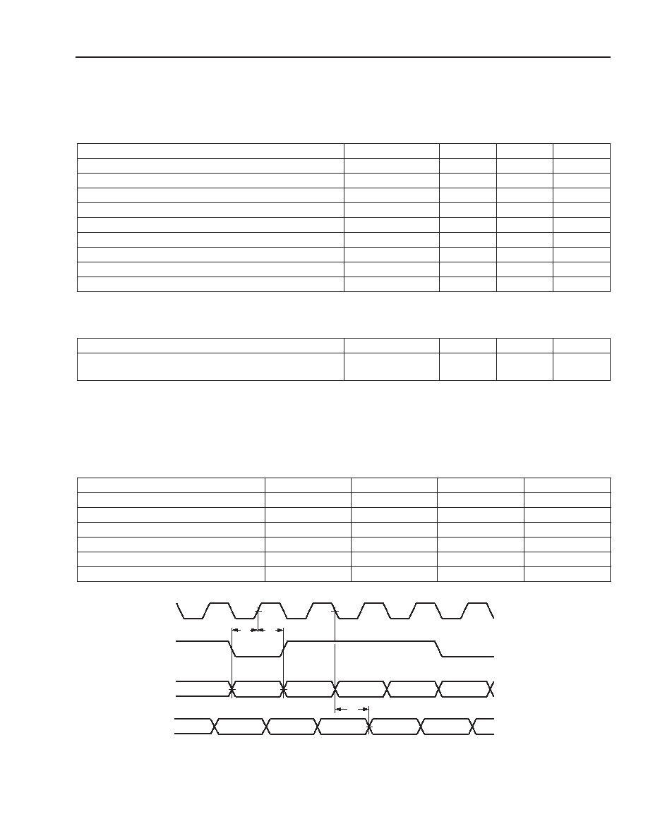
Lattice Semiconductor
91
Data Sheet
March, 2003
ORCA
Series 4 FPGAs
Timing Characteristics
(continued)
Table 53. Microprocessor Interface (MPI) Timing Characteristics
OR4Exx commercial/industrial: VDD15 = 1.4 V to 1.6 V, VDD33 = 3.0 V to 3.6 V, VDDIO= 3.0 V to 3.6 V, �40 �C
<
TJ
<
+ 125 �C
Table 54. Embedded System Bus (ESB) Timing Characteristics
OR4Exx commercial/industrial: VDD15 = 1.4 V to 1.6 V, VDD33 = 3.0 V to 3.6 V, VDDIO= 3.0 V to 3.6 V, �40 �C
<
TJ
<
+ 125 �C
Table 55. Phase-Locked Loop (PLL) Timing Characteristics
See the section on PLLs in this data sheet and in the PLL application note for timing information.
Table 56. Boundary-Scan Timing Characteristics
OR4Exx commercial/industrial: VDD15 = 1.4 V to 1.6 V, VDD33 = 3.0 V to 3.6 V, VDDIO= 3.0 V to 3.6 V, �40 �C
<
TJ
<
+125 �C;
CL = 30 p
F.
5-6764(F)
Figure 52. Boundary-Scan Timing Diagram
Parameter
Symbol
Min
Max
Unit
MPI Control (STRB, WR, etc.) to MPI_CLK Setup Time
MPICTRL_SET
7.7
--
ns
MPI Address to MPI_CLK Setup Time
MPIADR_SET
3.5
--
ns
MPI Write Data to MPI_CLK Setup Time
MPIDAT_SET
3.4
--
ns
All Hold Times
MPI_HLD
0.0
--
ns
MPI_CLK to MPI Control (TA, TEA, RETRY)
MPICTRL_DEL
--
8.3
ns
MPI_CLK to MPI Data (8-bit)
MPIDAT8_DEL
--
9.2
ns
MPI_CLK to MPI Data (16-bit)
MPIDAT16_DEL
--
10.0
ns
MPI_CLK to MPI Data (32-bit)
MPIDAT32_DEL
--
10.6
ns
MPI_CLK Frequency
MPI_CLK_FRQ
--
66
MHz
Parameter
Symbol
Min
Max
Unit
ESB_CLK Frequency (no wait states)
ESB_CLK Frequency (with wait states)
ESB_CLK_FRQ
ESB_CLK_FRQ
--
--
66
100
MHz
MHz
Parameter
Symbol
Min
Max
Unit
TDI/TMS to TCK Setup Time
T
S
10.0
--
ns
TDI/TMS Hold Time from TCK
T
H
0.0
--
ns
TCK Low Time
T
CL
25.0
--
ns
TCK High Time
T
CH
25.0
--
ns
TCK to TDO Delay
T
D
--
10.0
ns
TCK Frequency
T
TCK
--
20.0
MHz
TCK
TMS
TDI
TDO
T
S
T
H
T
D
92
Lattice Semiconductor
Data Sheet
March, 2003
ORCA
Series 4 FPGAs
Timing Characteristics
(continued)
Configuration Timing
Table 57. General Configuration Mode Timing Characteristics
OR4Exx commercial/industrial: VDD15 = 1.4 V to 1.6 V, VDD33 = 3.0 V to 3.6 V, VDDIO = 3.0 V to 3.6 V, �40 �C
<
TJ
<
+125 �C;CL = 30 pF
* Not applicable to asynchronous peripheral mode.
Values are shown for the MPI in 32-bit mode with daisy-chaining through the DOUT pin disabled.
Parameter
Symbol
Min
Max
Unit
All Configuration Modes
M[3:0] Setup Time to INIT High
TSMODE
0.00
--
ns
M[3:0] Hold Time from INIT High
THMODE
600.00
--
ns
RESET Pulse Width Low to Start Reconfiguration
TRW
50.00
--
ns
PRGM Pulse Width Low to Start Reconfiguration
TPGW
50.00
--
ns
Master and Asynchronous Peripheral Modes
Power-on Reset Delay
CCLK Period (M3 = 0)
(M3 = 1)
Configuration Latency (autoincrement mode, no EBR initialization):
OR4E02
(M3 = 0)
(M3 = 1)
OR4E04
(M3 = 0)
(M3 = 1)
OR4E06
(M3 = 0)
(M3 = 1)
TPO
TCCLK
TCL
15.70
60.00
480.00
69.7
557.6
187.7
1,501.5
284.2
2,273.9
52.40
200.00
1,600.00
232.3
1,858.6
625.6
5,004.9
947.5
7,579.7
ms
ns
ns
ms
ms
ms
ms
ms
ms
Microprocessor (MPI) Mode
Power-on Reset Delay
MPI Clock Period
Configuration Latency (autoincrement mode, no EBR initialization):
OR4E02
OR4E04
OR4E06
TPO
TCL
15.70
15.00
290,412
782,018
1,184,322
52.40
--
--
--
--
ms
MPI clk cycles
MPI clk cycles
MPI clk cycles
Partial Reconfiguration (per data frame):
OR4E02
OR4E04
OR4E06
TPR
225
321
385
--
--
--
MPI clk cycles
MPI clk cycles
MPI clk cycles
Slave Serial Mode
Power-on Reset Delay
CCLK Period
Configuration Latency (autoincrement mode, no EBR initialization):
OR4E02
OR4E04
OR4E06
TPO
TCCLK
TCL
3.90
10.00
11.6
31.3
47.4
13.10
--
--
--
--
ms
ns
ms
ms
ms
Partial Reconfiguration (per data frame):
OR4E02
OR4E04
OR4E06
TPR
9.0
12.8
15.4
--
--
--
�s
�s
�s
Lattice Semiconductor
93
Data Sheet
March, 2003
ORCA
Series 4 FPGAs
Timing Characteristics
(continued)
Table 58. General Configuration Mode Timing Characteristics (continued)
OR4Exx commercial/industrial: VDD15 = 1.4 V to 1.6 V, VDD33 = 3.0 V to 3.6 V, VDDIO = 3.0 V to 3.6 V, �40 �C
<
TJ
<
+125 � C;CL = 30 pF
.
Note: T
PO
is triggered when V
DD
33 reaches between 2.7 V and 3.0 V.
Parameter
Symbol
Min
Max
Unit
Slave Parallel Mode
Power-on Reset Delay
CCLK Period:
Configuration Latency (normal mode):
OR4E02
OR4E04
OR4E06
TPO
TCCLK
TCL
3.90
10.00
1.5
3.9
5.9
13.10
--
--
--
--
ms
ns
ms
ms
ms
Partial Reconfiguration (per data frame):
OR4E02
OR4E04
OR4E06
TPR
1.1
1.6
1.9
--
--
--
�s
�s
�s
INIT Timing
INIT High to CCLK Delay:
Slave Parallel
Slave Serial
Master Serial
Master Parallel
TINIT_CCLK
0.50
0.50
0.50
0.50
1.60
1.60
1.60
1.60
�s
�s
�s
�s
Initialization Latency (PRGM high to INIT high):
OR4E02
OR4E04
OR4E06
TIL
0.43
0.58
0.74
1.44
1.95
2.46
ms
ms
ms
INIT High to WR, Asynchronous Peripheral
TINIT_WR
2.00
--
�s

94
Lattice Semiconductor
Data Sheet
March, 2003
ORCA
Series 4 FPGAs
Timing Characteristics
(continued)
5-4531(F).a
Figure 53. General Configuration Mode Timing Diagram
V
DD
15, V
DD
33
CCLK
M[3:0]
PRGM
INIT
T
PO
+ T
IL
T
IL
T
CCLK
T
SMODE
T
HMODE
T
INIT_CLK
DONE
T
CL
T
PGW
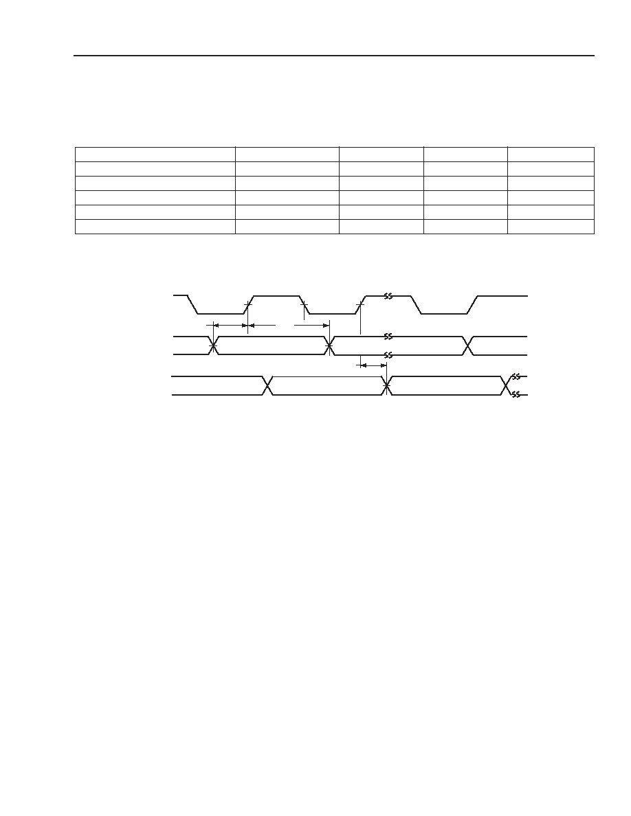
Lattice Semiconductor
95
Data Sheet
March, 2003
ORCA
Series 4 FPGAs
Timing Characteristics
(continued)
Table 59. Master Serial Configuration Mode Timing Characteristics
OR4Exx commercial/industrial: VDD15 = 1.4 V to 1.6 V, VDD33 = 3.0 V to 3.6 V, VDDIO = 3.0 V to 3.6 V, �40 �C < TJ < +125 �C;
CL = 30 pF.
Note: Serial configuration data is transmitted out on DOUT on the rising edge of CCLK after it is input on DIN.
* Data gets clocked out from an external serial ROM. The clock to data delay of the serial ROM must be less than the CCLK frequency since
the data available out of the serial ROM must be setup and waiting to be clocked into the FPGA before the next CCLK rising edge.
5-4532(F).b
Figure 54. Master Serial Configuration Mode Timing Diagram
Parameter
Symbol
Min
Max
Unit
DIN Setup Time*
T
S
10.00
--
ns
DIN Hold Time
T
H
0.00
--
ns
CCLK Frequency (M3 = 0)
F
C
5.00
16.67
MHz
CCLK Frequency (M3 = 1)
F
C
0.63
2.08
MHz
CCLK to DOUT Delay
T
D
--
5.00
ns
DIN
CCLK
DOUT
T
S
T
H
BIT N
BIT N
T
D
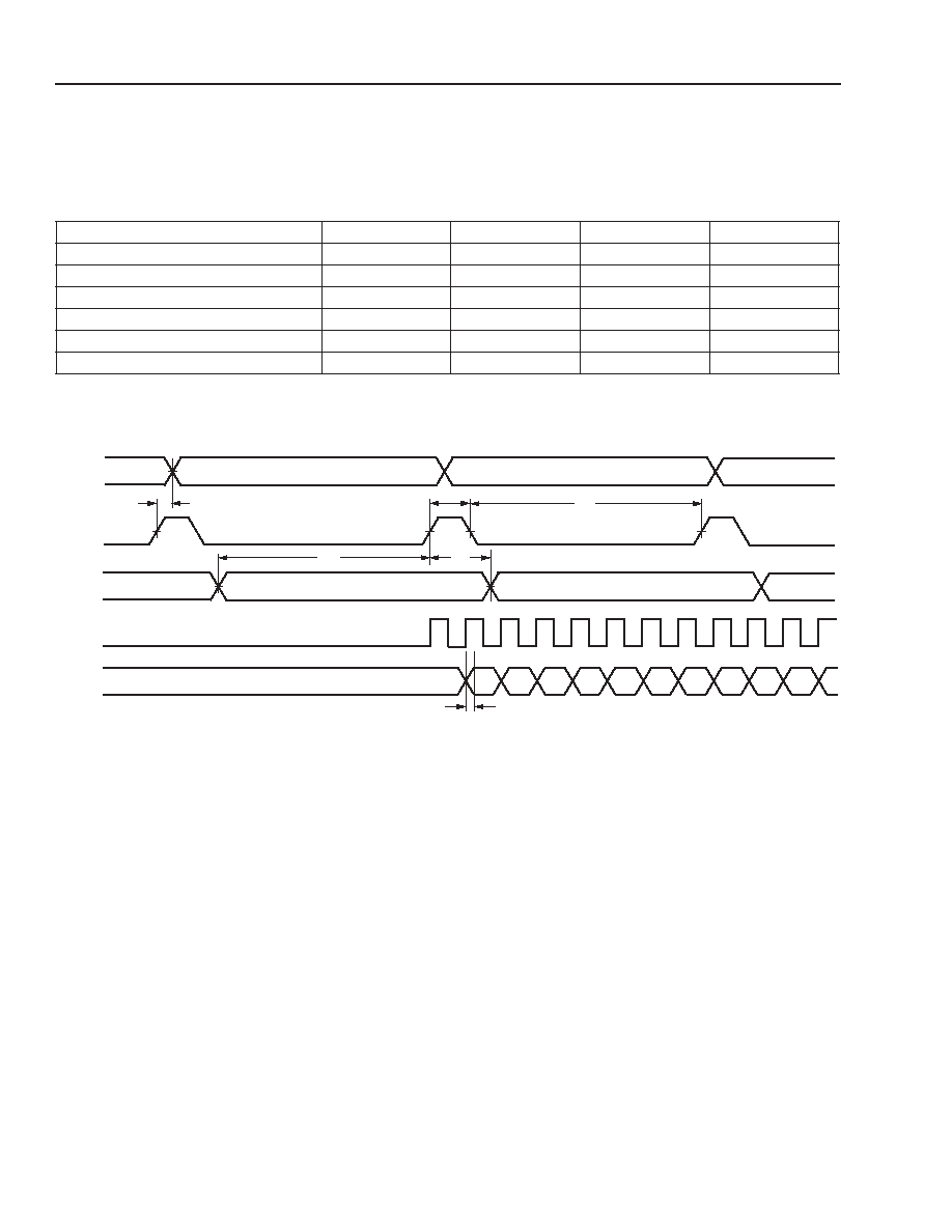
96
Lattice Semiconductor
Data Sheet
March, 2003
ORCA
Series 4 FPGAs
Timing Characteristics
(continued)
Table 60. Master Parallel Configuration Mode Timing Characteristics
OR4Exx commercial/industrial: VDD15 = 1.4 V to 1.6 V, VDD33 = 3.0 V to 3.6 V, VDDIO = 3.0 V to 3.6 V, �40 �C < TJ <
+125 �C; CL = 30 pF.
Note:
The RCLK period consists of seven CCLKs for RCLK low and one CCLK for RCLK high.
Serial data is transmitted out on DOUT two CCLK cycles after the byte is input on D[7:0].
2706(F)
Figure 55. Master Parallel Configuration Mode Timing Diagram
Parameter
Symbol
Min
Max
Unit
RCLK to Address Valid
T
AV
--
10.00
ns
D[7:0] Setup Time to RCLK High
T
S
10.00
--
ns
D[7:0] Hold Time to RCLK High
T
H
0.00
--
ns
RCLK Low Time
T
CL
7.00
7.00
CCLK cycles
RCLK High Time
T
CH
1.00
1.00
CCLK cycles
CCLK to DOUT
T
D
--
5.00
ns
A[21:0]
RCLK
D[7:0]
T
CL
T
CH
T
AV
CCLK
DOUT
T
H
T
S
BYTE N
BYTE N + 1
D0
D1
D2
D3
D4
D5
D6
D7
T
D
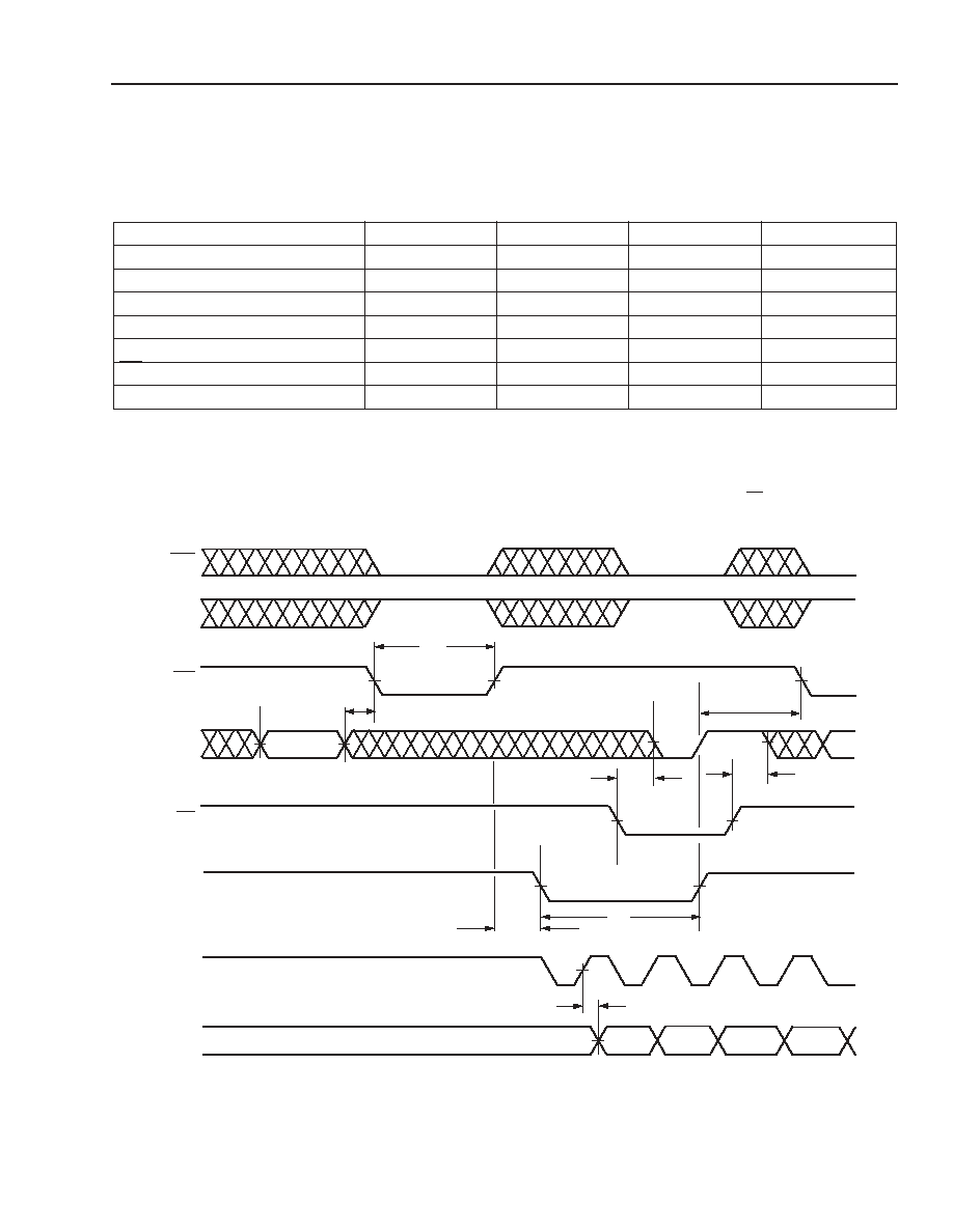
Lattice Semiconductor
97
Data Sheet
March, 2003
ORCA
Series 4 FPGAs
Timing Characteristics
(continued)
Table 61. Asynchronous Peripheral Configuration Mode Timing Characteristics
OR4Exx commercial/industrial: VDD15 = 1.4 V to 1.6 V, VDD33 = 3.0 V to 3.6 V, VDDIO = 3.0 V to 3.6 V, �40 �C < TJ <
+125 �C; CL = 30 pF.
* The smaller delay is for fast asynchronous peripheral mode (mode pins M[3:0]="0101") and the larger delay is for slow asynchronous periph-
eral mode (mode pins M[3:0]="1101").
This parameter is valid whether the end of not RDY is determined from the RDY pin or from the D7 pin.
Note: Serial data is transmitted out on DOUT on the rising edge of CCLK after the byte is input on D[7:0].
D[2:0] timing is the same as the write data portion of the D[7:3] waveform because D[2:0] are not enabled by
RD.
5-4533(F).b
Figure 56. Asynchronous Peripheral Configuration Mode Timing Diagram
Parameter
Symbol
Min
Max
Unit
WR, CS0, and CS1 Pulse Width
TWR
10.00
60.00 / 500.00*
ns
D[7:0] Setup Time:
TS
0.00
--
ns
RDY Delay
TRDY
--
10.00
ns
RDY Low
TB
1.00
8.00
CCLK Periods
Earliest WR After RDY Goes High
TWR2
0.00
--
ns
RD to D[7:0] Enable/Disable
TDEN
--
10.00
ns
CCLK to DOUT
TD
--
5.00
ns
CS1
D[7:3]
CCLK
DOUT
CS0
RDY
D0
D1
D2
T
B
T
WR
T
S
T
RDY
WR
D7
T
D
PREVIOUS BYTE
T
WR2
WRITE DATA
D3
T
DEN
T
DEN
RD

98
Lattice Semiconductor
Data Sheet
March, 2003
ORCA
Series 4 FPGAs
Timing Characteristics
(continued)
Table 62. Slave Serial Configuration Mode Timing Characteristics
OR4Exx commercial/industrial: VDD15 = 1.4 V to 1.6 V, VDD33 = 3.0 V to 3.6 V, VDDIO = 3.0 V to 3.6 V, �40 �C < TJ
< +125 �C; CL = 30 pF.
Note: Serial configuration data is transmitted out on DOUT on the rising edge of CCLK after it is input on DIN.
5-4535(F).b
Figure 57. Slave Serial Configuration Mode Timing Diagram
Parameter
Symbol
Min
Max
Unit
DIN Setup Time
T
S
5.00
--
ns
DIN Hold Time
T
H
0.00
--
ns
CCLK High Time
T
CH
5.00
--
ns
CCLK Low Time
T
CL
5.00
--
ns
CCLK Frequency
F
C
--
100.00
MHz
CCLK to DOUT
T
D
--
5.00
ns
DIN
CCLK
DOUT
T
D
T
S
T
H
T
CL
T
CH
BIT N
BIT N
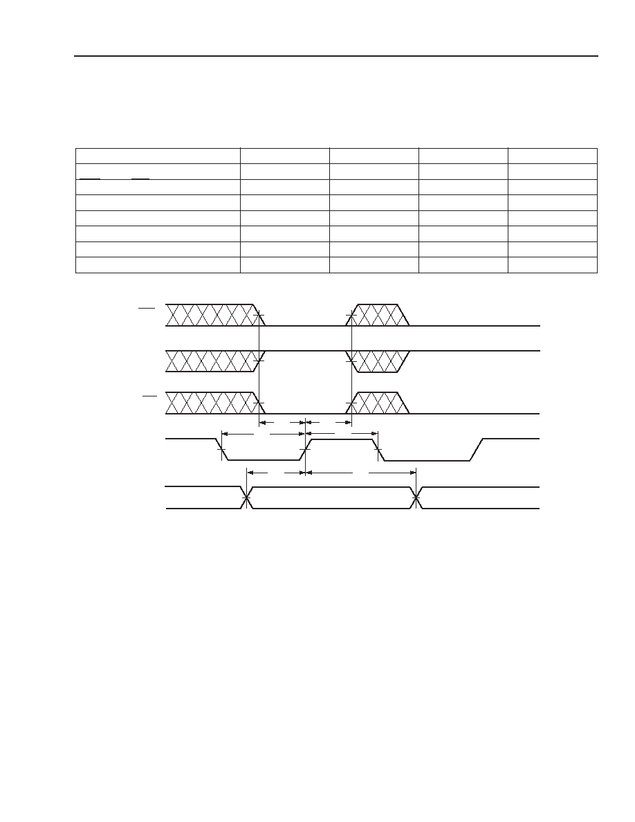
Lattice Semiconductor
99
Data Sheet
March, 2003
ORCA
Series 4 FPGAs
Timing Characteristics
(continued)
Table 63. Slave Parallel Configuration Mode Timing Characteristics
OR4Exx commercial/industrial: VDD15 = 1.4 V to 1.6 V, VDD33 = 3.0 V to 3.6 V, VDDIO = 3.0 V to 3.6 V, �40 �C < TJ < +125 �C;
CL = 30 pF.
Note: Daisy-chaining of FPGAs is not supported in this mode.
5-2848(F)
Figure 58. Slave Parallel Configuration Mode Timing Diagram
Parameter
Symbol
Min
Max
Unit
CS0, CS1, WR Setup Time
TS1
5.00
--
ns
CS0, CS1, WR Hold Time
TH1
2.00
--
ns
D[7:0] Setup Time
TS2
5.00
--
ns
D[7:0] Hold Time
TH2
0.00
--
ns
CCLK High Time
TCH
5.00
--
ns
CCLK Low Time
TCL
5.00
--
ns
CCLK Frequency
FC
--
100.00
MHz
T
S1
T
S2
T
H2
CS1
CCLK
D[7:0]
CS0
WR
T
CL
T
CH
T
H1

100
Lattice Semiconductor
Data Sheet
March, 2003
ORCA
Series 4 FPGAs
Timing Characteristics
(continued)
Readback Timing
Table 64. Readback Timing Characteristics
OR4Exx commercial/industrial: VDD15 = 1.4 V to 1.6 V, VDD33 = 3.0 V to 3.6 V, VDDIO = 3.0 V to 3.6 V, �40 �C < TJ
< +125 �C; CL = 30 pF.
5-4536(F)
Figure 59. Readback Timing Diagram
Parameter
Symbol
Min
Max
Unit
RD_CFG
to CCLK Setup Time
T
S
5.00
--
ns
RD_CFG
High Width to Abort Readback
T
RBA
2
--
CCLK cycles
CCLK Low Time
T
CL
5.00
--
ns
CCLK High Time
T
CH
5.00
--
ns
CCLK Frequency
F
C
--
100.00
MHz
CCLK to RD_DATA Delay
T
D
--
5.00
ns
T
D
T
CH
CCLK
RD_DATA
T
S
T
CL
RD_CFG
BIT 0
BIT 1
BIT 0
T
RBA
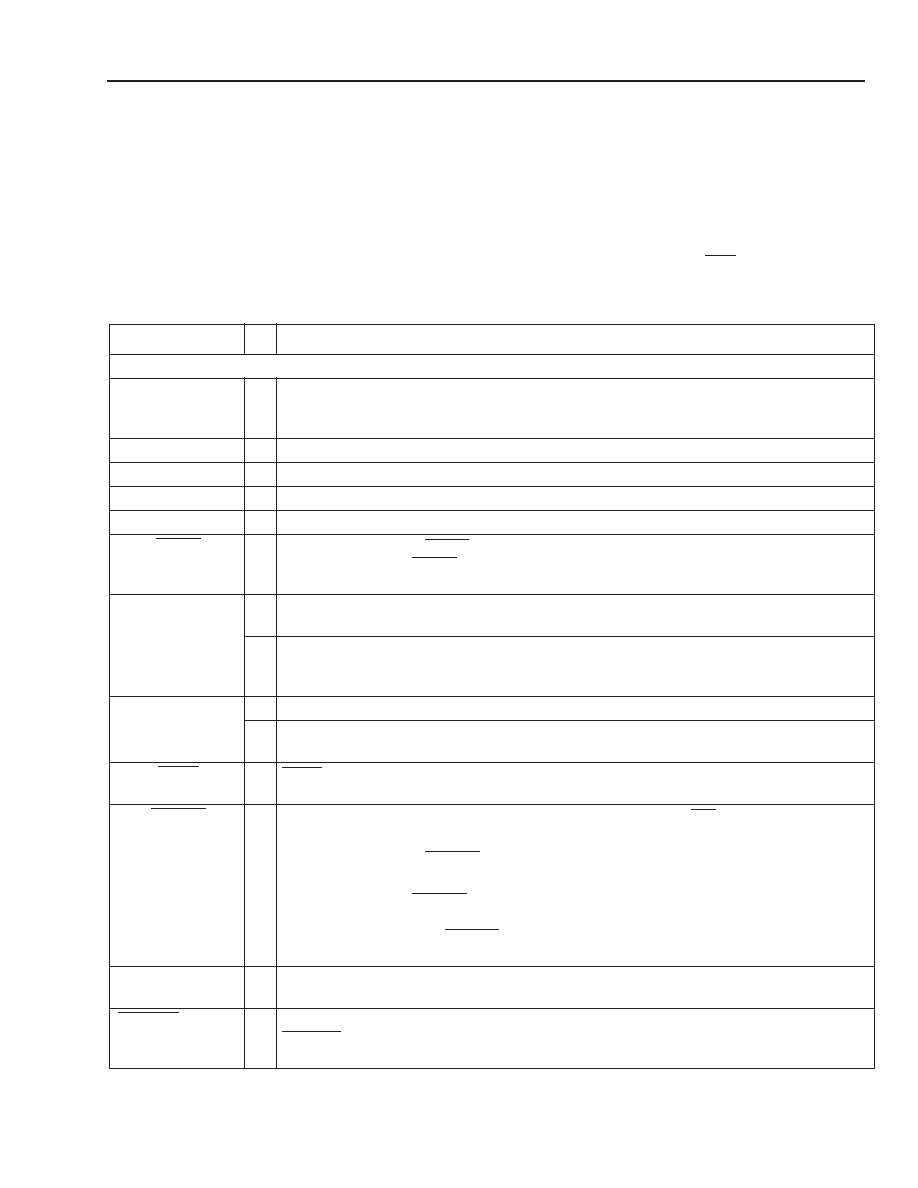
Lattice Semiconductor
101
Data Sheet
March, 2003
ORCA
Series 4 FPGAs
Pin Information
Pin Descriptions
This section describes the pins found on the Series 4 FPGAs. Any pin not described in this table is a user-program-
mable I/O. During configuration, the user-programmable I/Os are 3-stated with an internal pull-up resistor enabled.
If any pin is not used (or not bonded to a package pin), it is also 3-stated with an internal pull-up resistor enabled
after configuration. The pin descriptions in Table 65 and throughout this data sheet show active-low signals with an
overscore. The package pinout tables that follow, show this as a signal ending with _N, for LDC and LDC_N are
equivalent.
Table 65. Pin Descriptions
Symbol
I/O
Description
Dedicated Pins
V
DD
33
-- 3.3 V positive power supply. This power supply is used for 3.3 V configuration RAMs and
internal PLLs. When using PLLs, this power supply should be well isolated from all other
power supplies on the board for proper operation.
V
DD
15
-- 1.5 V positive power supply for internal logic.
V
DD
IO
-- Positive power supply used by I/O banks.
V
SS
-- Ground.
PTEMP
I
Temperature sensing diode pin. Dedicated input.
RESET
I
During configuration,
RESET
forces the restart of configuration and a pull-up is enabled.
After configuration,
RESET
can be used as a general FPGA input or as a direct input,
which causes all PLC latches/FFs to be asynchronously set/reset.
CCLK
O In the master and asynchronous peripheral modes, CCLK is an output which strobes con-
figuration data in.
I
In the slave or readback after configuration, CCLK is input synchronous with the data on
DIN or D[7:0]. CCLK is an output for daisy-chain operation when the lead device is in
master, peripheral, or system bus modes.
DONE
I
As an input, a low level on DONE delays FPGA start-up after configuration.*
O As an active-high, open-drain output, a high level on this signal indicates that configura-
tion is complete. DONE has an optional pull-up resistor.
PRGM
I
PRGM
is an active-low input that forces the restart of configuration and resets the bound-
ary-scan circuitry. This pin always has an active pull-up.
RD_CFG
I
This pin must be held high during device initialization until the
INIT
pin goes high. This pin
always has an active pull-up.
During configuration,
RD_CFG
is an active-low input that activates the TS_ALL function
and 3-states all of the I/O.
After configuration,
RD_CFG
can be selected (via a bit stream option) to activate the
TS_ALL function as described above, or, if readback is enabled via a bit stream option, a
high-to-low transition on
RD_CFG
will initiate readback of the configuration data, including
PFU output states, starting with frame address 0.
RD_DATA/TDO
O RD_DATA/TDO is a dual-function pin. If used for readback, RD_DATA provides configura-
tion data out. If used in boundary-scan, TDO is test data out.
CFG_IRQ/MPI_IRQ
O During JTAG, slave, master, and asynchronous peripheral configuration assertion on this
CFG_IRQ
(active-low) indicates an error or errors for block RAM or FPSC initialization.
MPI
active-low interrupt request output, when the MPI is used.
* The FPGA States of Operation section contains more information on how to control these signals during start-up. The timing of DONE release
is controlled by one set of bit stream options, and the timing of the simultaneous release of all other configuration pins (and the activation of all
user I/Os) is controlled by a second set of options.
102
Lattice Semiconductor
Data Sheet
March, 2003
ORCA
Series 4 FPGAs
Pin Information
(continued)
Table 65. Pin Descriptions (continued)
Symbol
I/O
Description
Special-Purpose Pins
M[3:0]
I
During powerup and initialization, M0--M3 are used to select the configuration mode with their val-
ues latched on the rising edge of INIT. During configuration, a pull-up is enabled.
I/O
After configuration, these pins are user-programmable I/O.*
PLL_CK[0:7][TC]
I
Semi-dedicated PLL clock pins. During configuration they are 3-stated with a pull up.
I/O
These pins are user-programmable I/O pins if not used by PLLs after configuration.
P[TBLR]CLK[1:0][TC]
I
Pins dedicated for the primary clock. Input pins on the middle of each side with differential pairing.
I/O
After configuration these pins are user programmable I/O, if not used for clock inputs.
TDI, TCK, TMS
I
Before configuration these pins are test data in, test clock, and test mode select inputs. If bound-
ary-scan is enabled after configuration, these pins remain test data in, test clock, and test mode
select inputs. If boundary-scan is not enabled after configuration, all boundery-scan functions are
inhibited once configuration is complete. During configuration, either TCK or TMS must be held at a
logic 1. Each pin has a pull-up enabled during configuration. To enable boundary-scan after config-
uration, a BNDSCAN library element must be instantiated in the user's design and the appropriate
bitgen setting must be enabled in the ispLEVER software.
I/O
After configuration, these pins are user-programmable I/O in boundary scan is not used.*
RDY/BUSY/RCLK
O
During configuration in asynchronous peripheral mode, RDY/RCLK indicates another byte can be
written to the FPGA. If a read operation is done when the device is selected, the same status is also
available on D7 in asynchronous peripheral mode.
During the master parallel configuration mode, RCLK is a read output signal to an external memory.
This output is not normally used.
I/O
After configuration this pin is a user-programmable I/O pin.*
HDC
O
High during configuration is output high until configuration is complete. It is used as a control output,
indicating that configuration is not complete.
I/O
After configuration, this pin is a user-programmable I/O pin.*
LDC
O
Low during configuration is output low until configuration is complete. It is used as a control output,
indicating that configuration is not complete.
I/O
After configuration, this pin is a user-programmable I/O pin.*
INIT
I/O
INIT is a bidirectional signal before and during configuration. During configuration, a pull-up is
enabled, but an external pull-up resistor is recommended. As an active-low open-drain output, INIT
is held low during power stabilization and internal clearing of memory. As an active-low input, INIT
holds the FPGA in the wait-state before the start of configuration.
After configuration, this pin is a user-programmable I/O pin.*
CS0, CS1
I
CS0 and CS1 are used in the asynchronous peripheral, slave parallel, and microprocessor configu-
ration modes. The FPGA is selected when CS0 is low and CS1 is high. During configuration, a pull-
up is enabled.
I/O
After configuration, if MPI is not used, these pins are user-programmable I/O pins.*
RD/MPI_STRB
I
RD is used in the asynchronous peripheral configuration mode. A low on RD changes D[7:3] into a
status output. WR and RD should not be used simultaneously. If they are, the write strobe overrides.
This pin is also used as the MPI data transfer strobe. As a status indication, a high indicates ready,
and a low indicates busy.
I/O
After configuration, if the MPI is not used, this pin is a user-programmable I/O pin.*
* The FPGA States of Operation section contains more information on how to control these signals during start-up. The timing of DONE release
is controlled by one set of bit stream options, and the timing of the simultaneous release of all other configuration pins (and the activation of all
user I/Os) is controlled by a second set of options.

Lattice Semiconductor
103
Data Sheet
March, 2003
ORCA
Series 4 FPGAs
Pin Information
(continued)
Table 65. Pin Descriptions (continued)
Symbol
I/O
Description
Special-Purpose Pins (continued)
WR/MPI_RW
I
WR is used in asynchronous peripheral mode. A low on WR transfers data on D[7:0] to the
FPGA.
In MPI mode, a high on MPI_RW allows a read from the data bus, while a low causes a write
transfer to the FPGA.
I/O After configuration, if the MPI is not used, WR/MPI_RW is a user-programmable I/O pin.*
PPC_A[14:31]
I
During MPI mode the PPC_A[14:31] are used as the address bus driven by the PowerPC
bus master utilizing the least-significant bits of the PowerPC 32-bit address.
MPI_BURST
I
MPI_BURST is driven low to indicate a burst transfer is in progress in MPI mode. Driven high
indicates that the current transfer is not a burst.
MPI_BDIP
I
MPI_BDIP is driven by the PowerPC processor in MPI mode. Assertion of this pin indicates
that the second beat in front of the current one is requested by the master. Negated before
the burst transfer ends to abort the burst data phase.
MPI_TSZ[0:1]
I
MPI_TSZ[0:1] signals are
driven by the bus master in MPI mode to indicate the data transfer
size for the transaction. Set 01 for byte, 10 for half-word, and 00 for word.
A[21:0]
O During master parallel mode A[21:0] address the configuration EPROMs up to 4M bytes.
I/O If not used for MPI these pins are user-programmable I/O pins after configuration.*
MPI_ACK
O In
MPI
mode this is driven low indicating the MPI received the data on the write cycle or
returned data on a read cycle.
I/O If not used for MPI these pins are user-programmable I/O pins after configuration.*
MPI_CLK
I
This is the PowerPC synchronous, positive-edge bus clock used for the
MPI
interface. It can
be a source of the clock for the embedded system bus. If MPI is used this will be the AMBA
bus clock.
I/O If not used for MPI these pins are user-programmable I/O pins after configuration.*
MPI_TEA
O A low on the MPI transfer error acknowledge indicates that the MPI detects a bus error on
the internal system bus for the current transaction.
I/O If not used for MPI these pins are user-programmable I/O pins after configuration.*
MPI_RTRY
O This pin requests the MPC860 to relinquish the bus and retry the cycle.
I/O If not used for MPI these pins are user-programmable I/O pins after configuration.*
D[0:31]
I/O Selectable data bus width from 8, 16, 32-bit in MPI mode. Driven by the bus master in a write
transaction and driven by MPI in a read transaction.
I
D[7:0] receive configuration data during master parallel, peripheral, and slave parallel config-
uration modes when WR is low and each pin has a pull-up enabled. During serial configura-
tion modes, D0 is the DIN input.
O D[7:3] output internal status for asynchronous peripheral mode when RD is low.
I/O After configuration, if MPI is not used, the pins are user-programmable I/O pins.*
DP[0:3]
I/O Selectable parity bus width in MPI mode from 1, 2, 4-bit, DP[0] for D[0:7], DP[1] for D[8:15],
DP[2] for D[16:23], and DP[3] for D[24:31].
After configuration, if MPI is not used, the pins are user-programmable I/O pin.*
* The FPGA States of Operation section contains more information on how to control these signals during start-up. The timing of DONE release
is controlled by one set of bit stream options, and the timing of the simultaneous release of all other configuration pins (and the activation of all
user I/Os) is controlled by a second set of options.

104
Lattice Semiconductor
Data Sheet
March, 2003
ORCA
Series 4 FPGAs
Pin Information
(continued)
Table 65. Pin Descriptions (continued)
Symbol
I/O
Description
Special-Purpose Pins (continued)
DIN
I
During slave serial or master serial configuration modes, DIN accepts serial configuration
data synchronous with CCLK. During parallel configuration modes, DIN is the D0 input. Dur-
ing configuration, a pull-up is enabled.
I/O After configuration, this pin is a user-programmable I/O pin.*
DOUT
O During configuration, DOUT is the serial data output that can drive the DIN of daisy-chained
slave devices. Data out on DOUT changes on the rising edge of CCLK.
I/O After configuration, DOUT is a user-programmable I/O pin.*
TESTCFG
I
During configuration this pin should be held high, to allow configuration to occur. A pull up is
enabled during configuration.
I/O After configuration, TESTCFG is a user programmable I/O pin.*
* The FPGA States of Operation section contains more information on how to control these signals during start-up. The timing of DONE release
is controlled by one set of bit stream options, and the timing of the simultaneous release of all other configuration pins (and the activation of all
user I/Os) is controlled by a second set of options.

Lattice Semiconductor
105
Data Sheet
March, 2003
ORCA
Series 4 FPGAs
Pin Information
(continued)
Package Compatibility
Table 66 provides the number of user I/Os available for the ORCA Series 4 FPGAs for each available package.
Each package has six dedicated configuration pins.
Table 67 thru Table 69 provide the package pin and pin function for the Series 4 FPGAs and packages. The bond
pad name is identified in the PIO nomeclature used in the ispLEVER design editor. The Bank column provides
information as to which output voltage level bank the given pin is in. The Group column provides information as to
the group of pins the given pin is in. This is used to show which VREF pin is used to provide the reference voltage
for single-ended limited-swing I/Os. If none of these buffer types (such as SSTL, GTL, HSTL) are used in a given
group, then the VREF pin is available as an I/O pin.
When the number of FPGA bond pads exceeds the number of package pins, bond pads are unused. When the
number of package pins exceeds the number of bond pads, package pins are left unconnected (no connects).
When a package pin is to be left as a no connect for a specific die, it is indicated as a note in the device column for
the FPGA. The tables provide no information on unused pads.
In order to allow pin-for-pin compatible board layouts that can accommodate both devices, some key compatibility
issues include the following.:
Shared Control Signals on I/O Registers. The ORCA Series 4 architecture shares clock and control signals
between two adjacent I/O pads. If I/O registers are used, incompatibilities may arise between devices when dif-
ferent clock or control signals are needed on adjacent package pins. This is because one device may allow inde-
pendent clock or control signals on these adjacent pins, while the other may force them to be the same. There
are two ways to avoid this issue.
-- Always keep an open bonded pin (non-bonded pins do not count) between pins that require different clock or
control signals. Note that this open pin can be used to connect signals that do not require the use of I/O regis-
ters to meet timing.
-- Place and route the design in all target devices to verify they produce valid designs. Note that this method
guarantees the current design, but does not necessarily guard against issues that can occur when design
changes are made that affect I/O registers.
-- 2X/4X I/O Shift Registers. If 2X I/O shift registers or 4X I/O shift registers are used in the design, this may
cause incompatibilities between the devices because only the A and C I/Os in a PIC support 2X I/O shift regis-
ters and only A I/Os supports 4X I/O shift register mode. A and C I/Os are shown in the following pinout tables
under the I/O pad columns as those ending in A or C.
Edge Clock Input Pins. The input buffers for fast edge clocks are only available at the C I/O pad. The C I/Os are
shown in the following pinout tables under the I/O pad columns as those ending in C.
680 PBGAM Differential I/O Pairs. Note that the OR4E02 device in the 680 PBGAM package has two less dif-
ferential I/O pairs available than the OR4E04 or OR4E06, even though the total number of user I/Os are the same
for all three devices.
106
Lattice Semiconductor
Data Sheet
March, 2003
ORCA
Series 4 FPGAs
Pin Information
(continued)
Table 66. ORCA Series 4 I/Os Summary
Note: Each VREF pin required reduces the available user I/Os.
As shown in the Pair column, differential pairs and physical locations are numbered within each bank (e.g.,
L19C_A0 is the nineteenth pair in an associated bank). The C indicates complementary differential whereas a T
indicates true differential. The _A0 indicates the physical location of adjacent balls in either the horizontal or vertical
direction. Other physical indicators are as follows:
_A1 indicates one ball between pairs.
_A2 indicates two balls between pairs.
_D0 indicates balls are diagonally adjacent.
_D1 indicates diagonally adjacent separated by one physical ball.
V
REF
pins, shown in the Additional Function column, are associated to the bank and group (e.g., V
REF
_TL_01 is
the V
REF
for group one of the top left (TL) bank).
Device
352 PBGA
416 PBGAM
680 PBGAM
OR4E02/OR4E04/OR4E06
User I/O Single Ended
262
290
466 (4E4, 4E6)
405 (4E2)
User I/O Differential Pairs (LVDS,
LVPECL)
128
139
197 (4E4, 4E6)
195 (4E2)
Configuration
7
7
7
Dedicated Function
3
3
3
V
DD
15
16
28
48
V
DD
33
8
8
8
V
DD
IO
24
32
60
V
SS
68
48
88
Single-ended/Differential I/O per Bank
Bank 0
39/19
46/22
68/32
Bank 1
26/13
28/14
47/20
Bank 2
32/16
35/17
54/24 (23 for 4E2)
Bank 3
33/16
37/18
63/22 (21 for 4E2)
Bank 4
34/16
38/17
52/22
Bank 5
24/12
24/12
44/18
Bank 6
40/19
45/21
76/32
Bank 7
34/17
37/18
62/27

Lattice Semiconductor
107
Data Sheet
March, 2003
ORCA
Series 4 FPGAs
352-Pin PBGA Pinout
Table 67. 352-Pin PBGA Pinout
BA352
V
DD
IO
Bank
V
REF
Group
I/O
OR4E02
OR4E04
OR4E06
Additional
Function
Pair
A1
--
--
Vss
Vss
Vss
Vss
--
--
B1
--
--
V
DD
33
V
DD
33
V
DD
33
V
DD
33
--
--
C2
--
--
O
PRD_DA
TA
PRD_DAT
A
PRD_DAT
A
RD_DATA/TDO
--
AA23
--
--
V
DD
15
V
DD
15
V
DD
15
V
DD
15
--
--
C1
--
--
I
PRESET
_N
PRESET_
N
PRESET_
N
RESET_N
--
D2
--
--
I
PRD_CF
G_N
PRD_CFG
_N
PRD_CFG
_N
RD_CFG_N
--
D3
--
--
I
PPRGR
M_N
PPRGRM
_N
PPRGRM
_N
PRGRM_N
--
D1
0 (TL)
--
V
DD
IO0
V
DD
IO0
V
DD
IO0
V
DD
IO0
--
--
E2
0 (TL)
7
IO
PL2D
PL2D
PL2D
PLL_CK0C/HPPLL
L12C_A1
E4
0 (TL)
7
IO
PL2C
PL2C
PL2C
PLL_CK0T/HPPLL
L12T_A1
A2
--
--
Vss
Vss
Vss
Vss
--
--
E3
0 (TL)
7
IO
PL3D
PL4D
PL4D
D5
L13C_A1
E1
0 (TL)
7
IO
PL3C
PL4C
PL4C
D6
L13T_A1
F2
0 (TL)
8
IO
PL4D
PL5D
PL6D
HDC
L14C_D1
G4
0 (TL)
8
IO
PL4C
PL5C
PL6C
LDC_N
L14T_D1
A26
--
--
Vss
Vss
Vss
Vss
--
--
F3
0 (TL)
9
IO
PL5D
PL6D
PL8D
TESTCFG
L15C_A1
F1
0 (TL)
9
IO
PL5C
PL6C
PL8C
D7
L15T_A1
G2
0 (TL)
--
V
DD
IO0
V
DD
IO0
V
DD
IO0
V
DD
IO0
--
--
G1
0 (TL)
9
IO
PL5B
PL7D
PL9D
VREF_0_09
L16C_A1
G3
0 (TL)
9
IO
PL5A
PL7C
PL9C
A17/PPC_A31
L16T_A1
H2
0 (TL)
9
IO
PL6D
PL8D
PL10D
CS0_N
L17C_D1
J4
0 (TL)
9
IO
PL6C
PL8C
PL10C
CS1
L17T_D1
AC13
--
--
Vss
Vss
Vss
Vss
--
--
H1
0 (TL)
10
IO
PL7D
PL10D
PL12D
INIT_N
L18C_A1
H3
0 (TL)
10
IO
PL7C
PL10C
PL12C
DOUT
L18T_A1
AA4
--
--
V
DD
15
V
DD
15
V
DD
15
V
DD
15
--
--
J2
0 (TL)
10
IO
PL7B
PL11D
PL13D
VREF_0_10
L19C_A0
J1
0 (TL)
10
IO
PL7A
PL11C
PL13C
A16/PPC_A30
L19T_A0
K2
7 (CL)
1
IO
PL8D
PL12D
PL14D
A15/PPC_A29
L1C_D0
J3
7 (CL)
1
IO
PL8C
PL12C
PL14C
A14/PPC_A28
L1T_D0
K1
7 (CL)
1
IO
PL9D
PL13D
PL16D
VREF_7_01
L2C_A2
K4
7 (CL)
1
IO
PL9C
PL13C
PL16C
D4
L2T_A2
AD3
--
--
Vss
Vss
Vss
Vss
--
--
L2
7 (CL)
2
IO
PL10D
PL14D
PL18D
RDY/BUSY_N/RCLK
L3C_D0
K3
7 (CL)
2
IO
PL10C
PL14C
PL18C
VREF_7_02
L3T_D0
L1
7 (CL)
--
V
DD
IO7
V
DD
IO7
V
DD
IO7
V
DD
IO7
--
--
M2
7 (CL)
2
IO
PL10B
PL15D
PL19D
A13/PPC_A27
L4C_A0
M1
7 (CL)
2
IO
PL10A
PL15C
PL19C
A12/PPC_A26
L4T_A0

108
Lattice Semiconductor
Data Sheet
March, 2003
ORCA
Series 4 FPGAs
AE1
--
--
Vss
Vss
Vss
Vss
--
--
L3
7 (CL)
3
IO
PL11B
PL17D
PL21D
A11/PPC_A25
L5C_D1
N2
7 (CL)
3
IO
PL11A
PL17C
PL21C
VREF_7_03
L5T_D1
AC11
--
--
V
DD
15
V
DD
15
V
DD
15
V
DD
15
--
--
M4
7 (CL)
4
IO
PL13D
PL19D
PL23D
RD_N/MPI_STRB_N
L6C_D2
N1
7 (CL)
4
IO
PL13C
PL19C
PL23C
VREF_7_04
L6T_D2
AE2
--
--
Vss
Vss
Vss
Vss
--
--
M3
7 (CL)
4
IO
PL14D
PL20D
PL24D
PLCK0C
L7C_D1
P2
7 (CL)
4
IO
PL14C
PL20C
PL24C
PLCK0T
L7T_D1
P4
7 (CL)
--
V
DD
IO7
V
DD
IO7
V
DD
IO7
V
DD
IO7
--
--
AC16
--
--
V
DD
15
V
DD
15
V
DD
15
V
DD
15
--
--
AE25
--
--
Vss
Vss
Vss
Vss
--
--
P1
7 (CL)
5
IO
PL15D
PL21D
PL25D
A10/PPC_A24
L8C_D1
N3
7 (CL)
5
IO
PL15C
PL21C
PL25C
A9/PPC_A23
L8T_D1
AF1
--
--
Vss
Vss
Vss
Vss
--
--
R2
7 (CL)
5
IO
PL16D
PL22D
PL26D
A8/PPC_A22
L9C_D0
P3
7 (CL)
5
IO
PL16C
PL22C
PL26C
VREF_7_05
L9T_D0
R1
7 (CL)
6
IO
PL17D
PL24D
PL28D
PLCK1C
L10C_D0
T2
7 (CL)
6
IO
PL17C
PL24C
PL28C
PLCK1T
L10T_D0
AF25
--
--
Vss
Vss
Vss
Vss
--
--
R3
7 (CL)
6
IO
PL17B
PL25D
PL29D
VREF_7_06
L11C_D1
T1
7 (CL)
6
IO
PL17A
PL25C
PL29C
A7/PPC_A21
L11T_D1
R4
7 (CL)
6
IO
PL18D
PL26D
PL30D
A6/PPC_A20
L12C_D1
U2
7 (CL)
6
IO
PL18C
PL26C
PL30C
A5/PPC_A19
L12T_D1
T3
7 (CL)
--
V
DD
IO7
V
DD
IO7
V
DD
IO7
V
DD
IO7
--
--
U1
7 (CL)
7
IO
PL19D
PL27D
PL32D
WR_N/MPI_RW
L13C_A2
U4
7 (CL)
7
IO
PL19C
PL27C
PL32C
VREF_7_07
L13T_A2
V2
7 (CL)
8
IO
PL20D
PL28D
PL34D
A4/PPC_A18
L14C_D1
U3
7 (CL)
8
IO
PL20C
PL28C
PL34C
VREF_7_08
L14T_D1
V1
7 (CL)
8
IO
PL20B
PL29D
PL35D
A3/PPC_A17
L15C_D0
W2
7 (CL)
8
IO
PL20A
PL29C
PL35C
A2/PPC_A16
L15T_D0
W1
7 (CL)
8
IO
PL21D
PL30D
PL36D
A1/PPC_A15
L16C_D1
V3
7 (CL)
8
IO
PL21C
PL30C
PL36C
A0/PPC_A14
L16T_D1
Y2
7 (CL)
8
IO
PL21B
PL31D
PL37D
DP0
L17C_D1
W4
7 (CL)
8
IO
PL21A
PL31C
PL37C
DP1
L17T_D1
Y1
6 (BL)
1
IO
PL22D
PL32D
PL38D
D8
L1C_D1
W3
6 (BL)
1
IO
PL22C
PL32C
PL38C
VREF_6_01
L1T_D1
B25
--
--
Vss
Vss
Vss
Vss
--
--
AA2
6 (BL)
1
IO
PL22B
PL33D
PL39D
D9
L2C_D1
Y4
6 (BL)
1
IO
PL22A
PL33C
PL39C
D10
L2T_D1
AA1
6 (BL)
2
IO
PL23C
PL34C
PL40C
VREF_6_02
--
Y3
6 (BL)
--
V
DD
IO6
V
DD
IO6
V
DD
IO6
V
DD
IO6
--
--
AB2
6 (BL)
3
IO
PL24D
PL35B
PL42D
D11
L3C_A0
AB1
6 (BL)
3
IO
PL24C
PL35A
PL42C
D12
L3T_A0
Table 67. 352-Pin PBGA Pinout
BA352
V
DD
IO
Bank
V
REF
Group
I/O
OR4E02
OR4E04
OR4E06
Additional
Function
Pair

Lattice Semiconductor
109
Data Sheet
March, 2003
ORCA
Series 4 FPGAs
B26
--
--
Vss
Vss
Vss
Vss
--
--
AA3
6 (BL)
3
IO
PL25D
PL36B
PL44D
VREF_6_03
L4C_D1
AC2
6 (BL)
3
IO
PL25C
PL36A
PL44C
D13
L4T_D1
C24
--
--
Vss
Vss
Vss
Vss
--
--
AB4
6 (BL)
4
IO
PL27D
PL39D
PL47D
PLL_CK7C/HPPLL
L5C_D2
AC1
6 (BL)
4
IO
PL27C
PL39C
PL47C
PLL_CK7T/HPPLL
L5T_D2
C3
--
--
Vss
Vss
Vss
Vss
--
--
D14
--
--
Vss
Vss
Vss
Vss
--
--
AB3
--
--
I
PTEMP
PTEMP
PTEMP
PTEMP
--
AD2
6 (BL)
--
V
DD
IO6
V
DD
IO6
V
DD
IO6
V
DD
IO6
--
--
AC21
--
--
V
DD
15
V
DD
15
V
DD
15
V
DD
15
--
--
AC3
--
--
IO
LVDS_R
LVDS_R
LVDS_R
LVDS_R
--
AD1
--
--
V
DD
33
V
DD
33
V
DD
33
V
DD
33
--
--
D19
--
--
Vss
Vss
Vss
Vss
--
--
AF2
--
--
V
DD
33
V
DD
33
V
DD
33
V
DD
33
--
--
AC6
--
--
V
DD
15
V
DD
15
V
DD
15
V
DD
15
--
--
AE3
6 (BL)
5
IO
PB2A
PB2A
PB2A
DP2
--
AF3
6 (BL)
5
IO
PB2C
PB2C
PB2C
PLL_CK6T/PPLL
L6T_A0
AE4
6 (BL)
5
IO
PB2D
PB2D
PB2D
PLL_CK6C/PPLL
L6C_A0
AD4
6 (BL)
5
IO
PB3C
PB4A
PB4C
VREF_6_05
L7T_A1
AF4
6 (BL)
5
IO
PB3D
PB4B
PB4D
DP3
L7C_A1
D23
--
--
Vss
Vss
Vss
Vss
--
--
AE5
6 (BL)
6
IO
PB4C
PB5C
PB6C
VREF_6_06
L8T_A1
AC5
6 (BL)
6
IO
PB4D
PB5D
PB6D
D14
L8C_A1
AD5
6 (BL)
--
V
DD
IO6
V
DD
IO6
V
DD
IO6
V
DD
IO6
--
--
AF5
6 (BL)
7
IO
PB5C
PB6C
PB8C
D15
L9T_D0
AE6
6 (BL)
7
IO
PB5D
PB6D
PB8D
D16
L9C_D0
AC7
6 (BL)
7
IO
PB6A
PB7C
PB9C
D17
L10T_D0
AD6
6 (BL)
7
IO
PB6B
PB7D
PB9D
D18
L10C_D0
D4
--
--
Vss
Vss
Vss
Vss
--
--
AF6
6 (BL)
7
IO
PB6C
PB8C
PB10C
VREF_6_07
L11T_D0
AE7
6 (BL)
7
IO
PB6D
PB8D
PB10D
D19
L11C_D0
AF7
6 (BL)
8
IO
PB7A
PB9C
PB11C
D20
L12T_A1
AD7
6 (BL)
8
IO
PB7B
PB9D
PB11D
D21
L12C_A1
AE8
6 (BL)
8
IO
PB7C
PB10C
PB12C
VREF_6_08
L13T_D1
AC9
6 (BL)
8
IO
PB7D
PB10D
PB12D
D22
L13C_D1
D9
--
--
Vss
Vss
Vss
Vss
--
--
AF8
6 (BL)
9
IO
PB8C
PB11C
PB13C
D23
L14T_A1
AD8
6 (BL)
9
IO
PB8D
PB11D
PB13D
D24
L14C_A1
AE9
6 (BL)
9
IO
PB9C
PB12C
PB14C
VREF_6_09
L15T_A0
AF9
6 (BL)
9
IO
PB9D
PB12D
PB14D
D25
L15C_A0
AE10
6 (BL)
10
IO
PB10C
PB13C
PB16C
D26
L16T_D0
AD9
6 (BL)
10
IO
PB10D
PB13D
PB16D
D27
L16C_D0
AF10
6 (BL)
--
V
DD
IO6
V
DD
IO6
V
DD
IO6
V
DD
IO6
--
--
Table 67. 352-Pin PBGA Pinout
BA352
V
DD
IO
Bank
V
REF
Group
I/O
OR4E02
OR4E04
OR4E06
Additional
Function
Pair

110
Lattice Semiconductor
Data Sheet
March, 2003
ORCA
Series 4 FPGAs
AC10
6 (BL)
10
IO
PB11C
PB14C
PB18C
VREF_6_10
L17T_D1
AE11
6 (BL)
10
IO
PB11D
PB14D
PB18D
D28
L17C_D1
AD10
6 (BL)
11
IO
PB12A
PB15C
PB19C
D29
L18T_D1
AF11
6 (BL)
11
IO
PB12B
PB15D
PB19D
D30
L18C_D1
AE12
6 (BL)
11
IO
PB12C
PB16C
PB20C
VREF_6_11
L19T_A0
AF12
6 (BL)
11
IO
PB12D
PB16D
PB20D
D31
L19C_A0
AD11
5 (BC)
1
IO
PB13A
PB17C
PB21C
--
L1T_D1
AE13
5 (BC)
1
IO
PB13B
PB17D
PB21D
--
L1C_D1
D11
--
--
V
DD
15
V
DD
15
V
DD
15
V
DD
15
--
--
AC12
5 (BC)
1
IO
PB13C
PB18C
PB22C
VREF_5_01
L2T_D2
AF13
5 (BC)
1
IO
PB13D
PB18D
PB22D
--
L2C_D2
H4
--
--
Vss
Vss
Vss
Vss
--
--
AD12
5 (BC)
2
IO
PB14C
PB19C
PB23C
PBCK0T
L3T_D1
AE14
5 (BC)
2
IO
PB14D
PB19D
PB23D
PBCK0C
L3C_D1
AC14
5 (BC)
--
V
DD
IO5
V
DD
IO5
V
DD
IO5
V
DD
IO5
--
--
AF14
5 (BC)
2
IO
PB15C
PB20C
PB24C
VREF_5_02
L4T_D1
AD13
5 (BC)
2
IO
PB15D
PB20D
PB24D
--
L4C_D1
D16
--
--
V
DD
15
V
DD
15
V
DD
15
V
DD
15
--
--
AE15
5 (BC)
3
IO
PB16C
PB21C
PB26C
--
L5T_D0
AD14
5 (BC)
3
IO
PB16D
PB21D
PB26D
VREF_5_03
L5C_D0
AF15
5 (BC)
3
IO
PB17A
PB22C
PB27C
--
L6T_D0
AE16
5 (BC)
3
IO
PB17B
PB22D
PB27D
--
L6C_D0
J23
--
--
Vss
Vss
Vss
Vss
--
--
AD15
5 (BC)
3
IO
PB17C
PB23C
PB28C
PBCK1T
L7T_D1
AF16
5 (BC)
3
IO
PB17D
PB23D
PB28D
PBCK1C
L7C_D1
AC15
5 (BC)
4
IO
PB18A
PB24C
PB29C
--
L8T_D1
AE17
5 (BC)
4
IO
PB18B
PB24D
PB29D
--
L8C_D1
AD16
5 (BC)
--
V
DD
IO5
V
DD
IO5
V
DD
IO5
V
DD
IO5
--
--
AF17
5 (BC)
4
IO
PB18C
PB25C
PB30C
--
L9T_A2
AC17
5 (BC)
4
IO
PB18D
PB25D
PB30D
VREF_5_04
L9C_A2
N4
--
--
Vss
Vss
Vss
Vss
--
--
P23
--
--
Vss
Vss
Vss
Vss
--
--
AE18
5 (BC)
5
IO
PB19C
PB26C
PB32C
--
L10T_D0
AD17
5 (BC)
5
IO
PB19D
PB26D
PB32D
VREF_5_05
L10C_D0
AF18
5 (BC)
5
IO
PB20C
PB27C
PB34C
--
L11T_D0
AE19
5 (BC)
5
IO
PB20D
PB27D
PB34D
--
L11C_D0
AF19
5 (BC)
6
IO
PB21A
PB28C
PB35C
--
L12T_D1
AD18
5 (BC)
6
IO
PB21B
PB28D
PB35D
VREF_5_06
L12C_D1
AE20
4 (BR)
1
IO
PB22A
PB30C
PB37C
--
L1T_D1
AC19
4 (BR)
1
IO
PB22B
PB30D
PB37D
--
L1C_D1
L13
--
--
Vss
Vss
Vss
Vss
--
--
AF20
4 (BR)
1
IO
PB22C
PB31C
PB38C
VREF_4_01
L2T_D1
AD19
4 (BR)
1
IO
PB22D
PB31D
PB38D
--
L2C_D1
AE21
4 (BR)
1
IO
PB23A
PB32C
PB39C
--
L3T_D1
Table 67. 352-Pin PBGA Pinout
BA352
V
DD
IO
Bank
V
REF
Group
I/O
OR4E02
OR4E04
OR4E06
Additional
Function
Pair

Lattice Semiconductor
111
Data Sheet
March, 2003
ORCA
Series 4 FPGAs
AC20
4 (BR)
1
IO
PB23B
PB32D
PB39D
--
L3C_D1
AF21
4 (BR)
--
V
DD
IO4
V
DD
IO4
V
DD
IO4
V
DD
IO4
--
--
AD20
4 (BR)
2
IO
PB23C
PB33C
PB40C
--
L4T_D1
AE22
4 (BR)
2
IO
PB23D
PB33D
PB40D
VREF_4_02
L4C_D1
L14
--
--
Vss
Vss
Vss
Vss
--
--
AF22
4 (BR)
2
IO
PB24C
PB34C
PB42C
--
--
AD21
4 (BR)
3
IO
PB25A
PB35A
PB43A
--
--
AE23
4 (BR)
3
IO
PB25C
PB35C
PB44C
--
L5T_D1
AC22
4 (BR)
3
IO
PB25D
PB35D
PB44D
VREF_4_03
L5C_D1
L15
--
--
Vss
Vss
Vss
Vss
--
--
AF23
4 (BR)
3
IO
PB26C
PB36C
PB45C
--
L6T_D1
AD22
4 (BR)
3
IO
PB26D
PB36D
PB45D
--
L6C_D1
L16
--
--
Vss
Vss
Vss
Vss
--
--
AE24
4 (BR)
4
IO
PB27C
PB37C
PB47C
PLL_CK5T/PPLL
L7T_D0
AD23
4 (BR)
4
IO
PB27D
PB37D
PB47D
PLL_CK5C/PPLL
L7C_D0
D21
--
--
V
DD
15
V
DD
15
V
DD
15
V
DD
15
--
--
AF24
--
--
V
DD
33
V
DD
33
V
DD
33
V
DD
33
--
--
M11
--
--
Vss
Vss
Vss
Vss
--
--
M12
--
--
Vss
Vss
Vss
Vss
--
--
D6
--
--
V
DD
15
V
DD
15
V
DD
15
V
DD
15
--
--
AE26
--
--
V
DD
33
V
DD
33
V
DD
33
V
DD
33
--
--
AD25
4 (BR)
--
V
DD
IO4
V
DD
IO4
V
DD
IO4
V
DD
IO4
--
--
AD26
4 (BR)
5
IO
PR26A
PR38A
PR46C
PLL_CK4T/PLL2
L8T_D0
AC25
4 (BR)
5
IO
PR26B
PR38B
PR46D
PLL_CK4C/PLL2
L8C_D0
M13
--
--
Vss
Vss
Vss
Vss
--
--
AC24
4 (BR)
5
IO
PR25A
PR37A
PR44C
VREF_4_05
L9T_A1
AC26
4 (BR)
5
IO
PR25B
PR37B
PR44D
--
L9C_A1
M14
--
--
Vss
Vss
Vss
Vss
--
--
AB25
4 (BR)
6
IO
PR25C
PR36A
PR43C
--
L10T_A1
AB23
4 (BR)
6
IO
PR25D
PR36B
PR43D
--
L10C_A1
AB24
4 (BR)
--
V
DD
IO4
V
DD
IO4
V
DD
IO4
V
DD
IO4
--
--
AB26
4 (BR)
6
IO
PR24C
PR35C
PR41C
VREF_4_06
L11T_D0
AA25
4 (BR)
6
IO
PR24D
PR35D
PR41D
--
L11C_D0
Y23
4 (BR)
7
IO
PR23A
PR34C
PR40C
--
L12T_D0
AA24
4 (BR)
7
IO
PR23B
PR34D
PR40D
--
L12C_D0
M15
--
--
Vss
Vss
Vss
Vss
--
--
AA26
4 (BR)
7
IO
PR23C
PR33C
PR39C
--
L13T_D0
Y25
4 (BR)
7
IO
PR23D
PR33D
PR39D
VREF_4_07
L13C_D0
Y26
4 (BR)
7
IO
PR22A
PR32C
PR38C
--
L14T_A1
Y24
4 (BR)
7
IO
PR22B
PR32D
PR38D
--
L14C_A1
W25
4 (BR)
8
IO
PR22C
PR31C
PR37C
--
L15T_D1
V23
4 (BR)
8
IO
PR22D
PR31D
PR37D
VREF_4_08
L15C_D1
W26
4 (BR)
8
IO
PR21C
PR30C
PR36C
--
L16T_A1
W24
4 (BR)
8
IO
PR21D
PR30D
PR36D
--
L16C_A1
Table 67. 352-Pin PBGA Pinout
BA352
V
DD
IO
Bank
V
REF
Group
I/O
OR4E02
OR4E04
OR4E06
Additional
Function
Pair

112
Lattice Semiconductor
Data Sheet
March, 2003
ORCA
Series 4 FPGAs
V25
3 (CR)
1
IO
PR20C
PR29C
PR35C
--
L1T_A0
V26
3 (CR)
1
IO
PR20D
PR29D
PR35D
--
L1C_A0
M16
--
--
Vss
Vss
Vss
Vss
--
--
U25
3 (CR)
1
IO
PR19C
PR28C
PR33C
VREF_3_01
L2T_D0
V24
3 (CR)
1
IO
PR19D
PR28D
PR33D
--
L2C_D0
U26
3 (CR)
--
V
DD
IO3
V
DD
IO3
V
DD
IO3
V
DD
IO3
--
--
U23
3 (CR)
2
IO
PR18C
PR26A
PR31C
--
L3T_D1
T25
3 (CR)
2
IO
PR18D
PR26B
PR31D
VREF_3_02
L3C_D1
U24
3 (CR)
2
IO
PR17A
PR25A
PR30C
--
L4T_D1
T26
3 (CR)
2
IO
PR17B
PR25B
PR30D
--
L4C_D1
N11
--
--
Vss
Vss
Vss
Vss
--
--
R25
3 (CR)
3
IO
PR17C
PR25C
PR29C
--
L5T_A0
R26
3 (CR)
3
IO
PR17D
PR25D
PR29D
VREF_3_03
L5C_A0
F23
--
--
V
DD
15
V
DD
15
V
DD
15
V
DD
15
--
--
T24
3 (CR)
4
IO
PR16C
PR23C
PR27C
PRCK1T
L6T_D1
P25
3 (CR)
4
IO
PR16D
PR23D
PR27D
PRCK1C
L6C_D1
R23
3 (CR)
4
IO
PR15A
PR22C
PR26C
--
L7T_D2
P26
3 (CR)
4
IO
PR15B
PR22D
PR26D
VREF_3_04
L7C_D2
R24
3 (CR)
--
V
DD
IO3
V
DD
IO3
V
DD
IO3
V
DD
IO3
--
--
N25
3 (CR)
5
IO
PR15C
PR21C
PR25C
--
L8T_A1
N23
3 (CR)
5
IO
PR15D
PR21D
PR25D
--
L8C_A1
N12
--
--
Vss
Vss
Vss
Vss
--
--
F4
--
--
V
DD
15
V
DD
15
V
DD
15
V
DD
15
--
--
N26
3 (CR)
5
IO
PR14A
PR20C
PR24C
PRCK0T
L9T_D1
P24
3 (CR)
5
IO
PR14B
PR20D
PR24D
PRCK0C
L9C_D1
M25
3 (CR)
5
IO
PR14C
PR19C
PR23C
VREF_3_05
L10T_D0
N24
3 (CR)
5
IO
PR14D
PR19D
PR23D
--
L10C_D0
N13
--
--
Vss
Vss
Vss
Vss
--
--
M26
3 (CR)
6
IO
PR13C
PR17C
PR21C
--
L11T_D0
L25
3 (CR)
6
IO
PR13D
PR17D
PR21D
VREF_3_06
L11C_D0
M24
3 (CR)
6
IO
PR12A
PR16C
PR20C
--
L12T_D1
L26
3 (CR)
6
IO
PR12B
PR16D
PR20D
--
L12C_D1
M23
3 (CR)
--
V
DD
IO3
V
DD
IO3
V
DD
IO3
V
DD
IO3
--
--
K25
3 (CR)
7
IO
PR12C
PR15A
PR19C
--
L13T_D0
L24
3 (CR)
7
IO
PR12D
PR15B
PR19D
--
L13C_D0
K26
3 (CR)
7
IO
PR11B
PR14B
PR18D
--
--
N14
--
--
Vss
Vss
Vss
Vss
--
--
K23
3 (CR)
7
IO
PR11C
PR14C
PR17C
VREF_3_07
L14T_D1
J25
3 (CR)
7
IO
PR11D
PR14D
PR17D
--
L14C_D1
K24
3 (CR)
8
IO
PR10C
PR13C
PR15C
--
L15T_D1
J26
3 (CR)
8
IO
PR10D
PR13D
PR15D
--
L15C_D1
N15
--
--
Vss
Vss
Vss
Vss
--
--
H25
3 (CR)
8
IO
PR9C
PR12C
PR14C
VREF_3_08
L16T_A0
H26
3 (CR)
8
IO
PR9D
PR12D
PR14D
--
L16C_A0
Table 67. 352-Pin PBGA Pinout
BA352
V
DD
IO
Bank
V
REF
Group
I/O
OR4E02
OR4E04
OR4E06
Additional
Function
Pair

Lattice Semiconductor
113
Data Sheet
March, 2003
ORCA
Series 4 FPGAs
L23
--
--
V
DD
15
V
DD
15
V
DD
15
V
DD
15
--
--
J24
2 (TR)
1
IO
PR8C
PR11C
PR13C
--
L1T_D1
G25
2 (TR)
1
IO
PR8D
PR11D
PR13D
VREF_2_01
L1C_D1
H23
2 (TR)
1
IO
PR7A
PR10C
PR12C
--
L2T_D2
G26
2 (TR)
1
IO
PR7B
PR10D
PR12D
--
L2C_D2
P12
--
--
Vss
Vss
Vss
Vss
--
--
H24
2 (TR)
1
IO
PR7C
PR9C
PR11C
--
L3T_D1
F25
2 (TR)
1
IO
PR7D
PR9D
PR11D
--
L3C_D1
G23
2 (TR)
2
IO
PR6A
PR7A
PR10C
--
L4T_D2
F26
2 (TR)
2
IO
PR6B
PR7B
PR10D
--
L4C_D2
G24
2 (TR)
--
V
DD
IO2
V
DD
IO2
V
DD
IO2
V
DD
IO2
--
--
E25
2 (TR)
2
IO
PR6C
PR6A
PR9C
VREF_2_02
L5T_A0
E26
2 (TR)
2
IO
PR6D
PR6B
PR9D
--
L5C_A0
P13
--
--
Vss
Vss
Vss
Vss
--
--
F24
2 (TR)
3
IO
PR5C
PR5A
PR7C
--
L6T_D1
D25
2 (TR)
3
IO
PR5D
PR5B
PR7D
VREF_2_03
L6C_D1
E23
2 (TR)
3
IO
PR4C
PR4C
PR5C
--
L7T_D2
D26
2 (TR)
3
IO
PR4D
PR4D
PR5D
--
L7C_D2
P14
--
--
Vss
Vss
Vss
Vss
--
--
E24
2 (TR)
4
IO
PR3C
PR3C
PR3C
PLL_CK3T/PLL1
L8T_D1
C25
2 (TR)
4
IO
PR3D
PR3D
PR3D
PLL_CK3C/PLL1
L8C_D1
D24
2 (TR)
--
V
DD
IO2
V
DD
IO2
V
DD
IO2
V
DD
IO2
--
--
C26
--
--
V
DD
33
V
DD
33
V
DD
33
V
DD
33
--
--
L4
--
--
V
DD
15
V
DD
15
V
DD
15
V
DD
15
--
--
P15
--
--
Vss
Vss
Vss
Vss
--
--
P16
--
--
Vss
Vss
Vss
Vss
--
--
A25
--
--
V
DD
33
V
DD
33
V
DD
33
V
DD
33
--
--
B24
--
--
IO
PLL_VF
PLL_VF
PLL_VF
PLL_VF
--
A24
2 (TR)
5
IO
PT27D
PT37D
PT47D
PLL_CK2C/PPLL
L9C_A0
B23
2 (TR)
5
IO
PT27C
PT37C
PT47C
PLL_CK2T/PPLL
L9T_A0
R11
--
--
Vss
Vss
Vss
Vss
--
--
C23
2 (TR)
5
IO
PT26D
PT36D
PT45D
VREF_2_05
L10C_A1
A23
2 (TR)
5
IO
PT26C
PT36C
PT45C
--
L10T_A1
B22
2 (TR)
6
IO
PT26B
PT35B
PT43D
--
L11C_A1
D22
2 (TR)
6
IO
PT26A
PT35A
PT43C
--
L11T_A1
C22
2 (TR)
6
IO
PT25D
PT34D
PT42D
VREF_2_06
L12C_A1
A22
2 (TR)
6
IO
PT25C
PT34C
PT42C
--
L12T_A1
R12
--
--
Vss
Vss
Vss
Vss
--
--
B21
2 (TR)
7
IO
PT24D
PT33D
PT40D
--
L13C_D1
D20
2 (TR)
7
IO
PT24C
PT33C
PT40C
VREF_2_07
L13T_D1
C21
2 (TR)
--
V
DD
IO2
V
DD
IO2
V
DD
IO2
V
DD
IO2
--
--
A21
2 (TR)
7
IO
PT24B
PT32D
PT39D
--
L14C_D0
B20
2 (TR)
7
IO
PT24A
PT32C
PT39C
--
L14T_D0
A20
2 (TR)
8
IO
PT23D
PT31D
PT38D
--
L15C_A1
Table 67. 352-Pin PBGA Pinout
BA352
V
DD
IO
Bank
V
REF
Group
I/O
OR4E02
OR4E04
OR4E06
Additional
Function
Pair

114
Lattice Semiconductor
Data Sheet
March, 2003
ORCA
Series 4 FPGAs
C20
2 (TR)
8
IO
PT23C
PT31C
PT38C
VREF_2_08
L15T_A1
R13
--
--
Vss
Vss
Vss
Vss
--
--
B19
2 (TR)
8
IO
PT22D
PT29D
PT36D
--
L16C_D1
D18
2 (TR)
8
IO
PT22C
PT29C
PT36C
--
L16T_D1
A19
1 (TC)
1
IO
PT21D
PT28D
PT35D
--
L1C_A1
C19
1 (TC)
1
IO
PT21C
PT28C
PT35C
--
L1T_A1
R15
--
--
Vss
Vss
Vss
Vss
--
--
B18
1 (TC)
1
IO
PT20D
PT27D
PT34D
VREF_1_01
L2C_A0
A18
1 (TC)
1
IO
PT20C
PT27C
PT34C
--
L2T_A0
B17
1 (TC)
1
IO
PT20B
PT27B
PT33D
--
L3C_D0
C18
1 (TC)
1
IO
PT20A
PT27A
PT33C
--
L3T_D0
A17
1 (TC)
2
IO
PT19D
PT26D
PT32D
--
L4C_A2
D17
1 (TC)
2
IO
PT19C
PT26C
PT32C
VREF_1_02
L4T_A2
R16
--
--
Vss
Vss
Vss
Vss
--
--
T11
--
--
Vss
Vss
Vss
Vss
--
--
T23
--
--
V
DD
15
V
DD
15
V
DD
15
V
DD
15
--
--
B16
1 (TC)
2
IO
PT18D
PT25D
PT30D
--
L5C_D0
C17
1 (TC)
2
IO
PT18C
PT25C
PT30C
--
L5T_D0
A16
1 (TC)
--
V
DD
IO1
V
DD
IO1
V
DD
IO1
V
DD
IO1
--
--
B15
1 (TC)
3
IO
PT18B
PT24D
PT29D
--
L6C_A0
A15
1 (TC)
3
IO
PT18A
PT24C
PT29C
VREF_1_03
L6T_A0
C16
1 (TC)
3
IO
PT17D
PT23D
PT28D
--
L7C_D1
B14
1 (TC)
3
IO
PT17C
PT23C
PT28C
--
L7T_D1
T12
--
--
Vss
Vss
Vss
Vss
--
--
D15
1 (TC)
4
IO
PT16D
PT21D
PT26D
--
L8C_D2
A14
1 (TC)
4
IO
PT16C
PT21C
PT26C
--
L8T_D2
T4
--
--
V
DD
15
V
DD
15
V
DD
15
V
DD
15
--
--
C15
1 (TC)
4
IO
PT15D
PT19D
PT24D
--
L9C_D1
B13
1 (TC)
4
IO
PT15C
PT19C
PT24C
VREF_1_04
L9T_D1
D13
1 (TC)
--
V
DD
IO1
V
DD
IO1
V
DD
IO1
V
DD
IO1
--
--
A13
1 (TC)
5
IO
PT14D
PT18D
PT23D
PTCK1C
L10C_D1
C14
1 (TC)
5
IO
PT14C
PT18C
PT23C
PTCK1T
L10T_D1
T13
--
--
Vss
Vss
Vss
Vss
--
--
B12
1 (TC)
5
IO
PT13D
PT17D
PT22D
PTCK0C
L11C_D0
C13
1 (TC)
5
IO
PT13C
PT17C
PT22C
PTCK0T
L11T_D0
A12
1 (TC)
5
IO
PT13B
PT16D
PT21D
VREF_1_05
L12C_D0
B11
1 (TC)
5
IO
PT13A
PT16C
PT21C
--
L12T_D0
T14
--
--
Vss
Vss
Vss
Vss
--
--
C12
1 (TC)
6
IO
PT12B
PT14D
PT19D
--
L13C_D1
A11
1 (TC)
6
IO
PT12A
PT14C
PT19C
VREF_1_06
L13T_D1
D12
0 (TL)
1
IO
PT11D
PT13D
PT18D
MPI_RTRY_N
L1C_D2
B10
0 (TL)
1
IO
PT11C
PT13C
PT18C
MPI_ACK_N
L1C_D2
C11
0 (TL)
--
V
DD
IO0
V
DD
IO0
V
DD
IO0
V
DD
IO0
--
--
A10
0 (TL)
1
IO
PT10D
PT12D
PT16D
M0
L2C_A2
Table 67. 352-Pin PBGA Pinout
BA352
V
DD
IO
Bank
V
REF
Group
I/O
OR4E02
OR4E04
OR4E06
Additional
Function
Pair

Lattice Semiconductor
115
Data Sheet
March, 2003
ORCA
Series 4 FPGAs
D10
0 (TL)
1
IO
PT10C
PT12C
PT16C
M1
L2T_A2
AC18
--
--
Vss
Vss
Vss
Vss
--
--
B9
0 (TL)
2
IO
PT10B
PT12B
PT15D
MPI_CLK
L3C_D0
C10
0 (TL)
2
IO
PT10A
PT12A
PT15C
A21/MPI_BURST_N
L3C_D0
A9
0 (TL)
2
IO
PT9D
PT11D
PT14D
M2
L4C_D0
B8
0 (TL)
2
IO
PT9C
PT11C
PT14C
M3
L4T_D0
A8
0 (TL)
2
IO
PT9B
PT11B
PT13D
VREF_0_02
L5C_D1
C9
0 (TL)
2
IO
PT9A
PT11A
PT13C
MPI_TEA_N
L5T_D1
B7
0 (TL)
3
IO
PT8B
PT9D
PT11D
VREF_0_03
--
D8
0 (TL)
3
IO
PT7D
PT8D
PT10D
D0
L6C_D2
A7
0 (TL)
3
IO
PT7C
PT8C
PT10C
TMS
L6T_D2
AC23
--
--
Vss
Vss
Vss
Vss
--
--
C8
0 (TL)
4
IO
PT7B
PT7D
PT9D
A20/MPI_BDIP_N
L7C_D2
B6
0 (TL)
4
IO
PT7A
PT7C
PT9C
A19/MPI_TSZ1
L7T_D2
D7
0 (TL)
4
IO
PT6D
PT6D
PT8D
A18/MPI_TSZ0
L8C_D2
A6
0 (TL)
4
IO
PT6C
PT6C
PT8C
D3
L8T_D2
C7
0 (TL)
--
V
DD
IO0
V
DD
IO0
V
DD
IO0
V
DD
IO0
--
--
B5
0 (TL)
5
IO
PT5D
PT5D
PT6D
D1
L9C_A0
A5
0 (TL)
5
IO
PT5C
PT5C
PT6C
D2
L9T_A0
AC4
--
--
Vss
Vss
Vss
Vss
--
--
C6
0 (TL)
5
IO
PT4D
PT4D
PT4D
TDI
L10C_D2
B4
0 (TL)
5
IO
PT4C
PT4C
PT4C
TCK
L10T_D2
AC8
--
--
Vss
Vss
Vss
Vss
--
--
D5
0 (TL)
6
IO
PT2D
PT2D
PT2D
PLL_CK1C/PPLL
L11C_D2
A4
0 (TL)
6
IO
PT2C
PT2C
PT2C
PLL_CK1T/PPLL
L11T_D2
C5
--
--
O
PCFG_
MPI_IRQ
PCFG_
MPI_IRQ
PCFG_
MPI_IRQ
CFG_IRQ_N/
MPI_IRQ_N
--
B3
--
--
IO
PCCLK
PCCLK
PCCLK
CCLK
--
C4
--
--
IO
PDONE
PDONE
PDONE
DONE
--
A3
--
--
V
DD
33
V
DD
33
V
DD
33
V
DD
33
--
--
AD24
--
--
Vss
Vss
Vss
Vss
--
--
AF26
--
--
Vss
Vss
Vss
Vss
--
--
B2
--
--
Vss
Vss
Vss
Vss
--
--
V4
--
--
Vss
Vss
Vss
Vss
--
--
W23
--
--
Vss
Vss
Vss
Vss
--
--
L11
--
--
Vss
Vss
Vss
Vss
--
--
L12
--
--
Vss
Vss
Vss
Vss
--
--
N16
--
--
Vss
Vss
Vss
Vss
--
--
P11
--
--
Vss
Vss
Vss
Vss
--
--
R14
--
--
Vss
Vss
Vss
Vss
--
--
T15
--
--
Vss
Vss
Vss
Vss
--
--
T16
--
--
Vss
Vss
Vss
Vss
--
--
Table 67. 352-Pin PBGA Pinout
BA352
V
DD
IO
Bank
V
REF
Group
I/O
OR4E02
OR4E04
OR4E06
Additional
Function
Pair

116
Lattice Semiconductor
Data Sheet
March, 2003
ORCA
Series 4 FPGAs
416-Pin BGAM Pinout
Table 68. 416-Pin BGAM Pinout
BM416
V
DD
IO
Bank
VREF
Group
I/O
OR4E02
OR4E04
Additional
Function
Pair
A2
--
--
Vss
Vss
Vss
--
--
D4
--
--
V
DD
33
V
DD
33
V
DD
33
--
--
D3
--
--
O
PRD_DATA
PRD_DATA
RD_DATA/TDO
--
A1
--
--
V
DD
15
V
DD
15
V
DD
15
--
--
C1
--
--
I
PRESET_N
PRESET_N
RESET_N
--
E4
--
--
I
PRD_CFG_
N
PRD_CFG_N
RD_CFG_N
--
F4
--
--
I
PPRGRM_N
PPRGRM_N
PRGRM_N
--
C2
0 (TL)
--
V
DD
IO0
V
DD
IO0
V
DD
IO0
--
--
D2
0 (TL)
7
IO
PL2D
PL2D
PLL_CK0C/HPPLL
L14C_D0
E3
0 (TL)
7
IO
PL2C
PL2C
PLL_CK0T/HPPLL
L14T_D0
A25
--
--
Vss
Vss
Vss
--
--
D1
0 (TL)
7
IO
PL2A
PL3C
VREF_0_07
--
E2
0 (TL)
7
IO
PL3D
PL4D
D5
L15C_D0
F3
0 (TL)
7
IO
PL3C
PL4C
D6
L15T_D0
E1
0 (TL)
8
IO
PL4D
PL5D
HDC
L16C_D0
F2
0 (TL)
8
IO
PL4C
PL5C
LDC_N
L16T_D0
B1
--
--
Vss
Vss
Vss
--
--
G4
0 (TL)
9
IO
PL5D
PL6D
TESTCFG
L17C_A0
H4
0 (TL)
9
IO
PL5C
PL6C
D7
L17T_A0
G3
0 (TL)
--
V
DD
IO0
V
DD
IO0
V
DD
IO0
--
--
F1
0 (TL)
9
IO
PL5B
PL7D
VREF_0_09
L18C_D0
G2
0 (TL)
9
IO
PL5A
PL7C
A17/PPC_A31
L18T_D0
H2
0 (TL)
9
IO
PL6D
PL8D
CS0_N
L19C_A0
H3
0 (TL)
9
IO
PL6C
PL8C
CS1
L19T_A0
G1
0 (TL)
10
IO
PL6B
PL9D
--
L20C_A0
H1
0 (TL)
10
IO
PL6A
PL9C
--
L20T_A0
J4
0 (TL)
10
IO
PL7D
PL10D
INIT_N
L21C_A0
K4
0 (TL)
10
IO
PL7C
PL10C
DOUT
L21T_A0
A26
--
--
V
DD
15
V
DD
15
V
DD
15
--
--
J3
0 (TL)
10
IO
PL7B
PL11D
VREF_0_10
L22C_A0
J2
0 (TL)
10
IO
PL7A
PL11C
A16/PPC_A30
L22T_A0
J1
7 (CL)
1
IO
PL8D
PL12D
A15/PPC_A29
L1C_D0
K2
7 (CL)
1
IO
PL8C
PL12C
A14/PPC_A28
L1T_D0
K1
7 (CL)
--
V
DD
IO7
V
DD
IO7
V
DD
IO7
--
--
K3
7 (CL)
1
IO
PL9D
PL13D
VREF_7_01
L2C_A0
L3
7 (CL)
1
IO
PL9C
PL13C
D4
L2T_A0
U16
--
--
Vss
Vss
Vss
--
--
L4
7 (CL)
2
IO
PL10D
PL14D
RDY/BUSY_N/
RCLK
L3C_A0
M4
7 (CL)
2
IO
PL10C
PL14C
VREF_7_02
L3T_A0
L2
7 (CL)
--
V
DD
IO7
V
DD
IO7
V
DD
IO7
--
--
L1
7 (CL)
2
IO
PL10B
PL15D
A13/PPC_A27
L4C_A0

Lattice Semiconductor
117
Data Sheet
March, 2003
ORCA
Series 4 FPGAs
M1
7 (CL)
2
IO
PL10A
PL15C
A12/PPC_A26
L4T_A0
M3
7 (CL)
3
IO
PL11D
PL16D
--
L5C_A0
M2
7 (CL)
3
IO
PL11C
PL16C
--
L5T_A0
U17
--
--
Vss
Vss
Vss
--
--
N1
7 (CL)
3
IO
PL11B
PL17D
A11/PPC_A25
L6C_A0
N2
7 (CL)
3
IO
PL11A
PL17C
VREF_7_03
L6T_A0
U14
--
--
V
DD
15
V
DD
15
V
DD
15
--
--
N3
7 (CL)
4
IO
PL13D
PL19D
RD_N/
MPI_STRB_N
L7C_A0
N4
7 (CL)
4
IO
PL13C
PL19C
VREF_7_04
L7T_A0
AE1
--
--
Vss
Vss
Vss
--
--
P4
7 (CL)
4
IO
PL14D
PL20D
PLCK0C
L8C_A0
P3
7 (CL)
4
IO
PL14C
PL20C
PLCK0T
L8T_A0
P2
7 (CL)
--
V
DD
IO7
V
DD
IO7
V
DD
IO7
--
--
AE26
--
--
Vss
Vss
Vss
--
--
P1
7 (CL)
5
IO
PL15D
PL21D
A10/PPC_A24
L9C_A0
R1
7 (CL)
5
IO
PL15C
PL21C
A9/PPC_A23
L9T_A0
AF2
--
--
Vss
Vss
Vss
--
--
R2
7 (CL)
5
IO
PL16D
PL22D
A8/PPC_A22
L10C_A0
R3
7 (CL)
5
IO
PL16C
PL22C
VREF_7_05
L10T_A0
AF1
--
--
V
DD
15
V
DD
15
V
DD
15
--
--
T1
7 (CL)
6
IO
PL17D
PL24D
PLCK1C
L11C_A0
T2
7 (CL)
6
IO
PL17C
PL24C
PLCK1T
L11T_A0
AF25
--
--
Vss
Vss
Vss
--
--
T4
7 (CL)
6
IO
PL17B
PL25D
VREF_7_06
L12C_A0
R4
7 (CL)
6
IO
PL17A
PL25C
A7/PPC_A21
L12T_A0
U1
7 (CL)
6
IO
PL18D
PL26D
A6/PPC_A20
L13C_A0
U2
7 (CL)
6
IO
PL18C
PL26C
A5/PPC_A19
L13T_A0
T3
7 (CL)
--
V
DD
IO7
V
DD
IO7
V
DD
IO7
--
--
V1
7 (CL)
7
IO
PL18B
PL26B
--
--
V2
7 (CL)
7
IO
PL19D
PL27D
WR_N/MPI_RW
L14C_D0
U3
7 (CL)
7
IO
PL19C
PL27C
VREF_7_07
L14T_D0
AF26
--
--
V
DD
15
V
DD
15
V
DD
15
--
--
W1
7 (CL)
8
IO
PL20D
PL28D
A4/PPC_A18
L15C_A0
Y1
7 (CL)
8
IO
PL20C
PL28C
VREF_7_08
L15T_A0
V4
7 (CL)
8
IO
PL20B
PL29D
A3/PPC_A17
L16C_A0
U4
7 (CL)
8
IO
PL20A
PL29C
A2/PPC_A16
L16T_A0
V3
7 (CL)
8
IO
PL21D
PL30D
A1/PPC_A15
L17C_D0
W2
7 (CL)
8
IO
PL21C
PL30C
A0/PPC_A14
L17T_D0
Y2
7 (CL)
8
IO
PL21B
PL31D
DP0
L18C_D0
W3
7 (CL)
8
IO
PL21A
PL31C
DP1
L18T_D0
AA1
6 (BL)
1
IO
PL22D
PL32D
D8
L1C_A0
AA2
6 (BL)
1
IO
PL22C
PL32C
VREF_6_01
L1T_A0
T16
--
--
Vss
Vss
Vss
--
--
Table 68. 416-Pin BGAM Pinout
BM416
V
DD
IO
Bank
VREF
Group
I/O
OR4E02
OR4E04
Additional
Function
Pair

118
Lattice Semiconductor
Data Sheet
March, 2003
ORCA
Series 4 FPGAs
Y3
6 (BL)
1
IO
PL22B
PL33D
D9
L2C_D0
W4
6 (BL)
1
IO
PL22A
PL33C
D10
L2T_D0
Y4
6 (BL)
2
IO
PL23D
PL34D
--
L3C_D0
AA3
6 (BL)
2
IO
PL23C
PL34C
VREF_6_02
L3T_D0
AB1
6 (BL)
--
V
DD
IO6
V
DD
IO6
V
DD
IO6
--
--
AB2
6 (BL)
3
IO
PL24D
PL35B
D11
L4C_D0
AC1
6 (BL)
3
IO
PL24C
PL35A
D12
L4T_D0
T17
--
--
Vss
Vss
Vss
--
--
AC2
6 (BL)
3
IO
PL25D
PL36B
VREF_6_03
L5C_D0
AB3
6 (BL)
3
IO
PL25C
PL36A
D13
L5T_D0
AD1
6 (BL)
4
IO
PL26C
PL37A
VREF_6_04
--
U10
--
--
Vss
Vss
Vss
--
--
AA4
6 (BL)
4
IO
PL27D
PL39D
PLL_CK7C/HPPLL
L6C_A0
AB4
6 (BL)
4
IO
PL27C
PL39C
PLL_CK7T/HPPLL
L6T_A0
U11
--
--
Vss
Vss
Vss
--
--
U12
--
--
Vss
Vss
Vss
--
--
AC3
--
--
I
PTEMP
PTEMP
PTEMP
--
AD2
6 (BL)
--
V
DD
IO6
V
DD
IO6
V
DD
IO6
--
--
R14
--
--
V
DD
15
V
DD
15
V
DD
15
--
--
AE2
--
--
IO
LVDS_R
LVDS_R
LVDS_R
--
AD3
--
--
V
DD
33
V
DD
33
V
DD
33
--
--
U15
--
--
Vss
Vss
Vss
--
--
AC4
--
--
V
DD
33
V
DD
33
V
DD
33
--
--
T13
--
--
V
DD
15
V
DD
15
V
DD
15
--
--
AE3
6 (BL)
5
IO
PB2A
PB2A
DP2
--
AC5
6 (BL)
5
IO
PB2C
PB2C
PLL_CK6T/PPLL
L7T_D0
AD4
6 (BL)
5
IO
PB2D
PB2D
PLL_CK6C/PPLL
L7C_D0
AE4
6 (BL)
5
IO
PB3C
PB4A
VREF_6_05
L8T_D0
AF3
6 (BL)
5
IO
PB3D
PB4B
DP3
L8C_D0
AC6
6 (BL)
6
IO
PB4A
PB4C
--
L9T_D0
AD5
6 (BL)
6
IO
PB4B
PB4D
--
L9C_D0
AF4
6 (BL)
6
IO
PB4C
PB5C
VREF_6_06
L10T_D0
AE5
6 (BL)
6
IO
PB4D
PB5D
D14
L10C_D0
AD6
6 (BL)
6
IO
PB5B
PB6B
--
--
AF5
6 (BL)
--
V
DD
IO6
V
DD
IO6
V
DD
IO6
--
--
AC7
6 (BL)
7
IO
PB5C
PB6C
D15
L11T_A0
AC8
6 (BL)
7
IO
PB5D
PB6D
D16
L11C_A0
AD7
6 (BL)
7
IO
PB6A
PB7C
D17
L12T_D0
AE6
6 (BL)
7
IO
PB6B
PB7D
D18
L12C_D0
AE7
6 (BL)
7
IO
PB6C
PB8C
VREF_6_07
L13T_D0
AD8
6 (BL)
7
IO
PB6D
PB8D
D19
L13C_D0
AF6
6 (BL)
8
IO
PB7A
PB9C
D20
L14T_A0
AF7
6 (BL)
8
IO
PB7B
PB9D
D21
L14C_A0
T14
--
--
V
DD
15
V
DD
15
V
DD
15
--
--
Table 68. 416-Pin BGAM Pinout
BM416
V
DD
IO
Bank
VREF
Group
I/O
OR4E02
OR4E04
Additional
Function
Pair

Lattice Semiconductor
119
Data Sheet
March, 2003
ORCA
Series 4 FPGAs
AE8
6 (BL)
8
IO
PB7C
PB10C
VREF_6_08
L15T_D0
AD9
6 (BL)
8
IO
PB7D
PB10D
D22
L15C_D0
AC9
6 (BL)
9
IO
PB8C
PB11C
D23
L16T_A0
AC10
6 (BL)
9
IO
PB8D
PB11D
D24
L16C_A0
AF8
6 (BL)
9
IO
PB9C
PB12C
VREF_6_09
L17T_D0
AE9
6 (BL)
9
IO
PB9D
PB12D
D25
L17C_D0
AD10
6 (BL)
10
IO
PB10C
PB13C
D26
L18T_A0
AE10
6 (BL)
10
IO
PB10D
PB13D
D27
L18C_A0
AF9
6 (BL)
--
V
DD
IO6
V
DD
IO6
V
DD
IO6
--
--
AE11
6 (BL)
10
IO
PB11C
PB14C
VREF_6_10
L19T_A0
AD11
6 (BL)
10
IO
PB11D
PB14D
D28
L19C_A0
AC12
6 (BL)
11
IO
PB12A
PB15C
D29
L20T_A0
AC11
6 (BL)
11
IO
PB12B
PB15D
D30
L20C_A0
AF10
6 (BL)
11
IO
PB12C
PB16C
VREF_6_11
L21T_A0
AF11
6 (BL)
11
IO
PB12D
PB16D
D31
L21C_A0
AD12
5 (BC)
1
IO
PB13A
PB17C
--
L1T_A0
AE12
5 (BC)
1
IO
PB13B
PB17D
--
L1C_A0
P16
--
--
V
DD
15
V
DD
15
V
DD
15
--
--
AF12
5 (BC)
1
IO
PB13C
PB18C
VREF_5_01
L2T_A0
AF13
5 (BC)
1
IO
PB13D
PB18D
--
L2C_A0
R16
--
--
Vss
Vss
Vss
--
--
AD13
5 (BC)
2
IO
PB14C
PB19C
PBCK0T
L3T_A0
AE13
5 (BC)
2
IO
PB14D
PB19D
PBCK0C
L3C_A0
AF14
5 (BC)
--
V
DD
IO5
V
DD
IO5
V
DD
IO5
--
--
AC14
5 (BC)
2
IO
PB15C
PB20C
VREF_5_02
L4T_A0
AC13
5 (BC)
2
IO
PB15D
PB20D
--
L4C_A0
P17
--
--
V
DD
15
V
DD
15
V
DD
15
--
--
AE14
5 (BC)
3
IO
PB16C
PB21C
--
L5T_A0
AD14
5 (BC)
3
IO
PB16D
PB21D
VREF_5_03
L5C_A0
AF15
5 (BC)
3
IO
PB17A
PB22C
--
L6T_A0
AE15
5 (BC)
3
IO
PB17B
PB22D
--
L6C_A0
R17
--
--
Vss
Vss
Vss
--
--
AD15
5 (BC)
3
IO
PB17C
PB23C
PBCK1T
L7T_D0
AE16
5 (BC)
3
IO
PB17D
PB23D
PBCK1C
L7C_D0
AC15
5 (BC)
4
IO
PB18A
PB24C
--
L8T_A0
AC16
5 (BC)
4
IO
PB18B
PB24D
--
L8C_A0
AF17
5 (BC)
--
V
DD
IO5
V
DD
IO5
V
DD
IO5
--
--
AD16
5 (BC)
4
IO
PB18C
PB25C
--
L9T_D0
AE17
5 (BC)
4
IO
PB18D
PB25D
VREF_5_04
L9C_D0
T10
--
--
Vss
Vss
Vss
--
--
T11
--
--
Vss
Vss
Vss
--
--
AF18
5 (BC)
5
IO
PB19C
PB26C
--
L10T_A0
AE18
5 (BC)
5
IO
PB19D
PB26D
VREF_5_05
L10C_A0
AD17
5 (BC)
--
V
DD
IO5
V
DD
IO5
V
DD
IO5
--
--
Table 68. 416-Pin BGAM Pinout
BM416
V
DD
IO
Bank
VREF
Group
I/O
OR4E02
OR4E04
Additional
Function
Pair

120
Lattice Semiconductor
Data Sheet
March, 2003
ORCA
Series 4 FPGAs
AF19
5 (BC)
5
IO
PB20C
PB27C
--
L11T_A0
AF20
5 (BC)
5
IO
PB20D
PB27D
--
L11C_A0
AC18
5 (BC)
6
IO
PB21A
PB28C
--
L12T_A0
AC17
5 (BC)
6
IO
PB21B
PB28D
VREF_5_06
L12C_A0
R13
--
--
V
DD
15
V
DD
15
V
DD
15
--
--
AD18
4 (BR)
1
IO
PB22A
PB30C
--
L1T_D0
AE19
4 (BR)
1
IO
PB22B
PB30D
--
L1C_D0
P13
--
--
Vss
Vss
Vss
--
--
AE20
4 (BR)
1
IO
PB22C
PB31C
VREF_4_01
L2T_D0
AD19
4 (BR)
1
IO
PB22D
PB31D
--
L2C_D0
AF21
4 (BR)
1
IO
PB23A
PB32C
--
L3T_A0
AE21
4 (BR)
1
IO
PB23B
PB32D
--
L3C_A0
AD20
4 (BR)
--
V
DD
IO4
V
DD
IO4
V
DD
IO4
--
--
AC19
4 (BR)
2
IO
PB23C
PB33C
--
L4T_A0
AC20
4 (BR)
2
IO
PB23D
PB33D
VREF_4_02
L4C_A0
AF22
4 (BR)
2
IO
PB24A
PB34A
--
--
P14
--
--
Vss
Vss
Vss
--
--
AE22
4 (BR)
2
IO
PB24C
PB34C
--
--
AD21
4 (BR)
3
IO
PB25A
PB35A
--
--
AF23
4 (BR)
--
V
DD
IO4
V
DD
IO4
V
DD
IO4
--
--
AE23
4 (BR)
3
IO
PB25C
PB35C
--
L5T_D0
AF24
4 (BR)
3
IO
PB25D
PB35D
VREF_4_03
L5C_D0
R10
--
--
Vss
Vss
Vss
--
--
AC21
4 (BR)
3
IO
PB26C
PB36C
--
L6T_D0
AD22
4 (BR)
3
IO
PB26D
PB36D
--
L6C_D0
AD23
4 (BR)
4
IO
PB27A
PB37A
--
L7T_D0
AE24
4 (BR)
4
IO
PB27B
PB37B
VREF_4_04
L7C_D0
R11
--
--
Vss
Vss
Vss
--
--
AC22
4 (BR)
4
IO
PB27C
PB37C
PLL_CK5T/PPLL
L8T_A0
AC23
4 (BR)
4
IO
PB27D
PB37D
PLL_CK5C/PPLL
L8C_A0
P10
--
--
V
DD
15
V
DD
15
V
DD
15
--
--
AD24
--
--
V
DD
33
V
DD
33
V
DD
33
--
--
R12
--
--
Vss
Vss
Vss
--
--
R15
--
--
Vss
Vss
Vss
--
--
P11
--
--
V
DD
15
V
DD
15
V
DD
15
--
--
AE25
--
--
V
DD
33
V
DD
33
V
DD
33
--
--
AC24
4 (BR)
--
V
DD
IO4
V
DD
IO4
V
DD
IO4
--
--
AD25
4 (BR)
5
IO
PR26A
PR38A
PLL_CK4T/PLL2
L9T_A0
AD26
4 (BR)
5
IO
PR26B
PR38B
PLL_CK4C/PLL2
L9C_A0
AB23
4 (BR)
5
IO
PR25A
PR37A
VREF_4_05
L10T_A0
AA23
4 (BR)
5
IO
PR25B
PR37B
--
L10C_A0
AC25
4 (BR)
6
IO
PR25C
PR36A
--
L11T_D0
AB24
4 (BR)
6
IO
PR25D
PR36B
--
L11C_D0
AB25
4 (BR)
6
IO
PR24A
PR36C
--
--
Table 68. 416-Pin BGAM Pinout
BM416
V
DD
IO
Bank
VREF
Group
I/O
OR4E02
OR4E04
Additional
Function
Pair

Lattice Semiconductor
121
Data Sheet
March, 2003
ORCA
Series 4 FPGAs
AA24
4 (BR)
--
V
DD
IO4
V
DD
IO4
V
DD
IO4
--
--
AC26
4 (BR)
6
IO
PR24C
PR35C
VREF_4_06
L12T_A0
AB26
4 (BR)
6
IO
PR24D
PR35D
--
L12C_A0
Y24
4 (BR)
7
IO
PR23A
PR34C
--
L13T_D0
W23
4 (BR)
7
IO
PR23B
PR34D
--
L13C_D0
AA25
4 (BR)
7
IO
PR23C
PR33C
--
L14T_A0
AA26
4 (BR)
7
IO
PR23D
PR33D
VREF_4_07
L14C_A0
Y23
4 (BR)
7
IO
PR22A
PR32C
--
L15T_D0
W24
4 (BR)
7
IO
PR22B
PR32D
--
L15C_D0
P12
--
--
V
DD
15
V
DD
15
V
DD
15
--
--
Y25
4 (BR)
8
IO
PR22C
PR31C
--
L16T_A0
Y26
4 (BR)
8
IO
PR22D
PR31D
VREF_4_08
L16C_A0
W25
4 (BR)
8
IO
PR21C
PR30C
--
L17T_D0
V24
4 (BR)
8
IO
PR21D
PR30D
--
L17C_D0
W26
3 (CR)
--
V
DD
IO3
V
DD
IO3
V
DD
IO3
--
--
V23
3 (CR)
1
IO
PR20C
PR29C
--
L1T_A0
U23
3 (CR)
1
IO
PR20D
PR29D
--
L1C_A0
M12
--
--
Vss
Vss
Vss
--
--
V25
3 (CR)
1
IO
PR19C
PR28C
VREF_3_01
L2T_D0
U24
3 (CR)
1
IO
PR19D
PR28D
--
L2C_D0
V26
3 (CR)
2
IO
PR18A
PR27A
--
--
U26
3 (CR)
--
V
DD
IO3
V
DD
IO3
V
DD
IO3
--
--
U25
3 (CR)
2
IO
PR18C
PR26A
--
L3T_D0
T24
3 (CR)
2
IO
PR18D
PR26B
VREF_3_02
L3C_D0
R23
3 (CR)
2
IO
PR17A
PR25A
--
L4T_A0
T23
3 (CR)
2
IO
PR17B
PR25B
--
L4C_A0
M15
--
--
Vss
Vss
Vss
--
--
T25
3 (CR)
3
IO
PR17C
PR25C
--
L5T_A0
T26
3 (CR)
3
IO
PR17D
PR25D
VREF_3_03
L5C_A0
N15
--
--
V
DD
15
V
DD
15
V
DD
15
--
--
R24
3 (CR)
4
IO
PR16C
PR23C
PRCK1T
L6T_A0
R25
3 (CR)
4
IO
PR16D
PR23D
PRCK1C
L6C_A0
R26
3 (CR)
4
IO
PR15A
PR22C
--
L7T_D0
P25
3 (CR)
4
IO
PR15B
PR22D
VREF_3_04
L7C_D0
P24
3 (CR)
--
V
DD
IO3
V
DD
IO3
V
DD
IO3
--
--
P26
3 (CR)
5
IO
PR15C
PR21C
--
L8T_A0
N26
3 (CR)
5
IO
PR15D
PR21D
--
L8C_A0
M16
--
--
Vss
Vss
Vss
--
--
N23
3 (CR)
5
IO
PR14A
PR20C
PRCK0T
L9T_A0
P23
3 (CR)
5
IO
PR14B
PR20D
PRCK0C
L9C_A0
N16
--
--
V
DD
15
V
DD
15
V
DD
15
--
--
N25
3 (CR)
5
IO
PR14C
PR19C
VREF_3_05
L10T_A0
N24
3 (CR)
5
IO
PR14D
PR19D
--
L10C_A0
M26
3 (CR)
5
IO
PR13A
PR18C
--
L11T_A0
Table 68. 416-Pin BGAM Pinout
BM416
V
DD
IO
Bank
VREF
Group
I/O
OR4E02
OR4E04
Additional
Function
Pair

122
Lattice Semiconductor
Data Sheet
March, 2003
ORCA
Series 4 FPGAs
M25
3 (CR)
5
IO
PR13B
PR18D
--
L11C_A0
M17
--
--
Vss
Vss
Vss
--
--
M24
3 (CR)
6
IO
PR13C
PR17C
--
L12T_A0
M23
3 (CR)
6
IO
PR13D
PR17D
VREF_3_06
L12C_A0
L26
3 (CR)
6
IO
PR12A
PR16C
--
L13T_A0
L25
3 (CR)
6
IO
PR12B
PR16D
--
L13C_A0
K26
3 (CR)
--
V
DD
IO3
V
DD
IO3
V
DD
IO3
--
--
L23
3 (CR)
7
IO
PR12C
PR15A
--
L14T_A0
L24
3 (CR)
7
IO
PR12D
PR15B
--
L14C_A0
K25
3 (CR)
7
IO
PR11A
PR14A
--
L15T_D0
J26
3 (CR)
7
IO
PR11B
PR14B
--
L15C_D0
N13
--
--
Vss
Vss
Vss
--
--
J25
3 (CR)
7
IO
PR11C
PR14C
VREF_3_07
L16T_D0
K24
3 (CR)
7
IO
PR11D
PR14D
--
L16C_D0
H26
3 (CR)
8
IO
PR10C
PR13C
--
L17T_A0
G26
3 (CR)
8
IO
PR10D
PR13D
--
L17C_A0
N14
--
--
Vss
Vss
Vss
--
--
K23
3 (CR)
8
IO
PR9C
PR12C
VREF_3_08
L18T_A0
J23
3 (CR)
8
IO
PR9D
PR12D
--
L18C_A0
M14
--
--
V
DD
15
V
DD
15
V
DD
15
--
--
J24
2 (TR)
1
IO
PR8C
PR11C
--
L1T_D0
H25
2 (TR)
1
IO
PR8D
PR11D
VREF_2_01
L1C_D0
G25
2 (TR)
1
IO
PR7A
PR10C
--
L2T_D0
H24
2 (TR)
1
IO
PR7B
PR10D
--
L2C_D0
L12
--
--
Vss
Vss
Vss
--
--
F26
2 (TR)
1
IO
PR7C
PR9C
--
L3T_A0
E26
2 (TR)
1
IO
PR7D
PR9D
--
L3C_A0
H23
2 (TR)
2
IO
PR6A
PR7A
--
L4T_D0
G24
2 (TR)
2
IO
PR6B
PR7B
--
L4C_D0
G23
2 (TR)
--
V
DD
IO2
V
DD
IO2
V
DD
IO2
--
--
F25
2 (TR)
2
IO
PR6C
PR6A
VREF_2_02
L5T_A0
E25
2 (TR)
2
IO
PR6D
PR6B
--
L5C_A0
F24
2 (TR)
2
IO
PR5A
PR6C
--
--
L15
--
--
Vss
Vss
Vss
--
--
D26
2 (TR)
3
IO
PR5C
PR5A
--
L6T_A0
D25
2 (TR)
3
IO
PR5D
PR5B
VREF_2_03
L6C_A0
C25
2 (TR)
3
IO
PR4A
PR4A
--
L7T_D0
D24
2 (TR)
3
IO
PR4B
PR4B
--
L7C_D0
F23
2 (TR)
3
IO
PR4C
PR4C
--
L8T_D0
E24
2 (TR)
3
IO
PR4D
PR4D
--
L8C_D0
L16
--
--
Vss
Vss
Vss
--
--
C26
2 (TR)
4
IO
PR3C
PR3C
PLL_CK3T/PLL1
L9T_D0
B25
2 (TR)
4
IO
PR3D
PR3D
PLL_CK3C/PLL1
L9C_D0
E23
2 (TR)
--
V
DD
IO2
V
DD
IO2
V
DD
IO2
--
--
Table 68. 416-Pin BGAM Pinout
BM416
V
DD
IO
Bank
VREF
Group
I/O
OR4E02
OR4E04
Additional
Function
Pair

Lattice Semiconductor
123
Data Sheet
March, 2003
ORCA
Series 4 FPGAs
C24
--
--
V
DD
33
V
DD
33
V
DD
33
--
--
N10
--
--
V
DD
15
V
DD
15
V
DD
15
--
--
L17
--
--
Vss
Vss
Vss
--
--
M10
--
--
Vss
Vss
Vss
--
--
D23
--
--
V
DD
33
V
DD
33
V
DD
33
--
--
N11
--
--
V
DD
15
V
DD
15
V
DD
15
--
--
B24
--
--
IO
PLL_VF
PLL_VF
PLL_VF
--
D22
2 (TR)
5
IO
PT27D
PT37D
PLL_CK2C/PPLL
L10C_D0
C23
2 (TR)
5
IO
PT27C
PT37C
PLL_CK2T/PPLL
L10T_D0
M11
--
--
Vss
Vss
Vss
--
--
A24
2 (TR)
5
IO
PT26D
PT36D
VREF_2_05
L11C_D0
B23
2 (TR)
5
IO
PT26C
PT36C
--
L11T_D0
C22
2 (TR)
--
V
DD
IO2
V
DD
IO2
V
DD
IO2
--
--
D21
2 (TR)
6
IO
PT26B
PT35B
--
L12C_A0
C21
2 (TR)
6
IO
PT26A
PT35A
--
L12T_A0
A23
2 (TR)
6
IO
PT25D
PT34D
VREF_2_06
L13C_D0
B22
2 (TR)
6
IO
PT25C
PT34C
--
L13T_D0
A22
2 (TR)
7
IO
PT24D
PT33D
--
L14C_D0
B21
2 (TR)
7
IO
PT24C
PT33C
VREF_2_07
L14T_D0
D20
2 (TR)
--
V
DD
IO2
V
DD
IO2
V
DD
IO2
--
--
D19
2 (TR)
7
IO
PT24B
PT32D
--
L15C_D0
C20
2 (TR)
7
IO
PT24A
PT32C
--
L15T_D0
B20
2 (TR)
8
IO
PT23D
PT31D
--
L16C_D0
C19
2 (TR)
8
IO
PT23C
PT31C
VREF_2_08
L16T_D0
A21
2 (TR)
8
IO
PT22D
PT29D
--
L17C_A0
A20
2 (TR)
8
IO
PT22C
PT29C
--
L17T_A0
N12
--
--
V
DD
15
V
DD
15
V
DD
15
--
--
B19
1 (TC)
1
IO
PT21D
PT28D
--
L1C_D0
C18
1 (TC)
1
IO
PT21C
PT28C
--
L1T_D0
K12
--
--
Vss
Vss
Vss
--
--
D18
1 (TC)
1
IO
PT20D
PT27D
VREF_1_01
L2C_A0
D17
1 (TC)
1
IO
PT20C
PT27C
--
L2T_A0
A19
1 (TC)
--
V
DD
IO1
V
DD
IO1
V
DD
IO1
--
--
B18
1 (TC)
1
IO
PT20B
PT27B
--
L3C_D0
C17
1 (TC)
1
IO
PT20A
PT27A
--
L3T_D0
A18
1 (TC)
2
IO
PT19D
PT26D
--
L4C_D0
B17
1 (TC)
2
IO
PT19C
PT26C
VREF_1_02
L4T_D0
K15
--
--
Vss
Vss
Vss
--
--
K16
--
--
Vss
Vss
Vss
--
--
A17
1 (TC)
2
IO
PT18D
PT25D
--
L5C_D0
B16
1 (TC)
2
IO
PT18C
PT25C
--
L5T_D0
D15
1 (TC)
--
V
DD
IO1
V
DD
IO1
V
DD
IO1
--
--
D16
1 (TC)
3
IO
PT18B
PT24D
--
L6C_A0
C16
1 (TC)
3
IO
PT18A
PT24C
VREF_1_03
L6T_A0
Table 68. 416-Pin BGAM Pinout
BM416
V
DD
IO
Bank
VREF
Group
I/O
OR4E02
OR4E04
Additional
Function
Pair

124
Lattice Semiconductor
Data Sheet
March, 2003
ORCA
Series 4 FPGAs
A16
1 (TC)
3
IO
PT17D
PT23D
--
L7C_A0
A15
1 (TC)
3
IO
PT17C
PT23C
--
L7T_A0
K17
--
--
Vss
Vss
Vss
--
--
C15
1 (TC)
4
IO
PT16D
PT21D
--
L8C_A0
C14
1 (TC)
4
IO
PT16C
PT21C
--
L8T_A0
L13
--
--
V
DD
15
V
DD
15
V
DD
15
--
--
B14
1 (TC)
4
IO
PT15D
PT19D
--
L9C_A0
A14
1 (TC)
4
IO
PT15C
PT19C
VREF_1_04
L9T_A0
D14
1 (TC)
--
V
DD
IO1
V
DD
IO1
V
DD
IO1
--
--
D13
1 (TC)
5
IO
PT14D
PT18D
PTCK1C
L10C_A0
C13
1 (TC)
5
IO
PT14C
PT18C
PTCK1T
L10T_A0
L10
--
--
Vss
Vss
Vss
--
--
B13
1 (TC)
5
IO
PT13D
PT17D
PTCK0C
L11C_A0
A13
1 (TC)
5
IO
PT13C
PT17C
PTCK0T
L11T_A0
L14
--
--
V
DD
15
V
DD
15
V
DD
15
--
--
A12
1 (TC)
5
IO
PT13B
PT16D
VREF_1_05
L12C_A0
B12
1 (TC)
5
IO
PT13A
PT16C
--
L12T_A0
C12
1 (TC)
6
IO
PT12D
PT15D
--
L13C_A0
D12
1 (TC)
6
IO
PT12C
PT15C
--
L13T_A0
L11
--
--
Vss
Vss
Vss
--
--
B11
1 (TC)
6
IO
PT12B
PT14D
--
L14C_A0
A11
1 (TC)
6
IO
PT12A
PT14C
VREF_1_06
L14T_A0
D11
0 (TL)
1
IO
PT11D
PT13D
MPI_RTRY_N
L1C_A0
C11
0 (TL)
1
IO
PT11C
PT13C
MPI_ACK_N
L1T_A0
A10
0 (TL)
--
V
DD
IO0
V
DD
IO0
V
DD
IO0
--
--
C10
0 (TL)
1
IO
PT11A
PT13A
VREF_0_01
--
B10
0 (TL)
1
IO
PT10D
PT12D
M0
L2C_D0
A9
0 (TL)
1
IO
PT10C
PT12C
M1
L2T_D0
B9
0 (TL)
2
IO
PT10B
PT12B
MPI_CLK
L3C_A0
C9
0 (TL)
2
IO
PT10A
PT12A
A21/
MPI_BURST_N
L3T_A0
D10
0 (TL)
2
IO
PT9D
PT11D
M2
L4C_A0
D9
0 (TL)
2
IO
PT9C
PT11C
M3
L4T_A0
A8
0 (TL)
2
IO
PT9B
PT11B
VREF_0_02
L5C_A0
B8
0 (TL)
2
IO
PT9A
PT11A
MPI_TEA_N
L5T_A0
K13
--
--
V
DD
15
V
DD
15
V
DD
15
--
--
A7
0 (TL)
3
IO
PT8B
PT9D
VREF_0_03
L6C_A0
A6
0 (TL)
3
IO
PT8A
PT9C
--
L6T_A0
C8
0 (TL)
3
IO
PT7D
PT8D
D0
L7C_D0
B7
0 (TL)
3
IO
PT7C
PT8C
TMS
L7T_D0
C7
0 (TL)
4
IO
PT7B
PT7D
A20/MPI_BDIP_N
L8C_D0
B6
0 (TL)
4
IO
PT7A
PT7C
A19/MPI_TSZ1
L8T_D0
D7
0 (TL)
4
IO
PT6D
PT6D
A18/MPI_TSZ0
L9C_A0
D8
0 (TL)
4
IO
PT6C
PT6C
D3
L9T_A0
Table 68. 416-Pin BGAM Pinout
BM416
V
DD
IO
Bank
VREF
Group
I/O
OR4E02
OR4E04
Additional
Function
Pair

Lattice Semiconductor
125
Data Sheet
March, 2003
ORCA
Series 4 FPGAs
A5
0 (TL)
--
V
DD
IO0
V
DD
IO0
V
DD
IO0
--
--
C6
0 (TL)
5
IO
PT5D
PT5D
D1
L10C_D0
B5
0 (TL)
5
IO
PT5C
PT5C
D2
L10T_D0
B26
--
--
Vss
Vss
Vss
--
--
A4
0 (TL)
5
IO
PT4D
PT4D
TDI
L11C_D1
C5
0 (TL)
5
IO
PT4C
PT4C
TCK
L11T_D1
B3
0 (TL)
6
IO
PT3D
PT3D
--
L12C_A0
A3
0 (TL)
6
IO
PT3C
PT3C
VREF_0_06
L12T_A0
K10
--
--
Vss
Vss
Vss
--
--
D5
0 (TL)
6
IO
PT2D
PT2D
PLL_CK1C/PPLL
L13C_A0
D6
0 (TL)
6
IO
PT2C
PT2C
PLL_CK1T/PPLL
L13T_A0
B4
--
--
O
PCFG_MPI_
IRQ
PCFG_MPI_IR
Q
CFG_IRQ_N/
MPI_IRQ_N
--
B2
--
--
IO
PCCLK
PCCLK
CCLK
--
K14
--
--
V
DD
15
V
DD
15
V
DD
15
--
--
C4
--
--
IO
PDONE
PDONE
DONE
--
C3
--
--
V
DD
33
V
DD
33
V
DD
33
--
--
K11
--
--
Vss
Vss
Vss
--
--
B15
1 (TC)
--
V
DD
IO1
V
DD
IO1
V
DD
IO1
--
--
AF16
5 (BC)
--
V
DD
IO5
V
DD
IO5
V
DD
IO5
--
--
T12
--
--
Vss
Vss
Vss
--
--
T15
--
--
Vss
Vss
Vss
--
--
U13
--
--
V
DD
15
V
DD
15
V
DD
15
--
--
P15
--
--
V
DD
15
V
DD
15
V
DD
15
--
--
N17
--
--
V
DD
15
V
DD
15
V
DD
15
--
--
M13
--
--
V
DD
15
V
DD
15
V
DD
15
--
--
Table 68. 416-Pin BGAM Pinout
BM416
V
DD
IO
Bank
VREF
Group
I/O
OR4E02
OR4E04
Additional
Function
Pair

126
Lattice Semiconductor
Data Sheet
March, 2003
ORCA
Series 4 FPGAs
680-Pin PBGAM Pinout
Table 69. 680-Pin PBGAM Pinout
BM680
V
DD
IO
Bank
VREF
Group
I/O
OR4E02
OR4E04
OR4E06
Additional
Function
Pair
A1
--
--
Vss
Vss
Vss
Vss
--
--
F5
--
--
V
DD
33
V
DD
33
V
DD
33
V
DD
33
--
--
E4
--
--
O
PRD_DATA
PRD_DATA
PRD_DATA
RD_DATA/TDO
--
E3
--
--
I
PRESET_N
PRESET_N
PRESET_N
RESET_N
--
D2
--
--
I
PRD_CFG_
N
PRD_CFG_
N
PRD_CFG_
N
RD_CFG_N
--
G5
--
--
I
PPRGRM_N PPRGRM_N PPRGRM_N
PRGRM_N
--
D3
0 (TL)
--
V
DD
IO0
V
DD
IO0
V
DD
IO0
V
DD
IO0
--
--
D1
0 (TL)
7
IO
PL2D
PL2D
PL2D
PLL_CK0C/HPPLL
L21C_D2
F4
0 (TL)
7
IO
PL2C
PL2C
PL2C
PLL_CK0T/HPPLL
L21T_D2
A2
--
--
Vss
Vss
Vss
Vss
--
--
F3
0 (TL)
7
IO
PL2B
PL3D
PL3D
--
L22C_D0
G4
0 (TL)
7
IO
PL2A
PL3C
PL3C
VREF_0_07
L22T_D0
E2
0 (TL)
7
IO
PL3D
PL4D
PL4D
D5
L23C_D2
H5
0 (TL)
7
IO
PL3C
PL4C
PL4C
D6
L23T_D2
E5
0 (TL)
--
V
DD
IO0
V
DD
IO0
V
DD
IO0
V
DD
IO0
--
--
E1
0 (TL)
8
IO
PL3B
PL4B
PL5D
--
L24C_D0
F2
0 (TL)
8
IO
PL3A
PL4A
PL5C
VREF_0_08
L24T_D0
J5
0 (TL)
8
IO
PL4D
PL5D
PL6D
HDC
L25C_D3
F1
0 (TL)
8
IO
PL4C
PL5C
PL6C
LDC_N
L25T_D3
A18
--
--
Vss
Vss
Vss
Vss
--
--
H4
0 (TL)
8
IO
PL4B
PL5B
PL7D
--
L26C_D0
G3
0 (TL)
8
IO
PL4A
PL5A
PL7C
--
L26T_D0
H3
0 (TL)
9
IO
PL5D
PL6D
PL8D
TESTCFG
L27C_D0
G2
0 (TL)
9
IO
PL5C
PL6C
PL8C
D7
L27T_D0
K5
0 (TL)
9
IO
PL5B
PL7D
PL9D
VREF_0_09
L28C_D3
G1
0 (TL)
9
IO
PL5A
PL7C
PL9C
A17/PPC_A31
L28T_D3
J4
0 (TL)
9
IO
PL6D
PL8D
PL10D
CS0_N
L29C_D1
L5
0 (TL)
9
IO
PL6C
PL8C
PL10C
CS1
L29T_D1
A33
--
--
Vss
Vss
Vss
Vss
--
--
J3
0 (TL)
10
IO
PL6B
PL9D
PL11D
--
L30C_D0
H2
0 (TL)
10
IO
PL6A
PL9C
PL11C
--
L30T_D0
H1
0 (TL)
10
IO
PL7D
PL10D
PL12D
INIT_N
L31C_D0
J2
0 (TL)
10
IO
PL7C
PL10C
PL12C
DOUT
L31T_D0
J1
0 (TL)
10
IO
PL7B
PL11D
PL13D
VREF_0_10
L32C_D1
K3
0 (TL)
10
IO
PL7A
PL11C
PL13C
A16/PPC_A30
L32T_D1
L4
7 (CL)
1
IO
PL8D
PL12D
PL14D
A15/PPC_A29
L1C_D1
K2
7 (CL)
1
IO
PL8C
PL12C
PL14C
A14/PPC_A28
L1T_D1
L1
7 (CL)
--
V
DD
IO7
V
DD
IO7
V
DD
IO7
V
DD
IO7
--
--
K1
7 (CL)
1
IO
PL8B
PL12B
PL15D
--
L2C_D0
L2
7 (CL)
1
IO
PL8A
PL12A
PL15C
--
L2T_D0
L3
7 (CL)
1
IO
PL9D
PL13D
PL16D
VREF_7_01
L3C_D1
N5
7 (CL)
1
IO
PL9C
PL13C
PL16C
D4
L3T_D1

Lattice Semiconductor
127
Data Sheet
March, 2003
ORCA
Series 4 FPGAs
AM22
--
--
Vss
Vss
Vss
Vss
--
--
M4
7 (CL)
2
IO
PL9B
PL13B
PL17D
--
L4C_A1
M2
7 (CL)
2
IO
PL9A
PL13A
PL17C
--
L4T_A1
P5
7 (CL)
2
IO
PL10D
PL14D
PL18D
RDY/BUSY_N/RCLK
L5C_D3
M1
7 (CL)
2
IO
PL10C
PL14C
PL18C
VREF_7_02
L5T_D3
M3
7 (CL)
--
V
DD
IO7
V
DD
IO7
V
DD
IO7
V
DD
IO7
--
--
N1
7 (CL)
2
IO
PL10B
PL15D
PL19D
A13/PPC_A27
L6C_A2
N4
7 (CL)
2
IO
PL10A
PL15C
PL19C
A12/PPC_A26
L6T_A2
N2
7 (CL)
3
IO
PL11D
PL16D
PL20D
--
L7C_D0
P1
7 (CL)
3
IO
PL11C
PL16C
PL20C
--
L7T_D0
AM32
--
--
Vss
Vss
Vss
Vss
--
--
P2
7 (CL)
3
IO
PL11B
PL17D
PL21D
A11/PPC_A25
L8C_A0
P3
7 (CL)
3
IO
PL11A
PL17C
PL21C
VREF_7_03
L8T_A0
P4
7 (CL)
3
IO
PL12D
PL18D
PL22D
--
L9C_D2
R1
7 (CL)
3
IO
PL12C
PL18C
PL22C
--
L9T_D2
R4
7 (CL)
3
IO
PL12B
PL18B
PL22B
--
L10C_A1
R2
7 (CL)
3
IO
PL12A
PL18A
PL22A
--
L10T_A1
U5
7 (CL)
4
IO
PL13D
PL19D
PL23D
RD_N/MPI_STRB_N
L11C_D0
T4
7 (CL)
4
IO
PL13C
PL19C
PL23C
VREF_7_04
L11T_D0
AN1
--
--
Vss
Vss
Vss
Vss
--
--
V5
7 (CL)
4
IO
PL13B
PL19B
PL23B
--
L12C_D3
T1
7 (CL)
4
IO
PL13A
PL19A
PL23A
--
L12T_D3
T2
7 (CL)
4
IO
PL14D
PL20D
PL24D
PLCK0C
L13C_A0
T3
7 (CL)
4
IO
PL14C
PL20C
PL24C
PLCK0T
L13T_A0
R3
7 (CL)
--
V
DD
IO7
V
DD
IO7
V
DD
IO7
V
DD
IO7
--
--
U4
7 (CL)
4
IO
PL14B
PL20B
PL24B
--
L14C_A0
U3
7 (CL)
4
IO
PL14A
PL20A
PL24A
--
L14T_A0
AN2
--
--
Vss
Vss
Vss
Vss
--
--
U2
7 (CL)
5
IO
PL15D
PL21D
PL25D
A10/PPC_A24
L15C_A0
V2
7 (CL)
5
IO
PL15C
PL21C
PL25C
A9/PPC_A23
L15T_A0
AN33
--
--
Vss
Vss
Vss
Vss
--
--
V3
7 (CL)
5
IO
PL15B
PL21B
PL25B
--
L16C_A0
V4
7 (CL)
5
IO
PL15A
PL21A
PL25A
--
L16T_A0
W5
7 (CL)
5
IO
PL16D
PL22D
PL26D
A8/PPC_A22
L17C_A2
W2
7 (CL)
5
IO
PL16C
PL22C
PL26C
VREF_7_05
L17T_A2
W3
7 (CL)
5
IO
PL16B
PL23D
PL27D
--
L18C_D1
Y1
7 (CL)
5
IO
PL16A
PL23C
PL27C
--
L18T_D1
W4
7 (CL)
6
IO
PL17D
PL24D
PL28D
PLCK1C
L19C_D2
AA1
7 (CL)
6
IO
PL17C
PL24C
PL28C
PLCK1T
L19T_D2
AN34
--
--
Vss
Vss
Vss
Vss
--
--
Y5
7 (CL)
6
IO
PL17B
PL25D
PL29D
VREF_7_06
L20C_A0
Y4
7 (CL)
6
IO
PL17A
PL25C
PL29C
A7/PPC_A21
L20T_A0
AA5
7 (CL)
6
IO
PL18D
PL26D
PL30D
A6/PPC_A20
L21C_D3
AB1
7 (CL)
6
IO
PL18C
PL26C
PL30C
A5/PPC_A19
L21T_D3
Table 69. 680-Pin PBGAM Pinout
BM680
V
DD
IO
Bank
VREF
Group
I/O
OR4E02
OR4E04
OR4E06
Additional
Function
Pair

128
Lattice Semiconductor
Data Sheet
March, 2003
ORCA
Series 4 FPGAs
U1
7 (CL)
--
V
DD
IO7
V
DD
IO7
V
DD
IO7
V
DD
IO7
--
--
AB2
7 (CL)
7
IO
PL18B
PL26B
PL31D
--
--
AA4
7 (CL)
7
IO
PL19D
PL27D
PL32D
WR_N/MPI_RW
L22C_A0
AB4
7 (CL)
7
IO
PL19C
PL27C
PL32C
VREF_7_07
L22T_A0
AB5
7 (CL)
7
IO
PL19B
PL27B
PL33D
--
L23C_D3
AC1
7 (CL)
7
IO
PL19A
PL27A
PL33C
--
L23T_D3
AC2
7 (CL)
8
IO
PL20D
PL28D
PL34D
A4/PPC_A18
L23C_A2
AC5
7 (CL)
8
IO
PL20C
PL28C
PL34C
VREF_7_08
L23T_A2
W1
7 (CL)
--
V
DD
IO7
V
DD
IO7
V
DD
IO7
V
DD
IO7
--
--
AD2
7 (CL)
8
IO
PL20B
PL29D
PL35D
A3/PPC_A17
L23C_A0
AD3
7 (CL)
8
IO
PL20A
PL29C
PL35C
A2/PPC_A16
L23T_A0
AE1
7 (CL)
8
IO
PL21D
PL30D
PL36D
A1/PPC_A15
L24C_A0
AE2
7 (CL)
8
IO
PL21C
PL30C
PL36C
A0/PPC_A14
L24T_A0
AD4
7 (CL)
8
IO
PL21B
PL31D
PL37D
DP0
L25C_D0
AE3
7 (CL)
8
IO
PL21A
PL31C
PL37C
DP1
L25T_D0
AF1
6 (BL)
1
IO
PL22D
PL32D
PL38D
D8
L1C_A0
AF2
6 (BL)
1
IO
PL22C
PL32C
PL38C
VREF_6_01
L1T_A0
AB13
--
--
Vss
Vss
Vss
Vss
--
--
AF3
6 (BL)
1
IO
PL22B
PL33D
PL39D
D9
L2C_A0
AF4
6 (BL)
1
IO
PL22A
PL33C
PL39C
D10
L2T_A0
AE5
6 (BL)
2
IO
PL23D
PL34D
PL40D
--
L3C_D3
AG1
6 (BL)
2
IO
PL23C
PL34C
PL40C
VREF_6_02
L3T_D3
AK5
6 (BL)
--
V
DD
IO6
V
DD
IO6
V
DD
IO6
V
DD
IO6
--
--
AG2
6 (BL)
2
IO
PL23B
PL34B
PL41D
--
L4C_D2
AF5
6 (BL)
2
IO
PL23A
PL34A
PL41C
--
L4T_D2
AG3
6 (BL)
3
IO
PL24D
PL35B
PL42D
D11
L5C_A0
AG4
6 (BL)
3
IO
PL24C
PL35A
PL42C
D12
L5T_A0
AB14
--
--
Vss
Vss
Vss
Vss
--
--
AH1
6 (BL)
3
IO
PL24B
PL36D
PL43D
--
L6C_A1
AH3
6 (BL)
3
IO
PL24A
PL36C
PL43C
--
L6T_A1
AH4
6 (BL)
3
IO
PL25D
PL36B
PL44D
VREF_6_03
L7C_D0
AG5
6 (BL)
3
IO
PL25C
PL36A
PL44C
D13
L7T_D0
AL3
6 (BL)
--
V
DD
IO6
V
DD
IO6
V
DD
IO6
V
DD
IO6
--
--
AH2
6 (BL)
4
IO
PL25B
PL37D
PL44B
--
--
AJ3
6 (BL)
4
IO
PL25A
PL38C
PL45A
--
--
AJ2
6 (BL)
4
IO
PL26D
PL37B
PL45D
--
L8C_D2
AH5
6 (BL)
4
IO
PL26C
PL37A
PL45C
VREF_6_04
L8T_D2
AB15
--
--
Vss
Vss
Vss
Vss
--
--
AJ4
6 (BL)
4
IO
PL26B
PL38B
PL46D
--
--
AJ1
6 (BL)
4
IO
PL26A
PL38A
PL46A
--
--
AK1
6 (BL)
4
IO
PL27D
PL39D
PL47D
PLL_CK7C/HPPLL
L9C_A0
AK2
6 (BL)
4
IO
PL27C
PL39C
PL47C
PLL_CK7T/HPPLL
L9T_A0
AB20
--
--
Vss
Vss
Vss
Vss
--
--
AJ5
6 (BL)
4
IO
PL27B
PL39B
PL47B
--
L10C_D1
Table 69. 680-Pin PBGAM Pinout
BM680
V
DD
IO
Bank
VREF
Group
I/O
OR4E02
OR4E04
OR4E06
Additional
Function
Pair

Lattice Semiconductor
129
Data Sheet
March, 2003
ORCA
Series 4 FPGAs
AK3
6 (BL)
4
IO
PL27A
PL39A
PL47A
--
L10T_D1
AB21
--
--
Vss
Vss
Vss
Vss
--
--
AK4
--
--
I
PTEMP
PTEMP
PTEMP
PTEMP
--
AM1
6 (BL)
--
V
DD
IO6
V
DD
IO6
V
DD
IO6
V
DD
IO6
--
--
AL1
--
--
IO
LVDS_R
LVDS_R
LVDS_R
LVDS_R
--
AL2
--
--
V
DD
33
V
DD
33
V
DD
33
V
DD
33
--
--
AB22
--
--
Vss
Vss
Vss
Vss
--
--
AK6
--
--
V
DD
33
V
DD
33
V
DD
33
V
DD
33
--
--
AL5
6 (BL)
5
IO
PB2A
PB2A
PB2A
DP2
L11T_A0
AM5
6 (BL)
5
IO
PB2B
PB2B
PB2B
--
L11C_A0
AM2
6 (BL)
--
V
DD
IO6
V
DD
IO6
V
DD
IO6
V
DD
IO6
--
--
AN4
6 (BL)
5
IO
PB2C
PB2C
PB2C
PLL_CK6T/PPLL
L12T_D2
AK7
6 (BL)
5
IO
PB2D
PB2D
PB2D
PLL_CK6C/PPLL
L12C_D2
AL6
6 (BL)
5
IO
PB3A
PB3C
PB3C
--
L13T_A0
AM6
6 (BL)
5
IO
PB3B
PB3D
PB3D
--
L13C_A0
AL7
6 (BL)
5
IO
PB3C
PB4A
PB4C
VREF_6_05
L14T_D1
AN5
6 (BL)
5
IO
PB3D
PB4B
PB4D
DP3
L14C_D1
AK8
6 (BL)
6
IO
PB4A
PB4C
PB5C
--
L15T_D3
AP5
6 (BL)
6
IO
PB4B
PB4D
PB5D
--
L15C_D3
AB32
--
--
Vss
Vss
Vss
Vss
--
--
AN6
6 (BL)
6
IO
PB4C
PB5C
PB6C
VREF_6_06
L16T_D2
AK9
6 (BL)
6
IO
PB4D
PB5D
PB6D
D14
L16C_D2
AP6
6 (BL)
6
IO
PB5A
PB6A
PB7C
--
L17T_D2
AL8
6 (BL)
6
IO
PB5B
PB6B
PB7D
--
L17C_D2
AM4
6 (BL)
--
V
DD
IO6
V
DD
IO6
V
DD
IO6
V
DD
IO6
--
--
AM7
6 (BL)
7
IO
PB5C
PB6C
PB8C
D15
L18T_A0
AM8
6 (BL)
7
IO
PB5D
PB6D
PB8D
D16
L18C_A0
AK10
6 (BL)
7
IO
PB6A
PB7C
PB9C
D17
L19T_D3
AP7
6 (BL)
7
IO
PB6B
PB7D
PB9D
D18
L19C_D3
AL4
--
--
Vss
Vss
Vss
Vss
--
--
AK11
6 (BL)
7
IO
PB6C
PB8C
PB10C
VREF_6_07
L20T_D1
AM9
6 (BL)
7
IO
PB6D
PB8D
PB10D
D19
L20C_D1
AL10
6 (BL)
8
IO
PB7A
PB9C
PB11C
D20
L21T_D2
AP8
6 (BL)
8
IO
PB7B
PB9D
PB11D
D21
L21C_D2
AP9
6 (BL)
8
IO
PB7C
PB10C
PB12C
VREF_6_08
L22T_D1
AM10
6 (BL)
8
IO
PB7D
PB10D
PB12D
D22
L22C_D1
AK12
6 (BL)
9
IO
PB8A
PB11A
PB13A
--
L23T_D0
AL11
6 (BL)
9
IO
PB8B
PB11B
PB13B
--
L23C_D0
AL31
--
--
Vss
Vss
Vss
Vss
--
--
AN10
6 (BL)
9
IO
PB8C
PB11C
PB13C
D23
L24T_A0
AP10
6 (BL)
9
IO
PB8D
PB11D
PB13D
D24
L24C_A0
AN11
6 (BL)
9
IO
PB9A
PB12A
PB14A
--
L25T_A0
AM11
6 (BL)
9
IO
PB9B
PB12B
PB14B
--
L25C_A0
AN3
6 (BL)
--
V
DD
IO6
V
DD
IO6
V
DD
IO6
V
DD
IO6
--
--
Table 69. 680-Pin PBGAM Pinout
BM680
V
DD
IO
Bank
VREF
Group
I/O
OR4E02
OR4E04
OR4E06
Additional
Function
Pair

130
Lattice Semiconductor
Data Sheet
March, 2003
ORCA
Series 4 FPGAs
AK13
6 (BL)
9
IO
PB9C
PB12C
PB14C
VREF_6_09
L26T_D0
AL12
6 (BL)
9
IO
PB9D
PB12D
PB14D
D25
L26C_D0
AN12
6 (BL)
9
IO
PB10A
PB13A
PB15C
--
L27T_D2
AK14
6 (BL)
9
IO
PB10B
PB13B
PB15D
--
L27C_D2
AM3
--
--
Vss
Vss
Vss
Vss
--
--
AP12
6 (BL)
10
IO
PB10C
PB13C
PB16C
D26
L28T_A0
AP13
6 (BL)
10
IO
PB10D
PB13D
PB16D
D27
L28C_A0
AL13
6 (BL)
10
IO
PB11A
PB14A
PB17C
--
L29T_A1
AN13
6 (BL)
10
IO
PB11B
PB14B
PB17D
--
L29C_A1
AP3
6 (BL)
--
V
DD
IO6
V
DD
IO6
V
DD
IO6
V
DD
IO6
--
--
AP14
6 (BL)
10
IO
PB11C
PB14C
PB18C
VREF_6_10
L30T_D3
AK15
6 (BL)
10
IO
PB11D
PB14D
PB18D
D28
L30C_D3
AM14
6 (BL)
11
IO
PB12A
PB15C
PB19C
D29
L31T_D1
AK16
6 (BL)
11
IO
PB12B
PB15D
PB19D
D30
L31C_D1
AM13
--
--
Vss
Vss
Vss
Vss
--
--
AP15
6 (BL)
11
IO
PB12C
PB16C
PB20C
VREF_6_11
L32T_A2
AL15
6 (BL)
11
IO
PB12D
PB16D
PB20D
D31
L32C_A2
AN16
5 (BC)
1
IO
PB13A
PB17C
PB21C
--
L1T_D2
AK17
5 (BC)
1
IO
PB13B
PB17D
PB21D
--
L1C_D2
AM16
5 (BC)
1
IO
PB13C
PB18C
PB22C
VREF_5_01
L2T_A1
AP16
5 (BC)
1
IO
PB13D
PB18D
PB22D
--
L2C_A1
AN17
5 (BC)
2
IO
PB14A
PB19A
PB23A
--
L3T_A1
AL17
5 (BC)
2
IO
PB14B
PB19B
PB23B
--
L3C_A1
Y15
--
--
Vss
Vss
Vss
Vss
--
--
AM17
5 (BC)
2
IO
PB14C
PB19C
PB23C
PBCK0T
L4T_A0
AM18
5 (BC)
2
IO
PB14D
PB19D
PB23D
PBCK0C
L4C_A0
AL18
5 (BC)
2
IO
PB15A
PB20A
PB24A
--
L5T_A1
AN18
5 (BC)
2
IO
PB15B
PB20B
PB24B
--
L5C_A1
AM12
5 (BC)
--
V
DD
IO5
V
DD
IO5
V
DD
IO5
V
DD
IO5
--
--
AL19
5 (BC)
2
IO
PB15C
PB20C
PB24C
VREF_5_02
L6T_D0
AK18
5 (BC)
2
IO
PB15D
PB20D
PB24D
--
L6C_D0
AM19
5 (BC)
2
IO
PB16A
PB21A
PB25C
--
L7T_A0
AN19
5 (BC)
2
IO
PB16B
PB21B
PB25D
--
L7C_A0
AP20
5 (BC)
3
IO
PB16C
PB21C
PB26C
--
L8T_A0
AN20
5 (BC)
3
IO
PB16D
PB21D
PB26D
VREF_5_03
L8C_A0
AP21
5 (BC)
3
IO
PB17A
PB22C
PB27C
--
L9T_A0
AN21
5 (BC)
3
IO
PB17B
PB22D
PB27D
--
L9C_A0
Y20
--
--
Vss
Vss
Vss
Vss
--
--
AM21
5 (BC)
3
IO
PB17C
PB23C
PB28C
PBCK1T
L10T_A0
AL21
5 (BC)
3
IO
PB17D
PB23D
PB28D
PBCK1C
L10C_A0
AP22
5 (BC)
4
IO
PB18A
PB24C
PB29C
--
L11T_A0
AN22
5 (BC)
4
IO
PB18B
PB24D
PB29D
--
L11C_A0
AM15
5 (BC)
--
V
DD
IO5
V
DD
IO5
V
DD
IO5
V
DD
IO5
--
--
AL22
5 (BC)
4
IO
PB18C
PB25C
PB30C
--
L12T_A0
Table 69. 680-Pin PBGAM Pinout
BM680
V
DD
IO
Bank
VREF
Group
I/O
OR4E02
OR4E04
OR4E06
Additional
Function
Pair

Lattice Semiconductor
131
Data Sheet
March, 2003
ORCA
Series 4 FPGAs
AL23
5 (BC)
4
IO
PB18D
PB25D
PB30D
VREF_5_04
L12C_A0
Y21
--
--
Vss
Vss
Vss
Vss
--
--
AK22
5 (BC)
4
IO
PB19A
PB26A
PB31C
--
L13T_D2
AN23
5 (BC)
4
IO
PB19B
PB26B
PB31D
--
L13C_D2
Y22
--
--
Vss
Vss
Vss
Vss
--
--
AP23
5 (BC)
5
IO
PB19C
PB26C
PB32C
--
L14T_A3
AK23
5 (BC)
5
IO
PB19D
PB26D
PB32D
VREF_5_05
L14C_A3
AN24
5 (BC)
5
IO
PB20A
PB27A
PB33C
--
L15T_A0
AM24
5 (BC)
5
IO
PB20B
PB27B
PB33D
--
L15C_A0
AM20
5 (BC)
--
V
DD
IO5
V
DD
IO5
V
DD
IO5
V
DD
IO5
--
--
AL24
5 (BC)
5
IO
PB20C
PB27C
PB34C
--
L16T_D2
AP25
5 (BC)
5
IO
PB20D
PB27D
PB34D
--
L16T_D2
AK24
5 (BC)
6
IO
PB21A
PB28C
PB35C
--
L17T_D3
AP26
5 (BC)
6
IO
PB21B
PB28D
PB35D
VREF_5_06
L17C_D3
AL25
5 (BC)
6
IO
PB21C
PB29C
PB36C
--
L18T_A0
AM25
5 (BC)
6
IO
PB21D
PB29D
PB36D
--
L18C_A0
AP27
4 (BR)
1
IO
PB22A
PB30C
PB37C
--
L1T_A0
AN27
4 (BR)
1
IO
PB22B
PB30D
PB37D
--
L1C_A0
V16
--
--
Vss
Vss
Vss
Vss
--
--
AK25
4 (BR)
1
IO
PB22C
PB31C
PB38C
VREF_4_01
L2T_D0
AL26
4 (BR)
1
IO
PB22D
PB31D
PB38D
--
L2C_D0
AM27
4 (BR)
1
IO
PB23A
PB32C
PB39C
--
L3T_D1
AK26
4 (BR)
1
IO
PB23B
PB32D
PB39D
--
L3C_D1
AK30
4 (BR)
--
V
DD
IO4
V
DD
IO4
V
DD
IO4
V
DD
IO4
--
--
AP28
4 (BR)
2
IO
PB23C
PB33C
PB40C
--
L4T_A0
AN28
4 (BR)
2
IO
PB23D
PB33D
PB40D
VREF_4_02
L4C_A0
AL27
4 (BR)
2
IO
PB24A
PB34A
PB41C
--
L5T_A0
AL28
4 (BR)
2
IO
PB24B
PB34B
PB41D
--
L5C_A0
V17
--
--
Vss
Vss
Vss
Vss
--
--
AK27
4 (BR)
2
IO
PB24C
PB34C
PB42C
--
--
AM28
4 (BR)
3
IO
PB25A
PB35A
PB43A
--
--
AN29
4 (BR)
3
IO
PB25B
PB35B
PB43D
--
--
AL32
4 (BR)
--
V
DD
IO4
V
DD
IO4
V
DD
IO4
V
DD
IO4
--
--
AK28
4 (BR)
3
IO
PB25C
PB35C
PB44C
--
L6T_D1
AM29
4 (BR)
3
IO
PB25D
PB35D
PB44D
VREF_4_03
L6C_D1
AL29
4 (BR)
3
IO
PB26A
PB36A
PB45A
--
L7T_A2
AP29
4 (BR)
3
IO
PB26B
PB36B
PB45B
--
L7C_A2
V18
--
--
Vss
Vss
Vss
Vss
--
--
AP30
4 (BR)
3
IO
PB26C
PB36C
PB45C
--
L8T_A0
AN30
4 (BR)
3
IO
PB26D
PB36D
PB45D
--
L8C_A0
AK29
4 (BR)
4
IO
PB27A
PB37A
PB46C
--
L9T_D1
AM30
4 (BR)
4
IO
PB27B
PB37B
PB46D
VREF_4_04
L9C_D1
V19
--
--
Vss
Vss
Vss
Vss
--
--
AL30
4 (BR)
4
IO
PB27C
PB37C
PB47C
PLL_CK5T/PPLL
L10T_D2
Table 69. 680-Pin PBGAM Pinout
BM680
V
DD
IO
Bank
VREF
Group
I/O
OR4E02
OR4E04
OR4E06
Additional
Function
Pair

132
Lattice Semiconductor
Data Sheet
March, 2003
ORCA
Series 4 FPGAs
AP31
4 (BR)
4
IO
PB27D
PB37D
PB47D
PLL_CK5C/PPLL
L10C_D2
AN31
--
--
V
DD
33
V
DD
33
V
DD
33
V
DD
33
--
--
V34
--
--
Vss
Vss
Vss
Vss
--
--
W16
--
--
Vss
Vss
Vss
Vss
--
--
AK31
--
--
V
DD
33
V
DD
33
V
DD
33
V
DD
33
--
--
AM31
4 (BR)
--
V
DD
IO4
V
DD
IO4
V
DD
IO4
V
DD
IO4
--
--
AJ30
4 (BR)
5
IO
PR26A
PR38A
PR46C
PLL_CK4T/PLL2
L11T_D1
AK32
4 (BR)
5
IO
PR26B
PR38B
PR46D
PLL_CK4C/PLL2
L11C_D1
W17
--
--
Vss
Vss
Vss
Vss
--
--
AL33
4 (BR)
5
IO
PR26C
PR38C
PR45C
--
L12T_D2
AH30
4 (BR)
5
IO
PR26D
PR38D
PR45D
--
L12C_D2
AL34
4 (BR)
5
IO
PR25A
PR37A
PR44C
VREF_4_05
L13T_D2
AJ31
4 (BR)
5
IO
PR25B
PR37B
PR44D
--
L13C_D2
W18
--
--
Vss
Vss
Vss
Vss
--
--
AJ32
4 (BR)
6
IO
PR25C
PR36A
PR43C
--
L14T_D0
AH31
4 (BR)
6
IO
PR25D
PR36B
PR43D
--
L14C_D0
AK33
4 (BR)
6
IO
PR24A
PR36C
PR42C
--
L15T_D2
AG30
4 (BR)
6
IO
PR24B
PR36D
PR42D
--
L15C_D2
AM34
4 (BR)
--
V
DD
IO4
V
DD
IO4
V
DD
IO4
V
DD
IO4
--
--
AK34
4 (BR)
6
IO
PR24C
PR35C
PR41C
VREF_4_06
L16T_D0
AJ33
4 (BR)
6
IO
PR24D
PR35D
PR41D
--
L16C_D0
AJ34
4 (BR)
7
IO
PR23A
PR34C
PR40C
--
L17T_D2
AG31
4 (BR)
7
IO
PR23B
PR34D
PR40D
--
L17C_D2
W19
--
--
Vss
Vss
Vss
Vss
--
--
AG32
4 (BR)
7
IO
PR23C
PR33C
PR39C
--
L18T_D0
AH33
4 (BR)
7
IO
PR23D
PR33D
PR39D
VREF_4_07
L18C_D0
AH34
4 (BR)
7
IO
PR22A
PR32C
PR38C
--
L19T_D2
AF31
4 (BR)
7
IO
PR22B
PR32D
PR38D
--
L19C_D2
AG33
4 (BR)
8
IO
PR22C
PR31C
PR37C
--
L20T_D1
AE31
4 (BR)
8
IO
PR22D
PR31D
PR37D
VREF_4_08
L20C_D1
AG34
4 (BR)
8
IO
PR21A
PR30A
PR36A
--
L22T_D0
AF33
4 (BR)
8
IO
PR21B
PR30B
PR36B
--
L22C_D0
Y13
--
--
Vss
Vss
Vss
Vss
--
--
AD30
4 (BR)
8
IO
PR21C
PR30C
PR36C
--
L21T_D3
AF34
4 (BR)
8
IO
PR21D
PR30D
PR36D
--
L21C_D3
AE32
3 (CR)
1
IO
PR20A
PR29A
PR35C
--
L1T_D1
AC30
3 (CR)
1
IO
PR20B
PR29B
PR35D
--
L1C_D1
L34
3 (CR)
--
V
DD
IO3
V
DD
IO3
V
DD
IO3
V
DD
IO3
--
--
AE33
3 (CR)
1
IO
PR20C
PR29C
PR34C
--
L2T_D1
AC31
3 (CR)
1
IO
PR20D
PR29D
PR34D
--
L2C_D1
AD31
3 (CR)
1
IO
PR19A
PR28A
PR34A
--
--
AE34
3 (CR)
1
IO
PR19B
PR28B
PR33B
--
--
R21
--
--
Vss
Vss
Vss
Vss
--
--
AD32
3 (CR)
1
IO
PR19C
PR28C
PR33C
VREF_3_01
L3T_D1
Table 69. 680-Pin PBGAM Pinout
BM680
V
DD
IO
Bank
VREF
Group
I/O
OR4E02
OR4E04
OR4E06
Additional
Function
Pair

Lattice Semiconductor
133
Data Sheet
March, 2003
ORCA
Series 4 FPGAs
AB30
3 (CR)
1
IO
PR19D
PR28D
PR33D
--
L3C_D1
AB31
3 (CR)
2
IO
PR18A
PR27A
PR32C
--
L4T_D0
AA30
3 (CR)
2
IO
PR18B
PR27B
PR32D
--
L4C_D0
M32
3 (CR)
--
V
DD
IO3
V
DD
IO3
V
DD
IO3
V
DD
IO3
--
--
AC33
3 (CR)
2
IO
PR18C
PR26A
PR31C
--
L5T_A0
AB33
3 (CR)
2
IO
PR18D
PR26B
PR31D
VREF_3_02
L5C_A0
AA32
3 (CR)
2
IO
PR17A
PR25A
PR30C
--
L6T_D1
Y30
3 (CR)
2
IO
PR17B
PR25B
PR30D
--
L6C_D1
R22
--
--
Vss
Vss
Vss
Vss
--
--
AB34
3 (CR)
3
IO
PR17C
PR25C
PR29C
--
L7T_D3
W30
3 (CR)
3
IO
PR17D
PR25D
PR29D
VREF_3_03
L7C_D3
AA33
3 (CR)
3
IO
PR16A
PR24C
PR28C
--
L8T_D1
W31
3 (CR)
3
IO
PR16B
PR24D
PR28D
--
L8C_D1
Y34
3 (CR)
4
IO
PR16C
PR23C
PR27C
PRCK1T
L9T_D0
W33
3 (CR)
4
IO
PR16D
PR23D
PR27D
PRCK1C
L9C_D0
V30
3 (CR)
4
IO
PR15A
PR22C
PR26C
--
L10T_A0
V31
3 (CR)
4
IO
PR15B
PR22D
PR26D
VREF_3_04
L10C_A0
R32
3 (CR)
--
V
DD
IO3
V
DD
IO3
V
DD
IO3
V
DD
IO3
--
--
V33
3 (CR)
5
IO
PR15C
PR21C
PR25C
--
L11T_A0
V32
3 (CR)
5
IO
PR15D
PR21D
PR25D
--
L11C_A0
T16
--
--
Vss
Vss
Vss
Vss
--
--
T34
3 (CR)
5
IO
PR14A
PR20C
PR24C
PRCK0T
L13T_D2
U31
3 (CR)
5
IO
PR14B
PR20D
PR24D
PRCK0C
L13C_D2
T32
3 (CR)
5
IO
PR14C
PR19C
PR23C
VREF_3_05
L14T_A0
T31
3 (CR)
5
IO
PR14D
PR19D
PR23D
--
L14C_A0
R31
3 (CR)
5
IO
PR13A
PR18C
PR22C
--
L15T_D1
R34
3 (CR)
5
IO
PR13B
PR18D
PR22D
--
L15C_D1
T17
--
--
Vss
Vss
Vss
Vss
--
--
P34
3 (CR)
6
IO
PR13C
PR17C
PR21C
--
L16T_A1
P32
3 (CR)
6
IO
PR13D
PR17D
PR21D
VREF_3_06
L16C_A1
P31
3 (CR)
6
IO
PR12A
PR16C
PR20C
--
L17T_A1
P33
3 (CR)
6
IO
PR12B
PR16D
PR20D
--
L17C_A1
U34
3 (CR)
--
V
DD
IO3
V
DD
IO3
V
DD
IO3
V
DD
IO3
--
--
N33
3 (CR)
7
IO
PR12C
PR15A
PR19C
--
L18T_A1
N31
3 (CR)
7
IO
PR12D
PR15B
PR19D
--
L18C_A1
M31
3 (CR)
7
IO
PR11A
PR14A
PR18C
--
L19T_A1
M33
3 (CR)
7
IO
PR11B
PR14B
PR18D
--
L19C_A1
T18
--
--
Vss
Vss
Vss
Vss
--
--
M34
3 (CR)
7
IO
PR11C
PR14C
PR17C
VREF_3_07
L20T_D1
L32
3 (CR)
7
IO
PR11D
PR14D
PR17D
--
L20C_D1
L33
3 (CR)
8
IO
PR10A
PR13A
PR15A
--
--
L31
3 (CR)
8
IO
PR10B
PR13B
PR16D
--
--
W34
3 (CR)
--
V
DD
IO3
V
DD
IO3
V
DD
IO3
V
DD
IO3
--
--
K34
3 (CR)
8
IO
PR10C
PR13C
PR15C
--
L21T_A0
Table 69. 680-Pin PBGAM Pinout
BM680
V
DD
IO
Bank
VREF
Group
I/O
OR4E02
OR4E04
OR4E06
Additional
Function
Pair

134
Lattice Semiconductor
Data Sheet
March, 2003
ORCA
Series 4 FPGAs
K33
3 (CR)
8
IO
PR10D
PR13D
PR15D
--
L21C_A0
K32
3 (CR)
8
IO
PR9A
PR12A
PR14A
--
--
T19
--
--
Vss
Vss
Vss
Vss
--
--
N30
3 (CR)
8
IO
PR9C
PR12C
PR14C
VREF_3_08
L22T_D2
K31
3 (CR)
8
IO
PR9D
PR12D
PR14D
--
L22C_D2
H34
2 (TR)
1
IO
PR8A
PR11A
PR13A
--
L1T_A0
J34
2 (TR)
1
IO
PR8B
PR11B
PR13B
--
L1C_A0
J33
2 (TR)
1
IO
PR8C
PR11C
PR13C
--
L2T_A1
J31
2 (TR)
1
IO
PR8D
PR11D
PR13D
VREF_2_01
L2C_A1
J32
2 (TR)
1
IO
PR7A
PR10C
PR12C
--
L3T_D1
G34
2 (TR)
1
IO
PR7B
PR10D
PR12D
--
L3C_D1
N32
--
--
Vss
Vss
Vss
Vss
--
--
H33
2 (TR)
1
IO
PR7C
PR9C
PR11C
--
L4T_A0
H32
2 (TR)
1
IO
PR7D
PR9D
PR11D
--
L4C_A0
H31
2 (TR)
2
IO
PR6A
PR7A
PR10C
--
L5T_D1
G33
2 (TR)
2
IO
PR6B
PR7B
PR10D
--
L5C_D1
A32
2 (TR)
--
V
DD
IO2
V
DD
IO2
V
DD
IO2
V
DD
IO2
--
--
F33
2 (TR)
2
IO
PR6C
PR6A
PR9C
VREF_2_02
L6T_D0
G32
2 (TR)
2
IO
PR6D
PR6B
PR9D
--
L6C_D0
K30
2 (TR)
2
IO
PR5A
PR6C
PR8C
--
L7T_D2
G31
2 (TR)
2
IO
PR5B
PR6D
PR8D
--
L7C_D2
P13
--
--
Vss
Vss
Vss
Vss
--
--
E34
2 (TR)
3
IO
PR5C
PR5A
PR7C
--
L8T_D2
J30
2 (TR)
3
IO
PR5D
PR5B
PR7D
VREF_2_03
L8C_D2
F32
2 (TR)
3
IO
PR4A
PR4A
PR6C
--
L9T_A0
F31
2 (TR)
3
IO
PR4B
PR4B
PR6D
--
L9C_A0
B32
2 (TR)
--
V
DD
IO2
V
DD
IO2
V
DD
IO2
V
DD
IO2
--
--
E33
2 (TR)
3
IO
PR4C
PR4C
PR5C
--
L10T_A0
D33
2 (TR)
3
IO
PR4D
PR4D
PR5D
--
L10C_A0
H30
2 (TR)
4
IO
PR3A
PR3A
PR4C
--
L11T_D2
E32
2 (TR)
4
IO
PR3B
PR3B
PR4D
VREF_2_04
L11C_D2
P14
--
--
Vss
Vss
Vss
Vss
--
--
E31
2 (TR)
4
IO
PR3C
PR3C
PR3C
PLL_CK3T/PLL1
L12T_A0
G30
2 (TR)
4
IO
PR3D
PR3D
PR3D
PLL_CK3C/PLL1
L12C_A0
C31
2 (TR)
--
V
DD
IO2
V
DD
IO2
V
DD
IO2
V
DD
IO2
--
--
F30
--
--
V
DD
33
V
DD
33
V
DD
33
V
DD
33
--
--
P15
--
--
Vss
Vss
Vss
Vss
--
--
P20
--
--
Vss
Vss
Vss
Vss
--
--
E29
--
--
V
DD
33
V
DD
33
V
DD
33
V
DD
33
--
--
D30
--
--
IO
PLL_VF
PLL_VF
PLL_VF
PLL_VF
--
C30
2 (TR)
5
IO
PT27D
PT37D
PT47D
PLL_CK2C/PPLL
L13C_D0
B31
2 (TR)
5
IO
PT27C
PT37C
PT47C
PLL_CK2T/PPLL
L13T_D0
P21
--
--
Vss
Vss
Vss
Vss
--
--
E28
2 (TR)
5
IO
PT27B
PT37B
PT46D
--
L14C_D2
Table 69. 680-Pin PBGAM Pinout
BM680
V
DD
IO
Bank
VREF
Group
I/O
OR4E02
OR4E04
OR4E06
Additional
Function
Pair

Lattice Semiconductor
135
Data Sheet
March, 2003
ORCA
Series 4 FPGAs
B30
2 (TR)
5
IO
PT27A
PT37A
PT46C
--
L14T_D2
D29
2 (TR)
5
IO
PT26D
PT36D
PT45D
VREF_2_05
L15C_D2
A31
2 (TR)
5
IO
PT26C
PT36C
PT45C
--
L15T_D2
C33
2 (TR)
--
V
DD
IO2
V
DD
IO2
V
DD
IO2
V
DD
IO2
--
--
E27
2 (TR)
6
IO
PT26B
PT35B
PT43D
--
L17C_D1
C29
2 (TR)
6
IO
PT26A
PT35A
PT43C
--
L17T_D1
A30
2 (TR)
6
IO
PT25D
PT34D
PT42D
VREF_2_06
L18C_D3
E26
2 (TR)
6
IO
PT25C
PT34C
PT42C
--
L18T_D3
P22
--
--
Vss
Vss
Vss
Vss
--
--
A29
2 (TR)
7
IO
PT25B
PT34B
PT41D
--
L19C_D2
D27
2 (TR)
7
IO
PT25A
PT34A
PT41C
--
L19T_D2
C28
2 (TR)
7
IO
PT24D
PT33D
PT40D
--
L20C_A0
C27
2 (TR)
7
IO
PT24C
PT33C
PT40C
VREF_2_07
L20T_A0
C34
2 (TR)
--
V
DD
IO2
V
DD
IO2
V
DD
IO2
V
DD
IO2
--
--
B28
2 (TR)
7
IO
PT24B
PT32D
PT39D
--
L21C_D2
E25
2 (TR)
7
IO
PT24A
PT32C
PT39C
--
L21T_D2
A28
2 (TR)
8
IO
PT23D
PT31D
PT38D
--
L22C_D2
D26
2 (TR)
8
IO
PT23C
PT31C
PT38C
VREF_2_08
L22T_D2
R13
--
--
Vss
Vss
Vss
Vss
--
--
C26
2 (TR)
8
IO
PT23B
PT30D
PT37D
--
--
B27
2 (TR)
8
IO
PT23A
PT30A
PT37A
--
--
D25
2 (TR)
8
IO
PT22D
PT29D
PT36D
--
L23C_D2
A27
2 (TR)
8
IO
PT22C
PT29C
PT36C
--
L23T_D2
B26
2 (TR)
8
IO
PT22B
PT29B
PT36B
--
L24C_A0
A26
2 (TR)
8
IO
PT22A
PT29A
PT36A
--
L24T_A0
C25
1 (TC)
1
IO
PT21D
PT28D
PT35D
--
L1C_D1
E24
1 (TC)
1
IO
PT21C
PT28C
PT35C
--
L1T_D1
C22
--
--
Vss
Vss
Vss
Vss
--
--
A25
1 (TC)
1
IO
PT21B
PT28B
PT35B
--
L2C_D2
D24
1 (TC)
1
IO
PT21A
PT28A
PT35A
--
L2T_D2
D23
1 (TC)
1
IO
PT20D
PT27D
PT34D
VREF_1_01
L3C_D1
B25
1 (TC)
1
IO
PT20C
PT27C
PT34C
--
L3T_D1
A11
1 (TC)
--
V
DD
IO1
V
DD
IO1
V
DD
IO1
V
DD
IO1
--
--
C24
1 (TC)
1
IO
PT20B
PT27B
PT33D
--
L4C_D1
E23
1 (TC)
1
IO
PT20A
PT27A
PT33C
--
L4T_D1
B24
1 (TC)
2
IO
PT19D
PT26D
PT32D
--
L5C_D1
D22
1 (TC)
2
IO
PT19C
PT26C
PT32C
VREF_1_02
L5T_D1
C32
--
--
Vss
Vss
Vss
Vss
--
--
E22
1 (TC)
2
IO
PT19B
PT26B
PT31D
--
L6C_D0
D21
1 (TC)
2
IO
PT19A
PT26A
PT31C
--
L6T_D0
D4
--
--
Vss
Vss
Vss
Vss
--
--
B23
1 (TC)
2
IO
PT18D
PT25D
PT30D
--
L7C_A0
B22
1 (TC)
2
IO
PT18C
PT25C
PT30C
--
L7T_A0
A17
1 (TC)
--
V
DD
IO1
V
DD
IO1
V
DD
IO1
V
DD
IO1
--
--
Table 69. 680-Pin PBGAM Pinout
BM680
V
DD
IO
Bank
VREF
Group
I/O
OR4E02
OR4E04
OR4E06
Additional
Function
Pair

136
Lattice Semiconductor
Data Sheet
March, 2003
ORCA
Series 4 FPGAs
A23
1 (TC)
3
IO
PT18B
PT24D
PT29D
--
L8C_D1
C21
1 (TC)
3
IO
PT18A
PT24C
PT29C
VREF_1_03
L8T_D1
D20
1 (TC)
3
IO
PT17D
PT23D
PT28D
--
L9C_D2
A22
1 (TC)
3
IO
PT17C
PT23C
PT28C
--
L9T_D2
D31
--
--
Vss
Vss
Vss
Vss
--
--
A21
1 (TC)
3
IO
PT17B
PT22D
PT27D
--
L10C_A0
B21
1 (TC)
3
IO
PT17A
PT22C
PT27C
--
L10T_A0
B20
1 (TC)
4
IO
PT16D
PT21D
PT26D
--
L11C_A0
A20
1 (TC)
4
IO
PT16C
PT21C
PT26C
--
L11T_A0
B19
1 (TC)
4
IO
PT16B
PT20D
PT25D
--
L12C_A0
C19
1 (TC)
4
IO
PT16A
PT20C
PT25C
--
L12T_A0
E19
1 (TC)
4
IO
PT15D
PT19D
PT24D
--
L13C_D0
D18
1 (TC)
4
IO
PT15C
PT19C
PT24C
VREF_1_04
L13T_D0
A19
1 (TC)
--
V
DD
IO1
V
DD
IO1
V
DD
IO1
V
DD
IO1
--
--
C18
1 (TC)
4
IO
PT15B
PT19B
PT24B
--
L14C_A0
B18
1 (TC)
4
IO
PT15A
PT19A
PT24A
--
L14T_A0
B17
1 (TC)
5
IO
PT14D
PT18D
PT23D
PTCK1C
L15C_D0
C17
1 (TC)
5
IO
PT14C
PT18C
PT23C
PTCK1T
L15T_D0
N3
--
--
Vss
Vss
Vss
Vss
--
--
A16
1 (TC)
5
IO
PT14B
PT18B
PT23B
--
L16C_D2
D17
1 (TC)
5
IO
PT14A
PT18A
PT23A
--
L16T_D2
B16
1 (TC)
5
IO
PT13D
PT17D
PT22D
PTCK0C
L17C_A0
C16
1 (TC)
5
IO
PT13C
PT17C
PT22C
PTCK0T
L17T_A0
E18
1 (TC)
5
IO
PT13B
PT16D
PT21D
VREF_1_05
L18C_D3
A15
1 (TC)
5
IO
PT13A
PT16C
PT21C
--
L18T_D3
D15
1 (TC)
6
IO
PT12D
PT15D
PT20D
--
L19C_D2
A14
1 (TC)
6
IO
PT12C
PT15C
PT20C
--
L19T_D2
N13
--
--
Vss
Vss
Vss
Vss
--
--
E17
1 (TC)
6
IO
PT12B
PT14D
PT19D
--
L20C_D3
A13
1 (TC)
6
IO
PT12A
PT14C
PT19C
VREF_1_06
L20T_D3
E16
0 (TL)
1
IO
PT11D
PT13D
PT18D
MPI_RTRY_N
L1C_D1
D14
0 (TL)
1
IO
PT11C
PT13C
PT18C
MPI_ACK_N
L1T_D1
A3
0 (TL)
--
V
DD
IO0
V
DD
IO0
V
DD
IO0
V
DD
IO0
--
--
C14
0 (TL)
1
IO
PT11B
PT13B
PT17D
--
L2C_D0
D13
0 (TL)
1
IO
PT11A
PT13A
PT17C
VREF_0_01
L2T_D0
A12
0 (TL)
1
IO
PT10D
PT12D
PT16D
M0
L3C_A0
B12
0 (TL)
1
IO
PT10C
PT12C
PT16C
M1
L3T_A0
A34
--
--
Vss
Vss
Vss
Vss
--
--
E15
0 (TL)
2
IO
PT10B
PT12B
PT15D
MPI_CLK
L4C_D3
B11
0 (TL)
2
IO
PT10A
PT12A
PT15C
A21/MPI_BURST_N
L4T_D3
C11
0 (TL)
2
IO
PT9D
PT11D
PT14D
M2
L5C_D2
E14
0 (TL)
2
IO
PT9C
PT11C
PT14C
M3
L5T_D2
B3
0 (TL)
--
V
DD
IO0
V
DD
IO0
V
DD
IO0
V
DD
IO0
--
--
D12
0 (TL)
2
IO
PT9B
PT11B
PT13D
VREF_0_02
L6C_A0
Table 69. 680-Pin PBGAM Pinout
BM680
V
DD
IO
Bank
VREF
Group
I/O
OR4E02
OR4E04
OR4E06
Additional
Function
Pair

Lattice Semiconductor
137
Data Sheet
March, 2003
ORCA
Series 4 FPGAs
D11
0 (TL)
2
IO
PT9A
PT11A
PT13C
MPI_TEA_N
L6T_A0
A10
0 (TL)
3
IO
PT8D
PT10D
PT12D
--
L7C_A0
B10
0 (TL)
3
IO
PT8C
PT10C
PT12C
--
L7T_A0
C9
0 (TL)
3
IO
PT8B
PT9D
PT11D
VREF_0_03
L8C_D0
D10
0 (TL)
3
IO
PT8A
PT9C
PT11C
--
L8T_D0
B9
0 (TL)
3
IO
PT7D
PT8D
PT10D
D0
L9C_A0
A9
0 (TL)
3
IO
PT7C
PT8C
PT10C
TMS
L9T_A0
B1
--
--
Vss
Vss
Vss
Vss
--
--
D9
0 (TL)
4
IO
PT7B
PT7D
PT9D
A20/MPI_BDIP_N
L10C_D2
A8
0 (TL)
4
IO
PT7A
PT7C
PT9C
A19/MPI_TSZ1
L10T_D2
B8
0 (TL)
4
IO
PT6D
PT6D
PT8D
A18/MPI_TSZ0
L11C_D3
E12
0 (TL)
4
IO
PT6C
PT6C
PT8C
D3
L11T_D3
C1
0 (TL)
--
V
DD
IO0
V
DD
IO0
V
DD
IO0
V
DD
IO0
--
--
C8
0 (TL)
4
IO
PT6B
PT6B
PT7D
VREF_0_04
L12C_A0
D8
0 (TL)
4
IO
PT6A
PT6A
PT7C
--
L12T_A0
E11
0 (TL)
5
IO
PT5D
PT5D
PT6D
D1
L13C_D3
A7
0 (TL)
5
IO
PT5C
PT5C
PT6C
D2
L13T_D3
B2
--
--
Vss
Vss
Vss
Vss
--
--
A6
0 (TL)
5
IO
PT5B
PT5B
PT5D
--
L14C_D0
B7
0 (TL)
5
IO
PT5A
PT5A
PT5C
VREF_0_05
L14T_D0
C7
0 (TL)
5
IO
PT4D
PT4D
PT4D
TDI
L15C_A0
D7
0 (TL)
5
IO
PT4C
PT4C
PT4C
TCK
L15T_A0
C2
0 (TL)
--
V
DD
IO0
V
DD
IO0
V
DD
IO0
V
DD
IO0
--
--
E10
0 (TL)
5
IO
PT4B
PT4B
PT4B
--
L16C_D4
A5
0 (TL)
5
IO
PT4A
PT4A
PT4A
--
L16T_D4
B6
0 (TL)
6
IO
PT3D
PT3D
PT3D
--
L17C_D2
E9
0 (TL)
6
IO
PT3C
PT3C
PT3C
VREF_0_06
L17T_D2
B33
--
--
Vss
Vss
Vss
Vss
--
--
A4
0 (TL)
6
IO
PT3B
PT3B
PT3B
--
L18C_D0
B5
0 (TL)
6
IO
PT3A
PT3A
PT3A
--
L18T_D0
D6
0 (TL)
6
IO
PT2D
PT2D
PT2D
PLL_CK1C/PPLL
L19C_A0
C6
0 (TL)
6
IO
PT2C
PT2C
PT2C
PLL_CK1T/PPLL
L19T_A0
C4
0 (TL)
--
V
DD
IO0
V
DD
IO0
V
DD
IO0
V
DD
IO0
--
--
C5
0 (TL)
6
IO
PT2B
PT2B
PT2B
--
L20C_D1
E8
0 (TL)
6
IO
PT2A
PT2A
PT2A
--
L20T_D1
E7
--
--
O
PCFG_MPI_IR
Q
PCFG_MPI_IR
Q
PCFG_MPI_IR
Q
CFG_IRQ_N/
MPI_IRQ_N
--
E6
--
--
IO
PCCLK
PCCLK
PCCLK
CCLK
--
B4
--
--
IO
PDONE
PDONE
PDONE
DONE
--
D5
--
--
V
DD
33
V
DD
33
V
DD
33
V
DD
33
--
--
B34
--
--
Vss
Vss
Vss
Vss
--
--
A24
1 (TC)
--
V
DD
IO1
V
DD
IO1
V
DD
IO1
V
DD
IO1
--
--
AM23
5 (BC)
--
V
DD
IO5
V
DD
IO5
V
DD
IO5
V
DD
IO5
--
--
AP1
--
--
Vss
Vss
Vss
Vss
--
--
K4
0 (TL)
10
IO
Unused
PL9A
PL11A
--
--
Table 69. 680-Pin PBGAM Pinout
BM680
V
DD
IO
Bank
VREF
Group
I/O
OR4E02
OR4E04
OR4E06
Additional
Function
Pair

138
Lattice Semiconductor
Data Sheet
March, 2003
ORCA
Series 4 FPGAs
M5
0 (TL)
10
IO
Unused
PL11A
PL13A
--
--
R5
7 (CL)
3
IO
Unused
PL16A
PL20A
--
--
T5
7 (CL)
3
IO
Unused
PL17A
PL21A
--
--
Y2
7 (CL)
5
IO
Unused
PL23A
PL27A
--
--
AA2
7 (CL)
6
IO
Unused
PL24A
PL28A
--
--
AA3
7 (CL)
6
IO
Unused
PL25A
PL29A
--
--
AC4
7 (CL)
8
IO
Unused
PL29A
PL35A
--
--
AD5
7 (CL)
8
IO
Unused
PL31A
PL37A
--
--
AE4
6 (BL)
1
IO
Unused
PL32A
PL38A
--
--
AN7
6 (BL)
7
IO
Unused
PB7A
PB9A
--
--
AL9
6 (BL)
7
IO
Unused
PB8A
PB10A
--
--
AN8
6 (BL)
8
IO
Unused
PB9A
PB11A
--
--
AN9
6 (BL)
8
IO
Unused
PB10A
PB12A
--
--
AN14
6 (BL)
11
IO
Unused
PB15A
PB19A
--
--
AL14
6 (BL)
11
IO
Unused
PB16A
PB20A
--
--
AN15
5 (BC)
1
IO
Unused
PB17A
PB21A
--
--
AL16
5 (BC)
1
IO
Unused
PB18A
PB22A
--
--
AL20
5 (BC)
3
IO
Unused
PB22A
PB27A
--
--
AK19
5 (BC)
3
IO
Unused
PB23A
PB28A
--
--
AK20
5 (BC)
3
IO
Unused
PB24A
PB29A
--
--
AK21
5 (BC)
4
IO
Unused
PB25A
PB30A
--
--
AN25
5 (BC)
6
IO
Unused
PB28A
PB35A
--
--
AN26
5 (BC)
6
IO
Unused
PB29A
PB36A
--
--
AM26
4 (BR)
1
IO
Unused
PB30A
PB37A
--
--
D28
2 (TR)
6
IO
Unused
PT35D
PT44D
--
L16C_D1
B29
2 (TR)
6
IO
Unused
PT35C
PT44C
--
L16T_D1
E21
1 (TC)
3
IO
Unused
PT24A
PT29A
--
--
E20
1 (TC)
3
IO
Unused
PT23A
PT28A
--
--
D19
1 (TC)
3
IO
Unused
PT22A
PT27A
--
--
B13
1 (TC)
6
IO
Unused
PT14A
PT19A
--
--
D16
1 (TC)
5
IO
Unused
PT17A
PT22A
--
--
B15
1 (TC)
5
IO
Unused
PT16A
PT21A
--
--
B14
1 (TC)
6
IO
Unused
PT15A
PT20A
--
--
C10
0 (TL)
3
IO
Unused
PT10A
PT12A
--
--
E13
0 (TL)
3
IO
Unused
PT9A
PT11A
--
--
AF30
4 (BR)
7
IO
Unused
PR34A
PR40A
--
--
AH32
4 (BR)
7
IO
Unused
PR33A
PR39A
--
--
AE30
4 (BR)
7
IO
Unused
PR32A
PR38A
--
--
AF32
4 (BR)
8
IO
Unused
PR31A
PR37A
--
--
AA31
3 (CR)
2
IO
Unused
PR27C
PR31A
--
--
AD33
3 (CR)
2
IO
Unused
PR27D
PR32B
--
--
AC34
3 (CR)
2
IO
Unused
PR26C
PR30A
--
--
Y31
3 (CR)
3
IO
Unused
PR24B
PR29B
--
--
AA34
3 (CR)
3
IO
Unused
PR24A
PR28A
--
--
Table 69. 680-Pin PBGAM Pinout
BM680
V
DD
IO
Bank
VREF
Group
I/O
OR4E02
OR4E04
OR4E06
Additional
Function
Pair

Lattice Semiconductor
139
Data Sheet
March, 2003
ORCA
Series 4 FPGAs
Y33
3 (CR)
4
IO
Unused
PR23A
PR27A
--
--
W32
3 (CR)
4
IO
Unused
PR22A
PR26A
--
--
U33
3 (CR)
5
IO
Unused
PR20A
PR24A
--
L12T_A0
U32
3 (CR)
5
IO
Unused
PR20B
PR24B
--
L12C_A0
T33
3 (CR)
5
IO
Unused
PR19A
PR23A
--
--
U30
3 (CR)
5
IO
Unused
PR18A
PR22A
--
--
R33
3 (CR)
5
IO
Unused
PR17A
PR21A
--
--
T30
3 (CR)
6
IO
Unused
PR16A
PR20A
--
--
R30
3 (CR)
6
IO
Unused
PR16B
PR19B
--
--
P30
3 (CR)
7
IO
Unused
PR15C
PR17A
--
--
N34
3 (CR)
7
IO
Unused
PR15D
PR18B
--
--
M30
2 (TR)
1
IO
Unused
PR9A
PR11A
--
--
L30
2 (TR)
1
IO
Unused
PR8A
PR10A
--
--
F34
2 (TR)
2
IO
Unused
PR7C
PR9A
--
--
D34
2 (TR)
3
IO
Unused
PR5C
PR6A
--
--
AP4
6 (BL)
5
IO
Unused
PB3A
PB3A
--
--
Y3
7 (CL)
--
V
DD
IO7
V
DD
IO7
V
DD
IO7
V
DD
IO7
--
--
AC3
7 (CL)
--
V
DD
IO7
V
DD
IO7
V
DD
IO7
V
DD
IO7
--
--
AD1
7 (CL)
--
V
DD
IO7
V
DD
IO7
V
DD
IO7
V
DD
IO7
--
--
AP11
5 (BC)
--
V
DD
IO5
V
DD
IO5
V
DD
IO5
V
DD
IO5
--
--
AP17
5 (BC)
--
V
DD
IO5
V
DD
IO5
V
DD
IO5
V
DD
IO5
--
--
AP19
5 (BC)
--
V
DD
IO5
V
DD
IO5
V
DD
IO5
V
DD
IO5
--
--
AP24
5 (BC)
--
V
DD
IO5
V
DD
IO5
V
DD
IO5
V
DD
IO5
--
--
AN32
4 (BR)
--
V
DD
IO4
V
DD
IO4
V
DD
IO4
V
DD
IO4
--
--
AP32
4 (BR)
--
V
DD
IO4
V
DD
IO4
V
DD
IO4
V
DD
IO4
--
--
Y32
3 (CR)
--
V
DD
IO3
V
DD
IO3
V
DD
IO3
V
DD
IO3
--
--
AC32
3 (CR)
--
V
DD
IO3
V
DD
IO3
V
DD
IO3
V
DD
IO3
--
--
AD34
3 (CR)
--
V
DD
IO3
V
DD
IO3
V
DD
IO3
V
DD
IO3
--
--
D32
2 (TR)
--
V
DD
IO2
V
DD
IO2
V
DD
IO2
V
DD
IO2
--
--
E30
2 (TR)
--
V
DD
IO2
V
DD
IO2
V
DD
IO2
V
DD
IO2
--
--
C12
1 (TC)
--
V
DD
IO1
V
DD
IO1
V
DD
IO1
V
DD
IO1
--
--
C15
1 (TC)
--
V
DD
IO1
V
DD
IO1
V
DD
IO1
V
DD
IO1
--
--
C20
1 (TC)
--
V
DD
IO1
V
DD
IO1
V
DD
IO1
V
DD
IO1
--
--
C23
1 (TC)
--
V
DD
IO1
V
DD
IO1
V
DD
IO1
V
DD
IO1
--
--
N16
--
--
V
DD
15
V
DD
15
V
DD
15
V
DD
15
--
--
Y16
--
--
V
DD
15
V
DD
15
V
DD
15
V
DD
15
--
--
Y17
--
--
V
DD
15
V
DD
15
V
DD
15
V
DD
15
--
--
W13
--
--
V
DD
15
V
DD
15
V
DD
15
V
DD
15
--
--
V13
--
--
V
DD
15
V
DD
15
V
DD
15
V
DD
15
--
--
U13
--
--
V
DD
15
V
DD
15
V
DD
15
V
DD
15
--
--
P18
--
--
V
DD
15
V
DD
15
V
DD
15
V
DD
15
--
--
P19
--
--
V
DD
15
V
DD
15
V
DD
15
V
DD
15
--
--
N17
--
--
V
DD
15
V
DD
15
V
DD
15
V
DD
15
--
--
N18
--
--
V
DD
15
V
DD
15
V
DD
15
V
DD
15
--
--
Table 69. 680-Pin PBGAM Pinout
BM680
V
DD
IO
Bank
VREF
Group
I/O
OR4E02
OR4E04
OR4E06
Additional
Function
Pair

140
Lattice Semiconductor
Data Sheet
March, 2003
ORCA
Series 4 FPGAs
N19
--
--
V
DD
15
V
DD
15
V
DD
15
V
DD
15
--
--
P16
--
--
V
DD
15
V
DD
15
V
DD
15
V
DD
15
--
--
P17
--
--
V
DD
15
V
DD
15
V
DD
15
V
DD
15
--
--
R16
--
--
V
DD
15
V
DD
15
V
DD
15
V
DD
15
--
--
R17
--
--
V
DD
15
V
DD
15
V
DD
15
V
DD
15
--
--
R18
--
--
V
DD
15
V
DD
15
V
DD
15
V
DD
15
--
--
R19
--
--
V
DD
15
V
DD
15
V
DD
15
V
DD
15
--
--
T13
--
--
V
DD
15
V
DD
15
V
DD
15
V
DD
15
--
--
T14
--
--
V
DD
15
V
DD
15
V
DD
15
V
DD
15
--
--
T15
--
--
V
DD
15
V
DD
15
V
DD
15
V
DD
15
--
--
T20
--
--
V
DD
15
V
DD
15
V
DD
15
V
DD
15
--
--
T21
--
--
V
DD
15
V
DD
15
V
DD
15
V
DD
15
--
--
T22
--
--
V
DD
15
V
DD
15
V
DD
15
V
DD
15
--
--
U14
--
--
V
DD
15
V
DD
15
V
DD
15
V
DD
15
--
--
U15
--
--
V
DD
15
V
DD
15
V
DD
15
V
DD
15
--
--
U20
--
--
V
DD
15
V
DD
15
V
DD
15
V
DD
15
--
--
U21
--
--
V
DD
15
V
DD
15
V
DD
15
V
DD
15
--
--
U22
--
--
V
DD
15
V
DD
15
V
DD
15
V
DD
15
--
--
V14
--
--
V
DD
15
V
DD
15
V
DD
15
V
DD
15
--
--
V15
--
--
V
DD
15
V
DD
15
V
DD
15
V
DD
15
--
--
V20
--
--
V
DD
15
V
DD
15
V
DD
15
V
DD
15
--
--
V21
--
--
V
DD
15
V
DD
15
V
DD
15
V
DD
15
--
--
V22
--
--
V
DD
15
V
DD
15
V
DD
15
V
DD
15
--
--
W14
--
--
V
DD
15
V
DD
15
V
DD
15
V
DD
15
--
--
W15
--
--
V
DD
15
V
DD
15
V
DD
15
V
DD
15
--
--
W20
--
--
V
DD
15
V
DD
15
V
DD
15
V
DD
15
--
--
W21
--
--
V
DD
15
V
DD
15
V
DD
15
V
DD
15
--
--
W22
--
--
V
DD
15
V
DD
15
V
DD
15
V
DD
15
--
--
Y18
--
--
V
DD
15
V
DD
15
V
DD
15
V
DD
15
--
--
Y19
--
--
V
DD
15
V
DD
15
V
DD
15
V
DD
15
--
--
AA16
--
--
V
DD
15
V
DD
15
V
DD
15
V
DD
15
--
--
AA17
--
--
V
DD
15
V
DD
15
V
DD
15
V
DD
15
--
--
AA18
--
--
V
DD
15
V
DD
15
V
DD
15
V
DD
15
--
--
AA19
--
--
V
DD
15
V
DD
15
V
DD
15
V
DD
15
--
--
AB16
--
--
V
DD
15
V
DD
15
V
DD
15
V
DD
15
--
--
AB17
--
--
V
DD
15
V
DD
15
V
DD
15
V
DD
15
--
--
AB18
--
--
V
DD
15
V
DD
15
V
DD
15
V
DD
15
--
--
AB19
--
--
V
DD
15
V
DD
15
V
DD
15
V
DD
15
--
--
C3
--
--
Vss
Vss
Vss
Vss
--
--
C13
--
--
Vss
Vss
Vss
Vss
--
--
AP2
--
--
Vss
Vss
Vss
Vss
--
--
AP18
--
--
Vss
Vss
Vss
Vss
--
--
AP33
--
--
Vss
Vss
Vss
Vss
--
--
AP34
--
--
Vss
Vss
Vss
Vss
--
--
Table 69. 680-Pin PBGAM Pinout
BM680
V
DD
IO
Bank
VREF
Group
I/O
OR4E02
OR4E04
OR4E06
Additional
Function
Pair

Lattice Semiconductor
141
Data Sheet
March, 2003
ORCA
Series 4 FPGAs
AA13
--
--
Vss
Vss
Vss
Vss
--
--
AA14
--
--
Vss
Vss
Vss
Vss
--
--
AA15
--
--
Vss
Vss
Vss
Vss
--
--
AA20
--
--
Vss
Vss
Vss
Vss
--
--
AA21
--
--
Vss
Vss
Vss
Vss
--
--
AA22
--
--
Vss
Vss
Vss
Vss
--
--
AB3
--
--
Vss
Vss
Vss
Vss
--
--
Y14
--
--
Vss
Vss
Vss
Vss
--
--
U16
--
--
Vss
Vss
Vss
Vss
--
--
U17
--
--
Vss
Vss
Vss
Vss
--
--
U18
--
--
Vss
Vss
Vss
Vss
--
--
U19
--
--
Vss
Vss
Vss
Vss
--
--
V1
--
--
Vss
Vss
Vss
Vss
--
--
R14
--
--
Vss
Vss
Vss
Vss
--
--
R15
--
--
Vss
Vss
Vss
Vss
--
--
R20
--
--
Vss
Vss
Vss
Vss
--
--
N14
--
--
Vss
Vss
Vss
Vss
--
--
N15
--
--
Vss
Vss
Vss
Vss
--
--
N20
--
--
Vss
Vss
Vss
Vss
--
--
N21
--
--
Vss
Vss
Vss
Vss
--
--
N22
--
--
Vss
Vss
Vss
Vss
--
--
AM33
4 (BR)
--
V
DD
IO4
V
DD
IO4
V
DD
IO4
V
DD
IO4
--
--
Table 69. 680-Pin PBGAM Pinout
BM680
V
DD
IO
Bank
VREF
Group
I/O
OR4E02
OR4E04
OR4E06
Additional
Function
Pair

142
Lattice Semiconductor
Data Sheet
March, 2003
ORCA
Series 4 FPGAs
Package Thermal Characteristics
Summary
There are three thermal parameters that are in common use:
JA
,
JC, and
JC
. It should be noted that all the
parameters are affected, to varying degrees, by package design (including paddle size) and choice of materials,
the amount of copper in the test board or system board, and system airflow.
JA
This is the thermal resistance from junction to ambient (theta-JA, R-theta, etc.):
where T
J
is the junction temperature, T
A,
is the ambient air temperature, and Q is the chip power.
Experimentally,
JA
is determined when a special thermal test die is assembled into the package of interest, and
the part is mounted on the thermal test board. The diodes on the test chip are separately calibrated in an oven. The
package/board is placed either in a JEDEC natural convection box or in the wind tunnel, the latter for forced con-
vection measurements. A controlled amount of power (Q) is dissipated in the test chip's heater resistor, the chip's
temperature (T
J
) is determined by the forward drop on the diodes, and the ambient temperature (T
A
) is noted. Note
that
JA
is expressed in units of �C/watt.
JC
This JEDEC designated parameter correlates the junction temperature to the case temperature. It is generally
used to infer the junction temperature while the device is operating in the system. It is not considered a true ther-
mal resistance, and it is defined by:
where T
C
is the case temperature at top dead center, T
J
is the junction temperature, and Q is the chip power. Dur-
ing the
JA
measurements described above, besides the other parameters measured, an additional temperature
reading, T
C
, is made with a thermocouple attached at top-dead-center of the case.
JC
is also expressed in units of
�C/W.
JA
T
J
T
A
�
Q
--------------------
=
JC
T
J
T
C
�
Q
--------------------
=

Lattice Semiconductor
143
Data Sheet
March, 2003
ORCA
Series 4 FPGAs
JC
This is the thermal resistance from junction to case. It is most often used when attaching a heat sink to the top of
the package. It is defined by:
The parameters in this equation have been defined above. However, the measurements are performed with the
case of the part pressed against a water-cooled heat sink to draw most of the heat generated by the chip out the
top of the package. It is this difference in the measurement process that differentiates
JC
from
JC.
JC
is a true
thermal resistance and is expressed in units of �C/W.
JB
This is the thermal resistance from junction to board (
JL
). It is defined by:
where T
B
is the temperature of the board adjacent to a lead measured with a thermocouple. The other parameters
on the right-hand side have been defined above. This is considered a true thermal resistance, and the measure-
ment is made with a water-cooled heat sink pressed against the board to draw most of the heat out of the leads.
Note that
JB
is expressed in units of �C/W, and that this parameter and the way it is measured are still in JEDEC
committee.
JC
T
J
T
C
�
Q
--------------------
=
JB
T
J
T
B
�
Q
--------------------
=
144
Lattice Semiconductor
Data Sheet
March, 2003
ORCA
Series 4 FPGAs
Package Thermal Characteristics
Table 70. ORCA Series 4 Plastic Package Thermal Guidelines
Note: The 416-pin PBGAM and the 680-pin PBGAM packages include 2 oz. copper plates
Package Coplanarity
The coplanarity limits of packages are as follows:
PBGA: 8.0 mils
PBGAM: 8.0 mils
Heat Sink Vendors for BGA Packages
In some cases the power required by the customers application is greater than the package can dissipate. Below,
in alphabetical order, is a list of heat sink vendors who advertise heat sinks aimed at the BGA market.
Table 71. Heat Sink Vendors
Package
JA
(�C/W)
Max Power
0 fpm
200 fpm
500 fpm
T = 70 �C Max
T
J
= 125 �C Max
0 fpm (W)
352-Pin PBGA
19.0
16.0
15.0
2.9
416-pin PBGAM
18.0
16.5
13.5
3.1
680-Pin PBGAM
13.4
11.5
10.5
4.1
Vendor
Location
Phone
Aavid Thermalloy
Concord, NH
(603) 224-9988
Chip Coolers (Tyco Electronics)
Harrisburg, PA
(800) 468-2023
IERC (CTS Corp.)
Burbank, CA
(818) 842-7277
R-Theta
Buffalo, NY
(800) 388-5428
Sanyo Denki
Torrance, CA
(310) 783-5400
Wakefield Thermal Solutions
Pelham, NH
(603) 635-2800
Lattice Semiconductor
145
Data Sheet
March, 2003
ORCA
Series 4 FPGAs
Package Parasitics
The electrical performance of an IC package, such as signal quality and noise sensitivity, is directly affected by the
package parasitics. Table 72 lists eight parasitics associated with the ORCA packages. These parasitics represent
the contributions of all components of a package, which include the bond wires, all internal package routing, and
the external leads.
Four inductances in nH are listed: L
SW
and L
SL,
the self-inductance of the lead; and L
MW
and L
ML
, the mutual induc-
tance to the nearest neighbor lead. These parameters are important in determining ground bounce noise and
inductive crosstalk noise. Three capacitances in pF are listed: C
M
, the mutual capacitance of the lead to the nearest
neighbor lead; and C
1
and C
2
, the total capacitance of the lead to all other leads (all other leads are assumed to be
grounded). These parameters are important in determining capacitive crosstalk and the capacitive loading effect of
the lead. Resistance values are in m.
The parasitic values in
Table 72 are for the circuit model of bond wire and package lead parasitics. If the mutual
capacitance value is not used in the designer's model, then the value listed as mutual capacitance should be added
to each of the C
1
and C
2
capacitors.
Table 72. ORCA Series 4 Package Parasitics
5-3862(C)r2
Figure 60. Package Parasitics
Package Type
L
SW
L
MW
R
W
C
1
C
2
C
M
L
SL
L
ML
352-Pin PBGA
5.00
2.00
220
1.50
1.50
1.50
7--12
3--6
416-Pin PBGAM
3.52
0.80
235
0.40
1.00
0.25
1.5--5.0
0.5--1.3
680-Pin PBGAM
3.80
1.30
250
0.50
1.00
0.30
2.8--5
0.5--1.5
PAD N
L
SW
R
W
CIRCUIT
BOARD PAD
C
M
C
1
L
SW
R
W
L
SL
L
MW
C
2
C
1
L
ML
C
2
L
SL
PAD N + 1

146
Lattice Semiconductor
Data Sheet
March, 2003
ORCA
Series 4 FPGAs
Package Outline Diagrams
Terms and Definitions
Basic Size (BSC): The basic size of a dimension is the size from which the limits for that dimension are derived by
the application of the allowance and the tolerance.
Design Size: The design size of a dimension is the actual size of the design, including an allowance for fit and tol-
erance.
Typical (TYP): When specified after a dimension, this indicates the repeated design size if a tolerance is specified
or repeated basic size if a tolerance is not specified.
Reference (REF): The reference dimension is an untoleranced dimension used for informational purposes only. It
is a repeated dimension or one that can be derived from other values in the drawing.
Minimum (MIN) or Maximum (MAX): Indicates the minimum or maximum allowable size of a dimension.
2725(f)

Lattice Semiconductor
147
Data Sheet
March, 2003
ORCA
Series 4 FPGAs
Package Outline Diagrams
352-Pin PBGA
Dimensions are in millimeters.
5-4407(F)
Note: Although the 36 thermal enhancement balls are stated as an option, they are standard on the 352 FPGA package.
0.56
�
0.06
1.17
�
0.05
2.33
�
0.21
SEATING PLANE
SOLDER BALL
0.60
�
0.10
0.20
PWB
MOLD
COMPOUND
35.00
+0.70
�0.00
30.00
A1 BALL
IDENTIFIER ZONE
AF
AE
AD
AC
AB
AA
Y
W
V
U
T
R
G
25 SPACES @ 1.27 = 31.75
P
N
M
L
K
J
H
1 2 3 4 5 6 7 8 9 10
12
14 16
18
22
24
26
20
11 13
15
17
21
19
23
25
F
E
D
C
B
A
CENTER ARRAY
25 SPACES
A1 BALL
0.75
�
0.15
35.00
�
0.20
30.00
+0.70
�0.00
�
0.20
@ 1.27 = 31.75
FOR THERMAL
ENHANCEMENT
(OPTIONAL)
CORNER
(SEE NOTE BELOW)
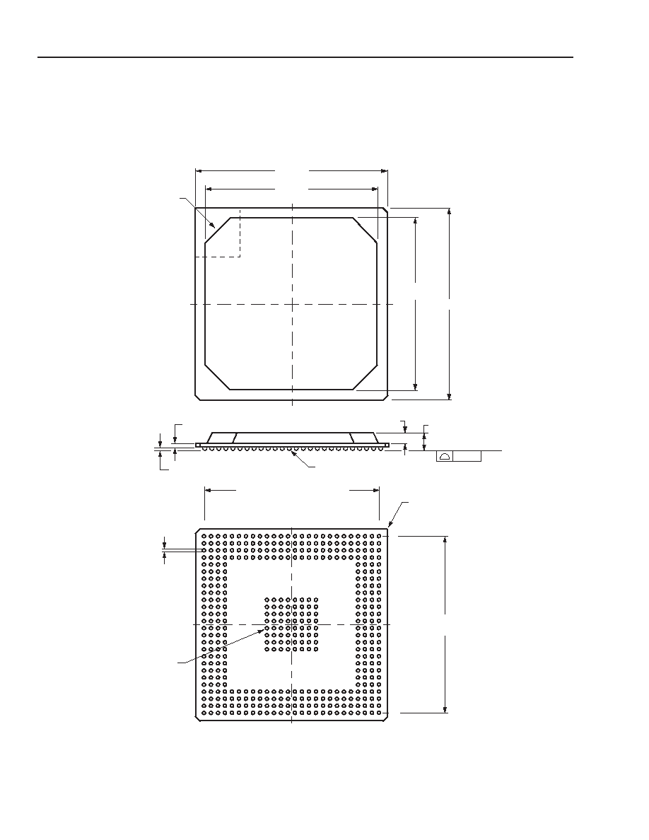
148
Lattice Semiconductor
Data Sheet
March, 2003
ORCA
Series 4 FPGAs
Package Outline Diagrams
(continued)
416-Pin PBGAM
Dimensions are in millimeters.
1139(F)
5-4409(F)
0.61 � 0.08
1.17 � 0.05
2.28 � 0.10
SEATING PLANE
SOLDER BALL
0.50 � 0.10
0.20
27.00
27.00
24.00
24.00
PIN A1
CORNER
AF
AE
AD
AC
AB
AA
Y
W
V
U
T
R
G
25 SPACES @ 1.00 = 25.00
P
N
M
L
K
J
H
1
2
3
4
5
6
7
8
9
10
12
14
16
18
22
24
26
20
11
13
15
17
21
19
23
25
F
E
D
C
B
A
CENTER ARRAY
FOR THERMAL
ENHANCEMENT
25 SPACES
@ 1.00 = 25.00
A1 BALL
CORNER
0.63 � 0.15
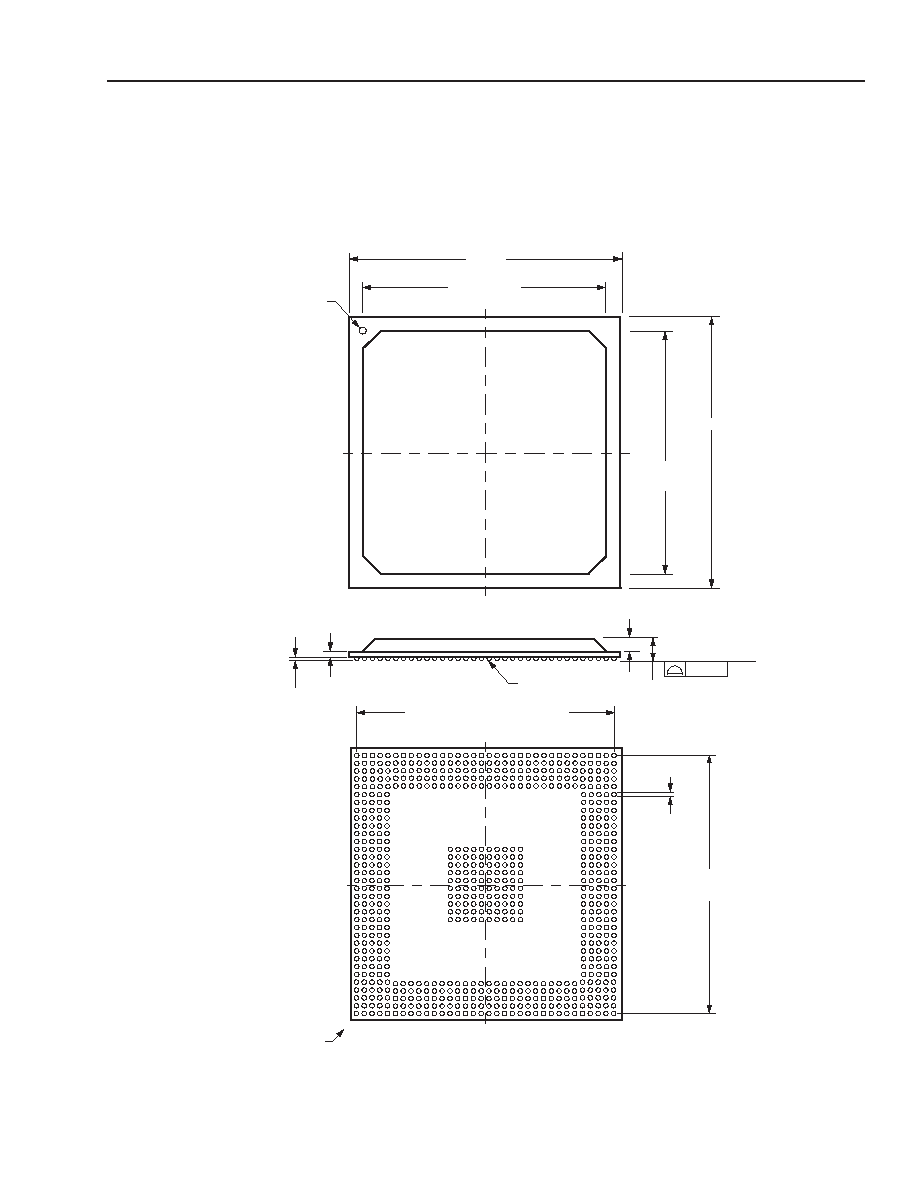
Lattice Semiconductor
149
Data Sheet
March, 2003
ORCA
Series 4 FPGAs
Package Outline Drawings
(continued)
680-Pin PBGAM
Dimensions are in millimeters.
5-4406(F)
SEATING PLANE
SOLDER BALL
0.50 � 0.10
0.20
35.00
T
D
H
AL
F
K
B
P
M
L
J
AH
R
C
E
Y
N
U
AN
G
AD
V
AM
AJ
AG
AE
AC
AA
W
AP
AK
AF
AB
A
19
30
26 28
24
32
22
20
18
4
6
8
10 12 14 16
2
34
5
23 25
7
31
29
15
21
3
27
11
17
9
13
1
33
33 SPACES @ 1.00 = 33.00
33 SPACES
A1 BALL
0.64 � 0.15
A1 BALL
@ 1.00 = 33.00
CORNER
30.00
1.170
+ 0.70
� 0.00
35.00
30.00
+ 0.70
� 0.00
IDENTIFIER ZONE
2.51 MAX
0.61 � 0.08

150
Lattice Semiconductor
Data Sheet
March, 2003
ORCA
Series 4 FPGAs
Ordering Information
Table 73. Device Type Options
Table 74. Recommended Temperature Range
Device
Voltage
OR4Exx
1.5 V internal
3.3 V/2.5 V/1.8 V/1.5 V I/O
Symbol
Description
Ambient Temperature
Junction Temperature
C
Commercial
0 �C to +70 �C
0 �C to +85 �C
I
Industrial
�40 �C to +85 �C
�40 �C to +100 �C
Device Family
OR4E02
OR4E04
OR4E06
OR4EXX
X
X
XX
XXX
Speed Grade
Package Type
BA = Plastic Ball Grid Array (PBGA)
BM = Fine-Pitch Plastic Ball Grid Array (PBGAM)
Ball Count
Grade
C = Commercial
I = Industrial

Lattice Semiconductor
151
Data Sheet
March, 2003
ORCA
Series 4 FPGAs
Table 75. Commercial Ordering Information
Note: For all but the slowest commercial speed grade, the speed grades on these devices are dual marked. For example, the commercial speed
grade -2XXXXXC is also marked with the industrial grade -1XXXXXI. The commercial grade is always one speed grade faster than the associ-
ated dual mark industrial grade. The slowest commercial speed grade is marked as commercial grade only.
Device Family
Part Number
Speed
Grade
Package
Type
Ball
Count
Grade
OR4E02
OR4E02-3BA352C
3
PBGA
352
C
OR4E02-3BM416C
3
PBGAM
416
C
OR4E02-3BM680C
3
PBGAM
680
C
OR4E02-2BA352C
2
PBGA
352
C
OR4E02-2BM416C
2
PBGAM
416
C
OR4E02-2BM680C
2
PBGAM
680
C
OR4E02-1BA352C
1
PBGA
352
C
OR4E02-1BM416C
1
PBGAM
416
C
OR4E02-1BM680C
1
PBGAM
680
C
OR4E04
OR4E04-3BA352C
3
PBGA
352
C
OR4E04-3BM416C
3
PBGAM
416
C
OR4E04-3BM680C
3
PBGAM
680
C
OR4E04-2BA352C
2
PBGA
352
C
OR4E04-2BM416C
2
PBGAM
416
C
OR4E04-2BM680C
2
PBGAM
680
C
OR4E04-1BA352C
1
PBGA
352
C
OR4E04-1BM416C
1
PBGAM
416
C
OR4E04-1BM680C
1
PBGAM
680
C
OR4E06
OR4E06-2BA352C
2
PBGA
352
C
OR4E06-2BM680C
2
PBGAM
680
C
OR4E06-1BA352C
1
PBGA
352
C
OR4E06-1BM680C
1
PBGAM
680
C

152
Lattice Semiconductor
Data Sheet
March, 2003
ORCA
Series 4 FPGAs
Table 76. Industrial Ordering Information
Note: For all but the slowest commercial speed grade, the speed grades on these devices are dual marked. For example, the commercial speed
grade -2XXXXXC is also marked with the industrial grade -1XXXXXI. The commercial grade is always one speed grade faster than the associ-
ated dual mark industrial grade. The slowest commercial speed grade is marked as commercial grade only.
Device Family
Part Number
Speed
Grade
Package
Type
Ball
Count
Grade
OR4E02
OR4E02-2BA352I
2
PBGA
352
I
OR4E02-2BM416I
2
PBGAM
416
I
OR4E02-2BM680I
2
PBGAM
680
I
OR4E02-1BA352I
1
PBGA
352
I
OR4E02-1BM416I
1
PBGAM
416
I
OR4E02-1BM680I
1
PBGAM
680
I
OR4E04
OR4E04-2BA352I
2
PBGA
352
I
OR4E04-2BM416I
2
PBGAM
416
I
OR4E04-2BM680I
2
PBGAM
680
I
OR4E04-1BA352I
1
PBGA
352
I
OR4E04-1BM416I
1
PBGAM
416
I
OR4E04-1BM680I
1
PBGAM
680
I
OR4E06
OR4E06-1BA352I
1
PBGA
352
I
OR4E06-1BM680I
1
PBGAM
680
I