
www.latticesemi.com
1
42g582g5_01
ORCA
Æ
ORT42G5 and ORT82G5
0.6 to 3.7 Gbits/s
XAUI and FC FPSCs
March 2003
Data Sheet
© 2003 Lattice Semiconductor Corp. All Lattice trademarks, registered trademarks, patents, and disclaimers are as listed at www.latticesemi.com/legal. All other brand
or product names are trademarks or registered trademarks of their respective holders. The specifications and information herein are subject to change without notice.
Introduction
Lattice Semiconductor has developed a family of next generation FPSCs intended for high-speed serial backplane
data transmission. Built on the Series 4 reconfigurable embedded System-on-a-Chip (SoC) architecture, the
ORT42G5 and ORT82G5 are made up of SERDES transceivers containing four and eight channels respectively,
each operating at up to 3.7 Gbits/s, with a full-duplex synchronous interface with built-in Rx Clock and Data Recov-
ery (CDR), and transmitter preemphasis, along with more than 400K usable FPGA system gates. The CDR cir-
cuitry available from Lattice's high-speed I/O portfolio (sysHSITM), has already been proven in numerous
applications, to create interfaces for SONET/SDH, Fibre Channel, and Ethernet (GbE, 10 GbE) applications.
Designers can also use these devices to drive high-speed data transfer across buses within any generic system.
For example, designers can build a bridge for 10 G Ethernet: the high-speed SERDES interfaces can comprise a
XAUI interface with a configurable back-end interface such as XGMII. The ORT42G5 and ORT82G5 can also be
used to provide a full 10 G backplane data connection and, in the case of the ORT82G5, provide both work and
protection links between a line card and switch fabric.
The ORT42G5 and ORT82G5 provide a clockless high-speed interface for interdevice communication on a board
or across a backplane. The built-in clock recovery of the ORT42G5 and ORT82G5 allows for higher system perfor-
mance, easier-to-design clock domains in a multiboard system, and fewer signals on the backplane. Network
designers will benefit from the backplane transceiver as a network termination device. The device supports embed-
ded 8b/10b encoding/decoding and link state machines for 10 G Ethernet, and Fibre Channel.
The ORT82G5 is pinout compatible with a sister device, the ORSO82G5, which implements eight channels of
SERDES with SONET scrambling and cell processing. The ORT42G5 is pin compatible with the ORSO42G5,
which implements four channels of SERDES with SONET scrambling and cell processing.
Table 1. ORCA ORT42G5 and ORT82G5 Family ≠ Available FPGA Logic
Note: ORCA ORT42G5 information is preliminary.
Device
PFU Rows
PFU
Columns
Total PFUs
FPGA Max.
User I/O
LUTs
EBR
Blocks
2
EBR Bits
2
(K)
FPGA System
Gates (K)
1
ORT42G5
36
36
1296
204
10,368
12
111
333-643
ORT82G5
36
36
1296
372
10,368
12
111
333-643
1. The embedded core, Embedded System Bus, FPGA interface and MPI are not included in the above gate counts. The system gate ranges
are derived from the following: Minimum System Gates assumes 100% of the PFUs are used for logic only (No PFU RAM) with 40% EBR
usage and two PLLs. Maximum System Gates assumes 80% of the PFUs are for logic, 20% are used for PFU RAM, with 80% EBR usage
and four PLLs.
2. There are two 4K x 36 (144K bits each) RAM blocks in the embedded core which are also accessible by the FPGA logic.

Lattice Semiconductor
ORCA ORT42G5 and ORT82G5 Data Sheet
2
Table of Contents
Introduction .................................................................. 1
Table of Contents......................................................... 2
Embedded Function Features...................................... 4
Programmable Features .............................................. 5
Programmable Logic System Features........................ 6
Description ................................................................... 7
What is an FPSC?........................................... 7
FPSC Overview............................................... 7
FPSC Gate Counting ...................................... 7
FPGA/Embedded Core Interface .................... 7
FPSC Design Kit ............................................. 7
FPGA Logic Overview..................................... 8
PLC Logic........................................................ 8
Programmable I/O........................................... 8
Routing............................................................ 9
System-Level Features ................................................ 9
Microprocessor Interface................................. 9
System Bus ................................................... 10
Phase-Locked Loops .................................... 10
Embedded Block RAM .................................. 10
Configuration................................................. 10
Additional Information ................................... 11
ORT42G5/ORT82G5 Overview ................................. 11
Embedded Core Overview ............................ 11
Serializer and Deserializer (SERDES) .......... 11
MUX/DEMUX Block ...................................... 12
Multi-channel Alignment FIFOs..................... 12
XAUI and Fibre Channel Link State
Machines ................................................ 12
FPGA/Embedded Core Interface .................. 12
Dual Port RAMs ............................................ 13
FPSC Configuration ...................................... 13
Backplane Transceiver Core Detailed Description .... 13
8b/10b Encoding and Decoding .................... 14
Transmit Path (FPGA to Backplane) Logic ... 16
8b/10b Encoder and 1:10 Multiplexer ........... 18
CML Output Buffer ........................................ 18
Receive Path (Backplane to FPGA) Logic .... 19
Link State Machines...................................... 24
XAUI Link Synchronization Function............. 25
Multi-channel Alignment............................................. 27
ORT42G5 Multi-channel Alignment .............. 27
ORT82G5 Multi-channel Alignment .............. 28
XAUI Lane Alignment Function (Lane
Deskew).................................................. 29
Mixing Half-rate, Full-rate Modes .................. 30
Multi-channel Alignment Configuration ...................... 30
ORT42G5 Configuration ............................... 30
ORT82G5 Configuration ............................... 31
ORT42G5 Alignment Sequence.................... 32
ORT82G5 Alignment Sequence.................... 33
Reference Clocks and Internal Clock Distribution...... 37
Reference Clock Requirements .................... 37
Synthesized and Recovered Clocks ............. 37
Internal Clock Signals at the FPGA/Core Interface
for the ORT42G5 ................................................. 38
Transmit and Receive Clock Rates............... 39
Transmit Clock Source Selection .................. 39
Recommended Transmit Clock Distribution
for the ORT42G5 .................................... 39
Multi-Channel Alignment Clocking
Strategies for the ORT42G5 ................... 41
Internal Clock Signals at the FPGA/Core Interface
for the ORT82G5 ................................................. 43
Transmit and Receive Clock Rates............... 44
Transmit Clock Source Selection .................. 44
Recommended Transmit Clock Distribution
for the ORT82G5 .................................... 45
Multi-Channel Alignment Clocking
Strategies for the ORT82G5 ................... 47
Reset Operation ......................................................... 49
Start Up Sequence for the ORT42G5 ........... 50
Start Up Sequence for the ORT82G5 ........... 51
Test Modes ................................................................ 51
Loopback Testing.......................................... 51
High-Speed Serial Loopback at the CML Buffer
Interface.................................................. 52
Parallel Loopback at the SERDES
Boundary ................................................ 53
Parallel Loopback at MUX/DEMUX
Boundary, Excluding SERDES ............... 54
SERDES Characterization Test Mode .......... 55
Embedded Core Block RAM ......................... 56
Memory Maps ............................................................ 58
Definition of Register Types .......................... 58
ORT42G5 Memory Map................................ 58
ORT82G5 Memory Map................................ 67
Recommended Board-level Clocking for
the ORT42G5 and ORT82G5 ................. 73
Absolute Maximum Ratings ....................................... 75
Recommended Operating Conditions ........................ 75
SERDES Electrical and Timing Characteristics ......... 75
High Speed Data Transmitter........................ 76
High Speed Data Receiver............................ 77
External Reference Clock ............................. 79
Embedded Core Timing Characteristics ....... 79
Pin Descriptions ......................................................... 80
Power Supplies for ORT42G5 AND ORT82G5.......... 84
Power Supply Descriptions ........................... 84
Recommended Power Supply
Connections............................................ 85
Recommended Power Supply Filtering
Scheme................................................... 85
Package Information .................................................. 87
Package Pinouts ........................................... 87
Package Thermal Characteristics Summary 114

Lattice Semiconductor
ORCA ORT42G5 and ORT82G5 Data Sheet
3
JA ............................................................. 114
JC............................................................. 115
JC ............................................................. 115
JB ............................................................. 115
FPSC Maximum Junction Temperature ...... 115
Package Thermal Characteristics ............... 115
Heat Sink Vendors for BGA Packages........ 116
Package Parasitics...................................... 116
Package Outline Drawings.......................... 117
Ordering Information ................................................ 118

Lattice Semiconductor
ORCA ORT42G5 and ORT82G5 Data Sheet
4
Embedded Function Features
∑ High-speed SERDES with programmable serial data rates over the range 0.6-3.7 Gbits/s. Operation has been
demonstrated on design tolerance devices at 3.7 Gbits/s across 26 in. of FR-4 backplane and at 3.125 Gbits/s
across 40 in. of FR-4 backplane across temperature and voltage specifications.
∑ Asynchronous operation per receive channel with the receiver frequency tolerance based on one reference clock
per block channels (separate PLL per channel).
∑ Ability to select full-rate or half-rate operation per transmit or receive channel by setting the appropriate control
registers.
∑ Programmable one-half amplitude transmit mode for reduced power in chip-to-chip application.
∑ Transmit preemphasis (programmable) for improved receive data eye opening.
∑ 32-bit (8b/10b) or 40-bit (raw data) parallel internal bus for data processing in FPGA logic.
∑ Provides a 10 Gbits/s backplane interface to switch fabric. Also supports multiple port cards at 2.5 Gbits/s.
∑ 3.125 Gbits/s SERDES compliant with XAUI serial data specification for 10 G Ethernet applications with protec-
tion.
∑ IEEE 802.3ae compliant XAUI transceiver. Includes embedded XAUI link state machine.
∑ Compliant to FC-0 specification for 1 Gbps, 2Gbps, 10 Gbps (FC-XAUI) modes. Includes Fibre Channel link state
machine.
∑ High-Speed Interface (HSI) function for clock/data recovery serial backplane data transfer without external
clocks.
∑ SERDES has low-power CML buffers. Support for 1.5 V/1.8 V I/Os. Allows use with optical transceiver, coaxial
copper media, shielded twisted pair wiring or high-speed backplanes such as FR-4.
∑ Power down option of SERDES HSI receiver or transmitter on a per-channel basis.
∑ Automatic lock to reference clock in the absence of valid receive data.
∑ High-speed and low-speed loopback test modes.
∑ Requires no external component for clock recovery and frequency synthesis.
∑ SERDES characterization pins available to control/monitor the internal interface to one SERDES block.
∑ SERDES HSI automatically recovers from loss-of-clock once its reference clock returns to normal operating
state.
∑ Built-in boundary scan (IEEE
Æ
1149.1 and 1149.2 JTAG) for the programmable I/Os, not including the SERDES
interface.
∑ FIFOs can align incoming data either across all eight channels (ORT82G5 only), across one or two groups of
four channels, or across two or four groups of two channels. Alignment is done either using comma characters or
by using the /A/ character in XAUI mode. Optionally, the alignment FIFOs can be bypassed for asynchronous
operation between channels. (Each channel includes its own clock and frame pulse or comma detect.)
∑ Addition of two 4K x 36 dual-port RAMs with access to the programmable logic.
∑ The ORT82G5 is pinout compatible to the ORCA ORSO82G5 SONET backplane driver FPSC. The ORT42G5 is
pin compatible to the ORSO42G5.

Lattice Semiconductor
ORCA ORT42G5 and ORT82G5 Data Sheet
5
Programmable Features
∑ High-performance programmable logic:
≠ 0.16 µm 7-level metal technology.
≠ Internal performance of >250 MHz.
≠ Over 400K usable system gates.
≠ Meets multiple I/O interface standards.
≠ 1.5 V operation (30% less power than 1.8V operation) translates to greater performance.
∑ Traditional I/O selections:
≠ LVTTL (3.3V) and LVCMOS (2.5 V and 1.8 V) I/Os.
≠ Per pin-selectable I/O clamping diodes provide 3.3V PCI compliance.
≠ Individually programmable drive capability: 24 mA sink/12 mA source, 12 mA sink/6 mA source, or 6 mA
sink/3 mA source.
≠ Two slew rates supported (fast and slew-limited).
≠ Fast-capture input latch and input Flip-Flop (FF)/latch for reduced input setup time and zero hold time.
≠ Fast open-drain drive capability.
≠ Capability to register 3-state enable signal.
≠ Off-chip clock drive capability.
≠ Two-input function generator in output path.
∑ New programmable high-speed I/O:
≠ Single-ended: GTL, GTL+, PECL, SSTL3/2 (class I and II), HSTL (Class I, III, IV), ZBT, and DDR.
≠ Double-ended: LVDS, bused-LVDS, and LVPECL. Programmable (on/off) internal parallel termination (100
) is also supported for these I/Os.
∑ New
capability to (de)multiplex I/O signals:
≠ New DDR on both input and output at rates up to 350 MHz (700 MHz effective rate).
≠ New 2x and 4x downlink and uplink capability per I/O (i.e., 50 MHz internal to 200 MHz I/O).
∑ Enhanced twin-block Programmable Function Unit (PFU):
≠ Eight 16-bit Look-Up Tables (LUTs) per PFU.
≠ Nine user registers per PFU, one following each LUT, and organized to allow two nibbles to act indepen-
dently, plus one extra for arithmetic operations.
≠ New register control in each PFU has two independent programmable clocks, clock enables, local
SET/RESET, and data selects.
≠ New LUT structure allows flexible combinations of LUT4, LUT5, new LUT6, 4
1 MUX, new 8
1 MUX,
and ripple mode arithmetic functions in the same PFU.
≠ 32 x 4 RAM per PFU, configurable as single- or dual-port. Create large, fast RAM/ROM blocks (128 x 8 in
only eight PFUs) using the Supplemental Logic and Interconnect Cell (SLIC) decoders as bank drivers.
≠ Soft-Wired LUTs (SWL) allow fast cascading of up to three levels of LUT logic in a single PFU through fast
internal routing which reduces routing congestion and improves speed.
≠ Flexible fast access to PFU inputs from routing.
≠ Fast-carry logic and routing to all four adjacent PFUs for nibble-wide, byte-wide, or longer arithmetic func-
tions, with the option to register the PFU carry-out.
∑ Abundant high-speed buffered and nonbuffered routing resources provide 2x average speed improvements over
previous architectures.
∑ Hierarchical routing optimized for both local and global routing with dedicated routing resources. This results in
faster routing times with predictable and efficient performance.
∑ SLIC provides eight 3-statable buffers, up to a 10-bit decoder, and PAL
Æ
-like AND-OR-Invert (AOI) in each pro-
grammable logic cell.
∑ New 200 MHz embedded block-port RAM blocks, two read ports, two write ports, and two sets of byte lane
enables. Each embedded RAM block can be configured as:

Lattice Semiconductor
ORCA ORT42G5 and ORT82G5 Data Sheet
6
≠ 1--512 x 18 (block-port, two read/two write) with optional built in arbitration.
≠ 1--256 x 36 (dual-port, one read/one write).
≠ 1--1K x 9 (dual-port, one read/one write).
≠ 2--512 x 9 (dual-port, one read/one write for each).
≠ 2 RAMS with arbitrary number of words whose sum is 512 or less by 18 (dual-port, one read/one write).
≠ Supports joining of RAM blocks.
≠ Two 16 x 8-bit content addressable memory (CAM) support.
≠ FIFO 512 x 18, 256 x 36, 1K x 9, or dual 512 x 9.
≠ Constant multiply (8 x 16 or 16 x 8).
≠ Dual variable multiply (8 x 8).
∑ Embedded 32-bit internal system bus plus 4-bit parity interconnects FPGA logic, microprocessor interface (MPI),
embedded RAM blocks, and embedded standard cell blocks with 100 MHz bus performance. Included are built-
in system registers that act as the control and status center for the device.
∑ Built-in testability:
≠ Full boundary scan (IEEE 1149.1 and Draft 1149.2 JTAG).
≠ Programming and readback through boundary scan port compliant to IEEE Draft 1532:D1.7.
≠ TS_ALL testability function to 3-state all I/O pins.
≠ New temperature-sensing diode.
∑ Improved built-in clock management with Programmable Phase-Locked Loops (PPLLs) provide optimum clock
modification and conditioning for phase, frequency, and duty cycle from 20 MHz up to 420 MHz. Multiplication of
the input frequency up to 64x and division of the input frequency down to 1/64x possible.
∑ New cycle stealing capability allows a typical 15% to 40% internal speed improvement after final place and route.
This feature also enables compliance with many setup/hold and clock to out I/O specifications and may provide
reduced ground bounce for output buses by allowing flexible delays of switching output buffers.
∑ Per channel Pseudo-Random Bit Sequence (PRBS) generator and checker in FPGA logic.
Programmable Logic System Features
∑ PCI local bus compliant for FPGA I/Os.
∑ Improved
PowerPC
Æ
860 and PowerPC II high-speed synchronous microprocessor interface can be used for
configuration, readback, device control, and device status, as well as for a general-purpose interface to the
FPGA logic, RAMs, and embedded standard cell blocks. Glueless interface to synchronous PowerPC processors
with user-configurable address space provided.
∑ New embedded
system bus facilitates communication among the microprocessor interface, configuration logic,
Embedded Block RAM, FPGA logic, and embedded standard cell blocks.
∑ Variable size bused readback of configuration data capability with the built-in microprocessor interface and sys-
tem bus.
∑ Internal, 3-state, and bidirectional buses with simple control provided by the SLIC.
∑ New clock routing structures for global and local clocking significantly increases speed and reduces skew (<200
ps for OR4E04).
∑ New local clock routing structures allow creation of localized clock trees.
∑ Two new edge clock routing structures allow up to six high-speed clocks on each edge of the device for improved
setup/hold and clock to out performance.
∑ New Double-Data Rate (DDR) and Zero-Bus Turn-around (ZBT) memory interfaces support the latest high-
speed memory interfaces.
∑ New 2x/4x uplink and downlink I/O capabilities interface high-speed external I/Os to reduced speed internal
logic.

Lattice Semiconductor
ORCA ORT42G5 and ORT82G5 Data Sheet
7
Description
What is an FPSC?
FPSCs, or field-programmable system chips, are devices that combine field-programmable logic with ASIC or
mask-programmed logic on a single device. FPSCs provide the time to market and the flexibility of FPGAs, the
design effort savings of using soft Intellectual Property (IP) cores, and the speed, design density, and economy of
ASICs.
FPSC Overview
Lattice's Series 4 FPSCs are created from Series 4 ORCA FPGAs. To create a Series 4 FPSC, several columns of
Programmable Logic Cells (see FPGA Logic Overview section for FPGA logic details) are added to an embedded
logic core. Other than replacing some FPGA gates with ASIC gates, at greater than 10:1 efficiency, none of the
FPGA functionality is changed--all of the Series 4 FPGA capability is retained including: the Embedded Block
RAMs, MicroProcessor Interface (MPI), boundary scan, etc. The columns of programmable logic are replaced at
the right of the device, allowing pins from the replaced columns to be used as I/O pins for the embedded core. The
remainder of the device pins retain their FPGA functionality.
FPSC Gate Counting
The total gate count for an FPSC is the sum of its embedded core (standard-cell/ASIC gates) and its FPGA gates.
Because FPGA gates are generally expressed as a usable range with a nominal value, the total FPSC gate count
is sometimes expressed in the same manner. Standard-cell ASIC gates are, however, 10 to 25 times more silicon-
area efficient than FPGA gates. Therefore, an FPSC with an embedded function is gate equivalent to an FPGA with
a much larger gate count.
FPGA/Embedded Core Interface
The interface between the FPGA logic and the embedded core has been enhanced to allow for a greater number of
interface signals than on previous FPSC architectures. Compared to bringing embedded core signals off-chip, this
on-chip interface is much faster and requires less power. All of the delays for the interface are precharacterized and
accounted for in the Lattice ispLEVERTM System software.
Series 4 based FPSCs expand this interface by providing a link between the embedded block and the multi-master
32-bit system bus in the FPGA logic. This system bus allows the core easy access to many of the FPGA logic func-
tions including the Embedded Block RAMs and the microprocessor interface.
Clock spines also can pass across the FPGA/embedded core boundary. This allows for fast, low-skew clocking
between the FPGA and the embedded core. Many of the special signals from the FPGA, such as DONE and global
set/reset, are also available to the embedded core, making it possible to fully integrate the embedded core with the
FPGA as a system.
For even greater system flexibility, FPGA configuration RAMs are available for use by the embedded core. This
allows for user-programmable options in the embedded core, in turn allowing for greater flexibility. Multiple embed-
ded core configurations may be designed into a single device with user-programmable control over which configu-
rations are implemented, as well as the capability to change core functionality simply by reconfiguring the device.
FPSC Design Kit
Development is facilitated by an FPSC design kit which, together with ispLEVER System software and third-party
synthesis and simulation engines, provides all software and documentation required to design and verify an FPSC
implementation. Included in the kit are the FPSC configuration manager, Synopsys Smart Model
Æ
, and/or complied
Verilog simulation model, HSPICE and/or IBIS models for I/O buffers, and complete online documentation. The kit's
software coupled with the
design environment, provides a seamless FPSC design environment. More information
can be obtained by visiting the Lattice
web site or contacting a local sales office, both listed on the last page of this
document.

Lattice Semiconductor
ORCA ORT42G5 and ORT82G5 Data Sheet
8
FPGA Logic Overview
The ORCA Series 4 architecture is a new generation of SRAM-based programmable devices from Lattice. It
includes enhancements and innovations geared toward today's high-speed systems on a single chip. Designed
with networking applications in mind, the Series 4 family incorporates system-level features that can further reduce
logic requirements and increase system speed. ORCA Series 4 devices contain many new patented enhance-
ments and are offered in a variety of packages and speed grades.
The hierarchical architecture of the logic, clocks, routing, RAM, and system-level blocks create a seamless merge
of FPGA and ASIC designs. Modular hardware and software technologies enable System-on-Chip integration with
true plug-and-play design implementation.
The architecture consists of four basic elements: Programmable Logic Cells (PLCs), Programmable I/O cells
(PIOs), Embedded Block RAMs (EBRs), plus supporting system-level features. These elements are interconnected
with a rich routing fabric of both global and local wires. An array of PLCs is surrounded by common interface blocks
which provide an abundant interface to the adjacent PLCs or system blocks. Routing congestion around these crit-
ical blocks is eliminated by the use of the same routing fabric implemented within the programmable logic core.
Each PLC contains a PFU, SLIC, local routing resources, and configuration RAM. Most of the FPGA logic is per-
formed in the PFU, but decoders, PAL-like functions, and 3-state buffering can be performed in the SLIC. The PIOs
provide device inputs and outputs and can be used to register signals and to perform input demultiplexing, output
multiplexing, uplink and downlink functions, and other functions on two output signals.
Large blocks of 512 x 18 block-port RAM complement the existing distributed PFU memory. The RAM blocks can
be used to implement RAM, ROM, FIFO, multiplier, and CAM. Some of the other system-level functions include the
MPI, PLLs, and the Embedded System Bus (ESB).
PLC Logic
Each PFU within a PLC contains eight 4-input (16-bit) LUTs, eight latches/FFs, and one additional Flip-Flop that
may be used independently or with arithmetic functions.
The PFU is organized in a twin-block fashion; two sets of four LUTs and FFs that can be controlled independently.
Each PFU has two independent programmable clocks, clock enables, local set/reset, and data selects. LUTs may
also be combined for use in arithmetic functions using fast-carry chain logic in either 4-bit or 8-bit modes. The
carry-out of either mode may be registered in the ninth FF for pipelining.
Each PFU may also be configured as a synchronous 32 x 4 single- or dual-port RAM or ROM. The FFs (or latches)
may obtain input from LUT outputs or directly from invertible PFU inputs, or they can be tied high or tied low. The
FFs also have programmable clock polarity, clock enables, and local set/reset.
The SLIC is connected from PLC routing resources and from the outputs of the PFU. It contains eight 3-state, bidi-
rectional buffers, and logic to perform up to a 10-bit AND function for decoding, or an AND-OR with optional
INVERT to perform PAL-like functions. The 3-state drivers in the SLIC and their direct connections from the PFU
outputs make fast, true, 3-state buses possible within the FPGA, reducing required routing and allowing for real-
world system performance.
Programmable I/O
The Series 4 PIO addresses the demand for the flexibility to select I/Os that meet system interface requirements.
I/Os can be programmed in the same manner as in previous ORCA devices, with the additional new features which
allow the user the flexibility to select new I/O types that support High-Speed Interfaces.
Each PIO contains four programmable I/O pads and is interfaced through a common interface block to the FPGA
array. The PIO is split into two pairs of I/O pads with each pair having independent clock enables, local set/reset,
and global set/reset. On the input side, each PIO contains a programmable latch/Flip-Flop which enables very fast
latching of data from any pad. The combination provides for very low setup requirements and zero hold times for

Lattice Semiconductor
ORCA ORT42G5 and ORT82G5 Data Sheet
9
signals coming on-chip. It may also be used to demultiplex an input signal, such as a multiplexed address/data sig-
nal, and register the signals without explicitly building a demultiplexer with a PFU.
On the output side of each PIO, an output from the PLC array can be routed to each output Flip-Flop, and logic can
be associated with each I/O pad. The output logic associated with each pad allows for multiplexing of output signals
and other functions of two output signals.
The output FF, in combination with output signal multiplexing, is particularly useful for registering address signals to
be multiplexed with data, allowing a full clock cycle for the data to propagate to the output. The output buffer signal
can be inverted, and the 3-state control can be made active-high, active-low, or always enabled. In addition, this 3-
state signal can be registered or nonregistered.
The Series 4 I/O logic has been enhanced to include modes for speed uplink and downlink capabilities. These
modes are supported through shift register logic, which divides down incoming data rates or multiplies up outgoing
data rates. This new logic block also supports high-speed DDR mode requirements where data is clocked into and
out of the I/O buffers on both edges of the clock.
The new programmable I/O cell allows designers to select I/Os which meet many new communication standards
permitting the device to hook up directly without any external interface translation. They support traditional FPGA
standards as well as high-speed, single-ended, and differential-pair signaling. Based on a programmable, bank-ori-
ented I/O ring architecture, designs can be implemented using 3.3V, 2.5V, 1.8V, and 1.5V referenced output levels.
Routing
The abundant routing resources of the Series 4 architecture are organized to route signals individually or as buses
with related control signals. Both local and global signals utilize high-speed buffered and nonbuffered routes. One
PLC segmented (x1), six PLC segmented (x6), and bused half chip (xHL) routes are patterned together to provide
high connectivity with fast software routing times and high-speed system performance.
Eight fully distributed primary clocks are routed on a low-skew, high-speed distribution network and may be
sourced from dedicated I/O pads, PLLs, or the PLC logic. Secondary and edge-clock routing is available for fast
regional clock or control signal routing for both internal regions and on device edges. Secondary clock routing can
be sourced from any I/O pin, PLLs, or the PLC logic.
The improved routing resources offer great flexibility in moving signals to and from the logic core. This flexibility
translates into an improved capability to route designs at the required speeds when the I/O signals have been
locked to specific pins.
System-Level Features
The Series 4 also provides system-level functionality by means of its microprocessor interface, Embedded System
Bus, block-port Embedded Block RAMs, universal programmable Phase-Locked Loops, and the addition of highly
tuned networking specific Phase-locked Loops. These functional blocks allow for easy glueless system interfacing
and the capability to adjust to varying conditions in today's high-speed networking systems.
Microprocessor Interface
The MPI provides a glueless interface between the FPGA and PowerPC microprocessors. Programmable in 8-, 16,
and 32-bit interfaces with optional parity to the Motorola
Æ
PowerPC 860 bus, it can be used for configuration and
readback, as well as for FPGA control and monitoring of FPGA status. All MPI transactions utilize the Series 4
Embedded System Bus at 66 MHz performance.
A system-level microprocessor interface to the FPGA user-defined logic following configuration, through the system
bus, including access to the Embedded Block RAM and general user-logic, is provided by the MPI. The MPI sup-
ports burst data read and write transfers, allowing short, uneven transmission of data through the interface by
including data FIFOs. Transfer accesses can be single beat (1 x 4 bytes or less), 4-beat (4 x 4 bytes), 8-beat (8 x 2
bytes), or 16-beat (16 x 1 bytes).

Lattice Semiconductor
ORCA ORT42G5 and ORT82G5 Data Sheet
10
System Bus
An on-chip, multimaster, 8-bit system bus with 1-bit parity facilitates communication among the MPI, configuration
logic, FPGA control, status registers, Embedded Block RAMs, as well as user logic. Utilizing the AMBA specifica-
tion Rev 2.0 AHB protocol, the Embedded System Bus offers arbiter, decoder, master, and slave elements. Master
and slave elements are also available for the user-logic and a slave interface is used for control and status of the
embedded backplane transceiver portion of the device.
The system bus control registers can provide control to the FPGA such as signaling for reprogramming, reset func-
tions, and PLL programming. Status registers monitor INIT, DONE, and system bus errors. An interrupt controller is
integrated to provide up to eight possible interrupt resources. Bus clock generation can be sourced from the micro-
processor interface clock, configuration clock (for slave configuration modes), internal oscillator, user clock from
routing, or from the port clock (for JTAG configuration modes).
Phase-Locked Loops
Up to eight PLLs are provided on each Series 4 device, with four user PLLs generally provided for FPSCs. Pro-
grammable PLLs can be used to manipulate the frequency, phase, and duty cycle of a clock signal. Each PPLL is
capable of manipulating and conditioning clocks from 20 MHz to 200 MHz. Frequencies can be adjusted from 1/8x
to 8x, the input clock frequency. Each programmable PLL provides two outputs that have different multiplication fac-
tors but can have the same phase relationships. Duty cycles and phase delays can be adjusted in 12.5% of the
clock period increments. An automatic input buffer delay compensation mode is available for phase delay. Each
PPLL provides two outputs that can have programmable (12.5% steps) phase differences.
Embedded Block RAM
New 512 x 18 block-port RAM blocks are embedded in the FPGA core to significantly increase the amount of mem-
ory and complement the distributed PFU memories. The EBRs include two write ports, two read ports, and two
byte lane enables which provide four-port operation. Optional arbitration between the two write ports is available,
as well as direct connection to the high-speed system bus.
Additional logic has been incorporated to allow significant flexibility for FIFO, constant multiply, and two-variable
multiply functions. The user can configure FIFO blocks with flexible depths of 512K, 256K, and 1K including asyn-
chronous and synchronous modes and programmable status and error flags. Multiplier capabilities allow a multiple
of an 8-bit number with a 16-bit fixed coefficient or vice versa (24-bit output), or a multiple of two 8-bit numbers (16-
bit output). On-the-fly coefficient modifications are available through the second read/write port.
Two 16 x 8-bit CAMs per embedded block can be implemented in single match, multiple match, and clear modes.
The EBRs can also be preloaded at device configuration time.
Configuration
The FPGAs functionality is determined by internal configuration RAM. The FPGAs internal initialization/configura-
tion circuitry loads the configuration data at power up or under system control. The configuration data can reside
externally in an EEPROM or any other storage media. Serial EEPROMs provide a simple, low pin-count method for
configuring FPGAs.
The RAM is loaded by using one of several configuration modes. Supporting the traditional master/slave serial,
master/slave parallel, and asynchronous peripheral modes, the Series 4 also utilizes its microprocessor interface
and Embedded System Bus to perform both programming and readback. Daisy chaining of multiple devices and
partial reconfiguration are also permitted.
Other configuration options include the initialization of the embedded-block RAM memories and FPSC memory as
well as system bus options and bit stream error checking. Programming and readback through the JTAG (IEEE
1149.2) port is also available meeting In-System Programming (ISPTM) standards (IEEE 1532 Draft).

Lattice Semiconductor
ORCA ORT42G5 and ORT82G5 Data Sheet
11
Additional Information
Contact your local Lattice representative for additional information regarding the ORCA Series 4 FPGA devices, or
visit the Lattice web site at www.latticesemi.com.
ORT42G5/ORT82G5 Overview
The ORT42G5 and ORT82G5 FPSCs provide high-speed backplane transceivers combined with FPGA logic. They
are based on the 1.5V OR4E04 ORCA FPGA and have 36 x 36 arrays of Programmable Logic Cells (PLCs). The
embedded core, which contains the backplane transceivers is attached to the right side of the device and is inte-
grated directly into the FPGA array. A top level diagram of the basic chip configuration is shown in Figure 1.
Embedded Core Overview
The embedded core portions of the ORT42G5 and ORT82G5 contain respectively four or eight Clock and Data
Recovery (CDR) macrocells and Serialize/Deserialize (SERDES) blocks and support 8b/10b (
IEEE
802.3z)
encoded serial links. It is intended for high-speed serial backplane data transmission. Figure 1 shows the
ORT42G5 and ORT82G5 top level block diagram and the basic data flow. Boundary scan for the
ORT42G5/ORT82G5 only includes programmable I/Os and does not include any of the embedded block I/Os.
Figure 1. ORT42G5/ORT82G5 Top Level Block Diagram
The serial channels can each operate at up to 3.7 Gbits/s (2.96 Gbits/s data rate) with a full-duplex synchronous
interface with built-in clock recovery (CDR). The 8b/10b encoding provides guaranteed ones density for the CDR,
byte alignment, and error detection. The core is also capable of frame synchronization and physical link monitoring
and contains independent 4k x 36 RAM blocks. Overviews of the various blocks in the embedded core are pre-
sented in the following paragraphs.
Serializer and Deserializer (SERDES)
The SERDES portion of the core contains two transceiver blocks for serial data transmission at a selectable data
rate of 0.6-3.7 Gbits/s. Each SERDES channel features high-speed 8b/10b parallel I/O interfaces to other core
blocks and high-speed CML interfaces to the serial links.
The SERDES circuitry consists of receiver, transmitter, and auxiliary functional blocks. The receiver accepts high-
speed (up to 3.7 Gbits/s) serial data. Based on data transitions, the receiver locks an analog receive PLL for each
channel to retime the data, then demultiplexes the data down to parallel bytes and an accompanying clock.
The transmitter operates in the reverse direction. Parallel bytes are multiplexed up to 3.7 Gbits/s serial data for off-
chip communication. The transmitter generates the necessary 3.7 GHz clocks for operation from a lower speed ref-
erence clock.
SERDES w/
CLOCK/DATA
BYTE-
WIDE
DATA
8b/10b
DECODER/ENCODER
4 or 8 FULL-
0.6 Gbits/s
DATA
DUPLEX
SERIAL
CHANNELS
TO
3.7 Gbits/s
0.6 Gbits/s
DATA
TO
3.7 Gbits/s
CML
I/Os
ORCA
SERIES 4
FPGA LOGIC
STANDARD
FPGA I/Os
RECOVERY
4:1 MUX/1:4 DEMUX
AND MULTI-CHANNEL
ALIGNMENT FIFOs

Lattice Semiconductor
ORCA ORT42G5 and ORT82G5 Data Sheet
12
The transceivers are controlled and configured through the system bus in the FPGA logic and through the external
8-bit microprocessor interface of the FPGA. Each channel has associated dedicated registers that are readable
and writable. There are also global registers for control of common circuitry and functions.
The SERDES performs 8b/10b encoding and decoding for each channel. The 8b/10b transmission code can sup-
port either Ethernet or Fibre Channel specifications for serial encoding/decoding, special characters, and error
detection.
The user can disable the 8b/10b decoder to receive raw 10-bit words which will be rate reduced by the SERDES. If
this mode is chosen, the user must bypass the multi-channel alignment FIFOs.
The SERDES block contains its own dedicated PLLs for both transmit and receive clock generation. The user pro-
vides a reference clock of the appropriate frequency. The receiver PLLs extract the clock from the serial input data
and retime the data with the recovered clock.
MUX/DEMUX Block
The MUX/DEMUX block converts the data format for the high speed serial links to a wide, low-speed format for
crossing the CORE/FPGA interface. The intermediate interface to the SERDES macrocell runs at 1/10th the bit
rate of the data lane. The MUX/DEMUX converts the data rate and bus width so the interface to the FPGA core can
run at 1/4th this intermediate frequency, giving a range of 25.0-92.5 MHz for the data rates into and out of the
FPGA logic.
Multi-channel Alignment FIFOs
In the ORT82G5, the eight incoming data channels (four per SERDES block) can be independent of each other or
can be synchronized in several ways. Two channels within a SERDES block can be aligned together; channels A
and B and/or channels C and D. Alternatively, four channels in a SERDES block can be aligned together to form a
communication channel with a bandwidth of 10 Gbits/s. Finally, the alignment can be extended across both SER-
DES blocks to align all eight channels. Individual channels within an alignment group can be disabled (i.e., pow-
ered down) without disrupting other channels.
In the ORT42G5, the four incoming data channels (two per SERDES block) can be independent of each other or
can be synchronized in two ways. Two channels, channels C and D, within either SERDES block can be aligned
together. Alternatively, all four channels can be aligned together to form a communication channel with a bandwidth
of 10 Gbits/s. Individual channels within an alignment group can be disabled (i.e., powered down) without disrupt-
ing other channels.
XAUI and Fibre Channel Link State Machines
Two separate link state machines are included in the architecture. A XAUI compliant link state machine is included
in the embedded core to implement the IEEE 802.3ae standard. A separate state machine for Fibre Channel is
also implemented.
FPGA/Embedded Core Interface
In 8b/10b mode, the FPGA logic will receive/transmit 32-bits of data (up to 92.5 MHz) and 4 K_CTRL bits from/to
the embedded core. There are 8 data streams in each direction plus additional timing, status and control signals.
Data sent to the FPGA can be aligned using comma (/K/) characters or /A/ character as specified either by Fibre
Channel or by IEEE 802.3ae for XAUI based interfaces. The alignment character is made available to the FPGA
along with the data. The special characters K28.1, K28.5 and K28.7 are treated as valid comma characters by the
SERDES.
If the receive channel alignment FIFOs are bypassed, then each channel will provide its own receive clock in addi-
tion to data and comma character detect signals. If the 8b/10b decoders are bypassed, then 40-bit data streams
are passed to the FPGA logic. No channel alignment can be done in 8b/10b bypass mode.

Lattice Semiconductor
ORCA ORT42G5 and ORT82G5 Data Sheet
13
Dual Port RAMs
In addition to the backplane interface blocks, there are two independent memory blocks in the ASB. Each memory
block has a capacity of 4k words by 36 bits. It has one read port, one write port, and four byte-write-enable (active-
low) signals. The read data from the memory block is registered so that it works as a pipelined synchronous mem-
ory block.
FPSC Configuration
Configuration of the ORT42G5 and ORT82G5 occurs in two stages: FPGA bitstream configuration and embedded
core setup.
Prior to becoming operational, the FPGA goes through a sequence of states, including power up, initialization, con-
figuration, start-up, and operation. The FPGA logic is configured by standard FPGA bit stream configuration means
as discussed in the Series 4 FPGA data sheet.
After the FPGA configuration is complete, the options for the embedded core are set based on the contents of reg-
isters that are accessed through the FPGA system bus.
The system bus itself can be driven by an external PowerPC compliant microprocessor via the MPI block or via a
user master interface in FPGA logic. A simple IP block that drives the system by using the user register interface
and very little FPGA logic is available in the MPI/System Bus Technical Note. This IP block sets up the embedded
core via a state machine and allows the ORT42G5 and ORT82G5 to work in an independent system without an
external microprocessor interface.
Backplane Transceiver Core Detailed Description
The following sections describe the various logic blocks in the Embedded Core portion of the FPSC. The FPGA
section of the FPSC is identical to an ORCA OR4E04 FPGA except that the pads on one edge of the FPGA chip
are replaced by the Embedded Core. For a detailed description of the programmable logic functions, please see
the ORCA Series 4 FPGA Data Sheet and related application and technical notes.
The major functional blocks in the Embedded Core include:
∑ Two SERializer-DESerializer (SERDES) blocks and Clock and Data Recovery (CDR) circuitry
∑ 8b/10b encoder/decoders
∑ Transmit pre-emphasis circuitry
∑ 4-to-1 multiplexers (MUX) and 1-to-4 demultiplexers (DEMUX)
∑ Fibre channel synchronization state machine
∑ XAUI link alignment state machine
∑ Alignment FIFOs
∑ Embedded 4K x 36 RAM blocks (independent from transceiver logic).
A top level block diagram of the Embedded Core Logic is shown in Figure 2. The Embedded RAM blocks are not
shown. The external pins for the Embedded Core are listed later in this data sheet in Table 41 and the signals at the
Transceiver Embedded Core/FPGA interface for the ORT42G5 are listed in Table 8, Table 9 and Table 11; and for
the ORT82G5, in Table 8, Table and Table 12.

Lattice Semiconductor
ORCA ORT42G5 and ORT82G5 Data Sheet
14
Figure 2. Top Level Block Diagram, Embedded Core Logic (Channel AC)
The Embedded Core provides transceiver functionality for four or eight serial data channels and is organized into
two blocks, each supporting two or four channels. Each channel is identified by both a block identifier [A:B] and a
channel identifier [A:D]. In the ORT42G5 only the channel identifiers C and D are used. (This naming convention
follows that of the ORT82G5).
The data channels can operate independently or they can be combined together (aligned) to achieve higher bit
rates. The mode operation of the core is defined by a set of control registers, which can be written through the sys-
tem bus interface. Also, the status of the core is stored in a set of status registers, which can be read through the
system bus interface.
The transmitter section for each channel accepts 40 bits of data or 32 bits of data and eight control/status bits from
the FPGA logic and optionally encodes the data using 8b/10b encoding. It also accepts the low-speed reference
clock at the REFCLK input and uses this clock to synthesize the internal high-speed serial bit clock. The data is
then serialized and the serialized data are available at the differential CML output terminated in 86
to drive either
an optical transmitter or coaxial media or circuit board/backplane.
The receiver section receives high-speed serial data at its differential CML input port. These data are fed to the
clock recovery section which generates a recovered clock and retimes the data. The retimed data are also deseri-
alized and optionally 8b/10b decoded. The receiver also optionally recognizes the comma characters or code viola-
tions and aligns the bit stream to the proper word boundary. The resulting parallel data is optionally passed to the
multi-channel alignment block before it is presented to the FPGA logic.
8b/10b Encoding and Decoding
In 8b/10b mode, the FPGA logic will receive/transmit 32 bits of data and 4 K_CTRL bits from/to the embedded
core. In the transmit direction, four additional input bits force negative disparity coding. The embedded core logic
will encode the data to or decode the data from a 10-bit format according to the FC-PH ANSI X3.230:1994 stan-
dard (which is also the encoding used by the IEEE 802.3ae Ethernet standard). This encoding/decoding scheme
also allows for the transmission of special characters and supports error detection.
Common Logic, Block A
Next Channel
.
.
.
Last Channel (BD)
Backplane
Serial
Links
Receive Channel AC
2:1 MUX
(x40)
DEMUX
Block
Link State
Machine
RX SER-
DES Block
Multi -
Channel
Alignment
Block
TX SERDES
Block
Interface and
MUX Block
Transmit Channel AC
RCK78A
TCK78A
MRWDAC[39:0]
CV_SELAC
RWCKAC
RSYS_CLK_A2
TSYS_CLK_AC
TWDAC[31:0]
TCOMMAC[3:0]
.
.
.
FPGA
Logic
HDOUT[P:N]_AC
2
2
HDIN[P:N]_AC
REFCLK[P:N]_A
2

Lattice Semiconductor
ORCA ORT42G5 and ORT82G5 Data Sheet
15
Following the definitions and conventions used in defining the 8b/10b coding rules, each valid coded character has
a name corresponding to its 8-bit binary value:
∑ Dxx.y for data characters
∑ Kxx.y for special characters
∑ xx = the 5-bit input value, base 10, for bits ABCDE
∑ y = the 3-bit input value, base 10, for bits FGH
An 8b/10b encoder is designed to maintain a neutral average disparity. Disparity is the difference between the
number of 1s and 0s in the encoded word. Neutral disparity indicates the number of 1s and 0s are equal. Positive
disparity indicates more 1s than 0s. Negative disparity indicates more 0s than 1s. The average disparity deter-
mines the DC component of the signals on the serial line. Running disparity is a record of the cumulative disparity
of every encoded word, and is tracked by the encoder.
In order to maintain neutral disparity, two different codings are defined for each data value. The 8b/10b encoder in
the transmit path selects between (+) and (-) encoded word based on calculated disparity of the present data to
maintain neutral disparity
In the receive path, the clock and data recovery blocks retime the incoming data and 8b/10b decoders generate 8-
bit data based on the received 10-bit data. A sequence of valid 8b/10b coded characters has a maximum run
length of 5 bits (i.e., 5 consecutive ones or 5 consecutive zeros before a mandatory bit transition). This assures
adequate transitions for robust clock recovery.
The recovered data is aligned on a 10-bit boundaries by detecting and aligning to special characters in the incom-
ing data stream. Data is word aligned using the comma (/K/) character. A comma character is a special character
that contains a unique pattern (0011111 or its complement 1100000) in the 10-bit space that makes it useful for
delimiting word boundaries. The special characters K28.1, K28.5 and K28.7 contain this comma sequence and are
treated as valid comma characters by the SERDES.
The following table shows all of the valid special characters. All of the special characters are made available to the
FPGA logic; however only the comma characters are used by the SERDES logic. The different codings that are
possible for each data value are shown as encoded word (+) and encoded word (-). The table also illustrates the
8b/10b bit labeling convention. The bit positions of the 8-bit characters are labeled as H,G,F,E,D,C,B and A and the
bit positions of the 10-bit encoded characters are labeled as a, b, c, d, e, i, f, g, h, and j. The encoded words are
transmitted serially with bit `a' transmitted first and bit `j' transmitted last.
Table 2. Valid Special Characters
K Character
HGF EDCBA
765 43210
K Control
Encoded Word (≠)
Encoded Word (+)
abcdei fghj
abcdei fghj
K28.0
000 11100
1
001111 0100
110000 1011
K28.1 /comma/
001 11100
1
001111 1001
110000 0110
K28.2
010 11100
1
001111 0101
110000 1010
K28.3 /A/
011 11100
1
001111 0011
110000 1100
K28.4
100 11100
1
001111 0010
110000 1101
K28.5 /comma/
101 11100
1
001111 1010
110000 0101
K28.6
110 11100
1
001111 0110
110000 1001
K28.7 /comma/
111 11100
1
001111 1000
110000 0111
K23.7
111 10111
1
111010 1000
000101 0111
K27.7
111 11011
1
110110 1000
001001 0111
K29.7
111 11101
1
101110 1000
010001 0111
K30.7
111 11110
1
011110 1000
100001 0111

Lattice Semiconductor
ORCA ORT42G5 and ORT82G5 Data Sheet
16
Transmit Path (FPGA to Backplane) Logic
The transmitter section accepts four groups of either 8-bit unencoded data or 10-bit encoded data at the parallel
interface to the FPGA logic. It also uses the reference clock, REFCLK[P:N]_[A:B] to synthesize an internal high-
speed serial bit clock. The serialized transmitted data are available at the differential CML output pins to drive either
an optical transmitters, coaxial media or a circuit board backplane.
As shown in Figure 3, the basic blocks in the transmit path include:
Embedded Core/FPGA interface and 4:1 multiplexer
∑ Low speed parallel core/FPGA interface
∑ 4:1 multiplexer
Transmit SERDES
∑ 8b/10b Encoder
∑ 10:1 Multiplexer
∑ CML Output Buffer
Detailed descriptions of the logic blocks are given in following sections. Detailed descriptions of transmit clock dis-
tribution, including the transmit PLL are given in later sections of this data sheet.
Figure 3. Basic Logic Blocks, Transmit Path, Single Channel (Typical Reference Clock Frequency)
˜
4
FIFO
4:1 MUX
(x9)
PLL
CML
Buffer
with Pre-
emphasis
10:1
MUX
8B/10B
Encoder
(with
bypass)
Interface and MUX Block
TX SERDES Block
STBD_xx[7:0]
STBD_xx[8]
STBD_xx[9]
STBC311_xx
8
8-bit data
K-control
Force-ve disparity
312.5 MHz
HDOUTP_xx
HDOUTN_xx
REFCLKP_[A:B]
REFCLKN_[A:B]
CML
Buffer
Backplane
Serial
Link
FPGA
Logic
TWDxx[31:0]
32
TCOMMAxx[3:0]
4
TBIT9xx[3:0]
4
TSYS_CLK_xx
MUX
TCK78[A:B]
78.125 MHz
TCKSEL[0:1][A:B]
Logic Common to Block
From other channel
or channels
To other
channel or
channels
From Control
Register
{
{
For ORT42G5: xx = [AC, AD, BC or BD]
For ORT82G5: xx = [AA, AB, ... BD]
156.25 MHz
Lattice Semiconductor
ORCA ORT42G5 and ORT82G5 Data Sheet
17
Embedded Core/FPGA Logic Interface and 4:1 Multiplexer
These blocks provide the data formatting and transmit data and clock signal transfers between the Embedded Core
and the FPGA Logic. Control and status registers in the FPGA portion of the chip contain to control the transmit
logic and record status. These bits are passed to the core using the FPGA System Bus and are described in later
sections of this data sheet.
The low-speed transmit interface consists of a clock and 4 data bytes, each with an accompanying control bit. The
data bytes are conveyed to the MUX via the TWDxx[31:0] ports (where xx represents the channel label [AA,...,BD]
or [AC, AD, BC, BD]). The control bits are TCOMMAx[3:0] which define whether the input byte is to be interpreted
as data or as a special character and TBIT9xx[3:0] which are used to force negative disparity encoding. The data
and control signals are synchronized to the transmit clock, TSYS_CLK_xx. Both the data and control are strobed
into the core on the rising edge of TSYS_CLK_xx.
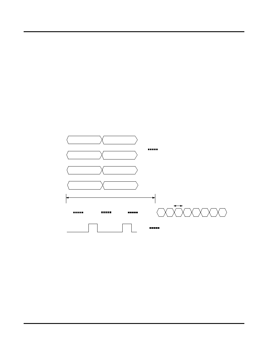
The MUX is responsible for taking 40 bits of data/control at the low-speed transmit interface and up-converting it to
10 bits of data/control at the SERDES transmit interface. The MUX has 2 clock domains - one based on the clock
received from the SERDES block and a second that comes from the FPGA at 1/4 the frequency of the SERDES
clock. The time sequence of interleaving data/control values is shown in Figure 4.
Figure 4. Transmit MUX Block Timing - Single Channel
SERDES Block
The SERDES block accepts either 8-bit data to be encoded or 10-bit unencoded data at the parallel input port from
the MUX/DEMUX block. It also accepts the reference clock at the REFCLK_[A:B] input and uses this clock to syn-
thesize the internal high-speed serial bit clock.
The internal STBC311xx clock is derived from the reference clock. The frequency of this clock depends on the set-
ting of the half-rate/full-rate control bit setting the mode of the SERDES and the frequency of the REFCLK_[A:B]
and/or that of the high-speed serial data. A falling edge on the STBC311xx clock port will cause a new data charac-
ter to be transferred into the SERDES block. The latency from the SERDES block input to the high-speed serial
output is 5 STBC311xx clock cycles, as shown in Figure 5.
p
q
r
s
t
x
y
z
STBDxx[9:0]
LATENCY = 4 TSYS_CLK_xx CLOCKS
TWDxx[31:24],
TSYS_CLK_xx
s
8
r
8
z
8
y
8
10-bit wide data
TWDxx[23:16],
TWDxx[15:8],
r
7-0,
y
7-0,
TCOMMAxx[3]
TCOMMAxx[2]
TCOMMAxx[1]
TCOMMAxx[0]
TWDxx[7:0],
s
7-0,
z
7-0,
TBIT9xx[0]
TBIT9xx[1]
TBIT9xx[2]
TBIT9xx[3]
q
9
r
9
s
9
z
9
y
9
x
9
p
7-0,
p
8
t
7-0,
q
8
t
8
x
8
q
7-0,
x
7-0,
p
9
t
9

Lattice Semiconductor
ORCA ORT42G5 and ORT82G5 Data Sheet
18
Figure 5. Transmit Path Timing - Single SERDES Channel
Each block also sends a clock to the FPGA logic. This clock, TCK78[A,B], is sourced from one of the four MUX
blocks and has the same frequency as TSYS_CLK_xx, but arbitrary phase. Within each MUX block, the low fre-
quency clock output is obtained by dividing by 4 the SERDES STBC311x clock which is used internally to synchro-
nize the transmit data words. TCKSEL control bits select the channel to source TCK78[A:B].
The internal signals STBDxx[9:0] (where xx is represents AA...BD or AC, AD, BC, BD) from the MUX block carry
unencoded character data and control bits. The 10th bit (STBDxx[9]) of each data lane into the SERDES is used to
force negative disparity encoding.
8b/10b Encoder and 1:10 Multiplexer
The 8b/10b encoder encodes the incoming 8-bit data into a 10-bit format as described previously. The input signals
to the block, STBDxx[7:0] are used for the 8-bit unencoded data. STBDxx[8] is used as the K_control input to indi-
cate whether the 8 data bits need to be encoded as special characters (K_control = 1) or as data characters
(K_control = 0). When STBDxx[9:0] = 1, negative disparity encoding is forced. When the encoder is bypassed STB-
Dxx[9:0] serve as the data bits for the 10-bit unencoded data.
Within the definition of the 8b/10b transmission code, the bit positions of the 10-bit encoded transmission charac-
ters are labeled as a, b, c, d, e, i, f, g, h, and j in that order. Bit a corresponds to STBDxx[0], bit b to STBDxx[1], bit
c to STBDxx[2], bit d to STBDxx[3], bit e to STBDxx[4], bit i to STBDxx[5], bit f to STBDxx[6], bit g to STBDxx[7], bit
h to STBDxx[8], and bit j to STBDxx[9].
The 10-bit wide parallel data is converted to serial data by the 10:1 Multiplexer. The serial data are then sent to the
CML output buffer and are transmitted serially with STBDxx[0] transmitted first and STBDxx[9] transmitted last.
CML Output Buffer
The transmitter's CML output buffer is terminated on-chip in 86 ohms to optimize the data eye as well as to reduce
the number of discrete components required. The differential output swing reaches a maximum of 1.2 V
PP
in the
normal amplitude mode. A half amplitude mode can be selected via configuration register bit HAMP_xx. Half ampli-
tude mode can be used to reduce power dissipation when the transmission medium has minimal attenuation or for
testing of the integrity (loss) of the physical medium.
A programmable preemphasis circuit is provided to boost the high frequencies in the transmit data signal to maxi-
mize the data eye opening at the far-end receiver. Preemphasis is particularly useful when the data are transmitted
over backplanes or low-quality coax cables which have a frequency-dependent amplitude loss. For example, for
FR4 material at 2.5 GHz, the attenuation compared to the 1.0 GHz value is about 3 dB. The attenuation is a result
of skin effect loss of the PCB conductor and the dielectric loss of the PCB substrate. This attenuation causes inter-
symbol interface which results in the closing of the data eye opening at the receiver.
.....
p
q
r
s
t
x
y
z
STBDxx[9:0]
.....
STBC311xx
.....
HDOUT_xx
p
4
p
5
p
6
p
7
p
8
p
9
p
0
p
1
p
2
p
3
LATENCY =
5 STBC311x CLOCKS

Lattice Semiconductor
ORCA ORT42G5 and ORT82G5 Data Sheet
19
Since this effect is predictable for a given type of PCB material, it is possible to compensate for this effect in two
ways - transmitter preemphasis and receiver equalization. Each of these techniques boosts the high frequency
components of the signal but transmit preemphasis is preferred due to the ease of implementation and the better
power utilization. It also gives a better signal-to-noise ratio because receiver equalization amplifies both the signal
and the noise at the receiver
Applying too much preemphasis when it is not required, for example when driving a short backplane path, will also
degrade the data eye opening at the receiver. In the ORT42G5 and ORT82G5 the degree of transmit preemphasis
can be programmed with a two-bit control from the microprocessor interface as shown in Table 3. The high-pass
transfer function of the preemphasis circuit is given by the following equation, where the value of a is shown in
Table 3.
H(z) = (1 ≠ az
≠1
)
(1)
Table 3. Preemphasis Settings
Receive Path (Backplane to FPGA) Logic
The receiver section receives high-speed serial data at the external differential CML input pins. These data are fed
to the clock recovery section which generates a recovered clock and retimes the data. Therefore the receive clocks
are asynchronous between channels. The retimed data are deserialized and presented as an 8-bit decoded or a
10-bit unencoded parallel data on the output port. The receiver also optionally recognizes comma characters,
detects code violations and aligns the bit stream to the proper word boundary.
As shown in Figure 6, the basic blocks in the receive path include:
Receive SERDES Block
∑ CML input buffer
∑ Receive PLL
∑ 1:10 demultiplexer (DEMUX)
∑ Clock and Data Recovery (CDR) section
∑ 10b/8b decoder
∑ 1:4 demultiplexer and Embedded Core/FPGA interface
∑ 1:4 DEMUX
∑ Low speed parallel Embedded Core/FPGA logic interface
∑ Multi-channel alignment logic
PE1
PE0
Amount of Preemphasis (a)
0
0
0% (No Preemphasis)
0
1
12.5%
1
0
12.5%
1
1
25%

Lattice Semiconductor
ORCA ORT42G5 and ORT82G5 Data Sheet
20
Figure 6. Basic Logic Blocks, Receive Path, Single Channel (Typical Reference Clock Frequency)
Each channel provides its own received clock, received data and K-character detect signals to the FPGA logic.
Incoming data from multiple channels can be aligned using comma (/K/) characters or /A/ character (as specified
either in Fibre Channel specifications or in IEEE
802.3ae for XAUI based interfaces). If the 8b/10b decoders are
bypassed, then 40-bit data streams are passed to the FPGA logic. No channel alignment can be done in this
8b/10b bypass mode.
Detailed descriptions of data synchronization, of the SERDES, DEMUX and Multi-Channel Alignment blocks and of
the Fibre Channel and XAUI state machines are given in following sections. Receive clock distribution is described
in a later section of this data sheet.
Synchronization
The SERDES RX logic performs four levels of synchronization on the incoming serial data stream. Each level
builds upon the previous, providing first bit, then byte (character), then channel (32-bit word), and finally multi-chan-
nel alignment. Each step is described functionally in the following paragraphs. The details of the logical implemen-
tations are described in subsequent sections.
Bit alignment
is the task of the Clock/Data Recovery (CDR) block. This block utilizes a PLL that locks to the transi-
tions in the incoming high-speed serial data stream, and outputs the extracted clock as well as the data. If the PLL
is unable to lock to the serial data stream, it instead locks to REFCLK[A:B] to stabilize the voltage-controlled oscil-
lator (VCO), and periodically switches back to the serial data stream to again attempt synchronization. This pro-
cess continues until a valid input data stream is detected and lock is achieved. The CDR can maintain lock on data
as long as the input data stream contains an adequate data "eye" (i.e., jitter is within specification) and the maxi-
mum data stream run length is not exceeded.
REFCLKP_[A:B]
REFCLKN_[A:B]
REFCLK
Buffer
MUX
RCK78[A:B]
78.125 MHz
RCKSEL[0:1][A:B]
Logic Common to Block
From other channel
or channels
To other
channel or
channels
From Control
Register
{
{
PLL
CML
Buffer
1:10
DEMUX
8B/10B
Encoder
(with
bypass)
HDINP_xx
HDIN_xx
CDR
Byte
Align
RX SERDES Block
XAUI
State
Machine
1:4
DEMUX
(x 10)
156.25 MHz
FIFO
Multi-
Channel
Alignment
FPGA
Logic
Backplane
Serial
Link
RWCKxx
78.125 MHz
Multi-Channel
Alignment Block
78.125 MHz
78.125 MHz Clock
RALIGNxx[3:0]
Align Character Detect
4
4
RWBIT8xx[3:0]
4 bits k-control
32
RWDxx[31:0]
32-bit data
RSYS_CLK_x#
78.125 MHz
2:1
MUX
(x40)
MRWDxx[39:0]
CV_SELxx
4
RWBIT9xx[3:0]
40
36
32-bit data
4 bits k-ctrl
Synchronization
Status bits
See Table 8
Fibre Channel State
Machine
SRBD_xx[0:9]
DEMUX
Block
SCVxx
312.5 MHz
Clocks
10
2
SBYTSYNC_xx
SWDSYNC_xx
For ORT42G5:
xx = [AC, AD, BC, BD]
x# = [A2, B2]
For ORT82G5:
xx = [AA, AB, ... BD]
x# = [A1, ...B2]
3
FPGA
Logic

Lattice Semiconductor
ORCA ORT42G5 and ORT82G5 Data Sheet
21
Bit alignment times fall into two categories: realignment when the input serial data stream experiences an abrupt
phase change (as may occur when protection switching is performed between two paths having different delays),
and alignment from a no-signal condition. Realignment is very quick, since the PLL's VCO is already locked on fre-
quency and only needs to adapt to the new phase. This re-alignment has been observed to require no more than
one microsecond when REFCLK[A:B] = 156.25 MHz.
Alignment from a no-signal condition has two components. First, there is the re-acquisition to the data's frequency
and phase. The time required for re-acquisition to the data's frequency is minimized by logic that periodically
switches the PLL to lock to the REFCLK[A:B] when it fails to lock on the serial data stream, thus limiting the VCO's
frequency wander. Second, there is the time spent while the PLL is locking to REFCLK[A:B], which can be from
zero to a maximum value, depending on when the serial data stream becomes valid in relation to the PLL's switch-
ing to/from REFCLK[A:B]. This alignment has been observed to require no more than 4 microseconds when REF-
CLK = 156.25 MHz.
Byte alignment occurs once valid bit alignment is achieved. The byte aligner looks for a particular 7-bit sequence
(either 0011111 or its complement, 1100000) that, in data that has been 8b/10b encoded per Fibre Channel or
IEEE 802.3ae specifications, only occurs in the comma (/K/) characters K28.1, K28.5 and K28.7. Byte alignment
only occurs when the ENBYSYNC_xx signal for that channel is active high, and re-alignment occurs on each 7-bit
sequence encountered. However, if ENBYSYNC_xx is asserted active high and no comma character is encoun-
tered, and then is brought inactive low, the channel will still perform one byte alignment operation on the next
comma character. Byte alignment occurs immediately when an alignment sequence is detected, so the lock time is
only one clock period.
Note: Each time the byte aligner performs an alignment, it also corrects the phase of the internal RBC_xx clock.
This can result in the "stretching" of the clock by a half-phase in order to cause the output data to align with the ris-
ing edge of RBC_xx.
Word (32-bit) alignment can occur after the Fibre Channel (XAUI_MODE_xx = 0) or XAUI (XAUI_MODE_xx = 1)
state machine has reached the in-synchronization state. In Fibre Channel mode, synchronization (WDSYNC_xx =
1) will occur after three ordered sets of data have been received in the absence of any code violations. After this,
the next ordered set will cause the output data to be aligned such that the comma character is in the most signifi-
cant byte. Thus, 32-bit word alignment has been achieved when four ordered sets have been detected. The time
required is directly dependent on comma-character density.
Note: once word alignment is accomplished, no further alignment occurs unless and until WDSYNC_xx goes to
zero and back to one again. Comma characters that are not located in the most significant byte position will not
trigger further re-alignment while WDSYNC_xx is active. This behavior is as defined by the Fibre Channel specifi-
cation. However, it means that, if the channel experiences an abrupt delay change (as could occur if an external
MUX performs a protection switch between two links) and if the delay change is close enough to a full character or
characters that not enough code violations are generated to cause loss of WDSYNC_xx, the channel could
become misaligned and remain that way indefinitely. As mentioned above, this behavior is that defined by the Fibre
Channel specification.
In XAUI mode, as the state diagram later in this data sheet indicates, three error-free code-groups containing com-
mas must be detected before synchronization is declared.
Multi 2, 4 or 8 (ORT82G5 only) channel alignment (Lane alignment in XAUI mode) can be performed after 32-
bit word alignment is complete. Multi-channel alignment is described in later sections of this data sheet.

Lattice Semiconductor
ORCA ORT42G5 and ORT82G5 Data Sheet
22
Receive CML Input Buffer and SERDES
The receiver section receives high-speed serial data at its differential CML input port. The receive input is an AC-
coupled input. The received data is sent to the clock recovery section which generates a recovered clock and
retimes the data. Valid data will be received after the receive PLL has locked to the input data frequency and phase.
The received serial data is converted to10-bit wide parallel data by the 1:10 demultiplexor. Clock recovery is per-
formed by the SERDES block for each of the eight receive channels. This recovered data is then aligned to a 10-bit
word boundary by detecting and aligning to a comma special character. Word alignment is done for either polarity
of the comma character. The 10-bit code word is passed to the 8b/10b decoder, which provides an 8-bit byte of
data, a special character indicator bit and a SBYTSYNC_xx signal (where again xx is a placeholder for AA,...,BD or
AC, AD, BC, BD).
Data from a SERDES channel is sent to the DEMUX block in 10-bit raw form or 8-bit decoded form across the
SRBD_xx [9:0] port with a latency of approximately 14-23 cycles (bit periods of the incoming data). Accompanying
this data are the comma-character indicator (SBYTSYNC_xx), link-state indicator (SWDSYNC_xx), clocks
(SRBC0_xx, and SRBC1_xx), and code-violation indicator (SCVxx). The two internal clocks operated at twice the
reference clock frequency. Figure 7 shows the receive path timing for a single SERDES channel.
Figure 7. Receive Path Timing for a Single SERDES Channel
With the 8b10bR_xx control bit of the SERDES channel set to 1, the data presented at SRBD_xx[9:0] will be
decoded characters. Bit 8 will indicate whether SRBDxx[7:0] represents an ordinary data character (bit 8 = 0), or
whether SRBD_xx[7:0] represents a special character, like a comma. Bit 9 may be either a code violation indicator
or one of seven out of synchronization state indicators, as described later.
When 8b10bR is set to 0, the data at SRBD_xx[9:0] will not be decoded. The XAUI link-state machine should not
be used in this mode of operation. When in XAUI mode, the MUX/DEMUX looks for /A/ (as defined in IEEE 802.3ae
v.2.1) characters for channel alignment and requires the characters to be in decoded form for this to work
1:4 Demultiplexer (DEMUX)
The1:4 DEMUX has to accumulate four sets of characters presented to it at the SERDES receive interface and put
these out at one time at the low-speed receive interface.
Another task of the 1:4 DEMUX is to recognize the synchronizing event and adjust the 4-byte boundary so that the
synchronizing character leads off a new 4-byte word. In Fibre Channel mode, this synchronizing character is a
comma. This feature will be referred to as DEMUX word alignment in other areas of this document. DEMUX word
EMBEDDED CORE
.....
.....
p
q
r
s
t
x
y
z
SRBD_xx[9:0]
.....
.....
SRBC0_xx
SRBC1_xx
.....
SBYTSYNC_xx,
SVCxx
q
0
r
8
r
9
s
0
p
4
p
5
p
6
p
7
p
8
p
9
.....
p
0
p
1
p
2
p
3
r
2
r
3
r
4
r
5
r
6
r
7
s
1
s
2
s
3
s
4
p
HDIN[P:N]_xx
SRBD_xx[9:0]
1-bit
10-bit
.....
.....
LATENCY =
APPROX 23 CYCLES

Lattice Semiconductor
ORCA ORT42G5 and ORT82G5 Data Sheet
23
alignment will only occur when the communication channel is synchronized. When there is no synchronization of
the link, the 1:4 DEMUX will continue to output 4-byte words at some arbitrary, but constant, boundary.
There are 2 control register bits available for each channel for word alignment. They are DOWDALGN_xx and
NOWDALGN_xx. The DOWDALGN_xx bit is positive edge triggered. Writing a 0 followed by a 1 to this register bit
will cause the corresponding DEMUX to look for a new comma character and align the 32-bit word such that the
comma is in the most significant byte position. It is important that the comma is in the most significant byte position
since the multi-channel aligner looks for comma in the most significant byte only.
Typically, it is not necessary to set the DOWDALGN_xx bit. When the link state machine loses synchronization
(DEMUXWAS_xx register bit is 0), the DEMUX block automatically looks for a new comma character irrespective of
whether the DOWDALGN_xx bit is set or not. However, as discussed earlier, the comma character may become
misaligned without the Fibre Channel link state machine indicating a loss of synchronization. In such cases, the
DOWDALGN_xx bit must be toggled to force resynchronization.
The NOWDALGN_xx bit is a level-sensitive bit. If it is a 1, then the DEMUX does not dynamically alter the word
boundary based on comma and SWDSYNC_xx output of the SERDES. This might be useful if a channel were con-
figured to bypass the multi-channel alignment FIFO and raw 40-bits of data are directed from SERDES to FPGA.
In Fibre Channel mode, the default setting (NOWDALGN_xx = 0) causes the word boundary to be set as soon as
the SERDES SWDSYNC_xx output is a 1 and a comma character has been detected. The character that is the
comma becomes the most-significant portion of the demultiplexed word. When the SERDES loses link synchroni-
zation it will drop SWDSYNC_xx low. The DEMUX will begin search for word alignment as soon as SWDSYNC_xx
goes to 1 again.
The DEMUX passes on to the channel alignment FIFO block a set of control signals that indicate the location of the
synchronizing event. RALIGN_xx[3:0] are these indicators. If there is no link synchronization, all of the
RALIGN_xx[[3:0] bits will be zeros independent of synchronizing events that come in. When the link is synchro-
nized, then the bit that corresponds to the time of the synchronization event will be set to a 1.
The relationship between a time sequence of values input at SRBDxx[7:0] to the values output at RWD_xx[39:0] is
shown in Figure 8. A parallel relationship exists between SRBDx[8] and RWBIT8_xx[3:0] as well as between
SRBD_xx[9] and RWBIT9_xx[3:0].

Lattice Semiconductor
ORCA ORT42G5 and ORT82G5 Data Sheet
24
Figure 8. Receive DEMUX Block for a Single SERDES Channel
One clock per block of two or four channels, called RCK78[A,B], is sent to the FPGA. The control bits RCKSEL[A,B]
are used to select the channel that is the source for these clocks.
Link State Machines
Two link state machines are included in the device, one for XAUI applications and a second for Fibre Channel appli-
cations.
The Fibre Channel link state machine is responsible for establishing a valid link between the transmitter and the
receiver and for maintaining link synchronization. The machine is initially in the Loss Of Synchronization (LOS)
state upon power-on reset. This is indicated by WDSYNC_xx = 0. While in this state, the machine looks for a partic-
ular number of consecutive idle ordered sets without any invalid data transmission in between before declaring syn-
chronization achieved. Achievement of synchronization is indicated by asserting WDSYNC_xx = 1. Specifically, the
machine looks for three continuous idle ordered sets without any misaligned comma character or any running dis-
parity based code violation in between. In the event of any such code violation, the machine would reset itself to the
ground state and start its search for the idle ordered sets again. A typical valid sequence for achieving link synchro-
nization would be K28.5 D21.4 D21.5 D21.5 repeated three times.
In the synchronization achieved state, the machine constantly monitors the received data and looks for any kind of
code violation that might result due to running disparity errors. If it were to receive four such consecutive invalid
words, the link machine loses its synchronization and once again enters the loss of synchronization state (LOS). A
pair of valid words received by the machine overcomes the effect of a previously encountered code violation. LOS
is indicated by the status of WDSYNC_xx output which now transitions from 1 to 0. At this point the machine
attempts to establish the link yet again. Figure 9 shows the state diagram for the Fibre Channel link state machine.
LOS is also indicated by DEMUXWAS_xx status register bit. This bit is set to 0 during loss of synchronization.
p
q
r
s
t
x
y
z
SRBDxx[9:0]
10-bit
p
7-0
40-bit
RWD_xx[31:24]
RWD_xx[23:16]
RWD_xx[15:8]
RWD_xx[7:0]
LATENCY = 4 RSYS_CLK [A1,...,B2] CLOCKS
p
8
p
9
t
7-0
t
8
t
9
q
7-0
q
8
q
9
x
7-0
x
8
x
9
r
7-0
r
8
r
9
y
7-0
y
8
y
9
s
7-0
s
8
s
9
z
7-0
z
8
z
9
RWBIT8_xx[3]
RWBIT9_xx[3]
RWBIT8_xx[2]
RWBIT8_xx[1]
RWBIT8_xx[0]
RWBIT9_xx[2]
RWBIT9_xx[1]
RWBIT9_xx[0]

Lattice Semiconductor
ORCA ORT42G5 and ORT82G5 Data Sheet
25
Figure 9. Fibre Channel Link State Machine State Diagram
XAUI Link Synchronization Function
For each lane, the receive section of the XAUI link state machine incorporates a synchronization state machine that
monitors the status of the 10-bit alignment. A 10-bit alignment is done in the SERDES based on a comma charac-
ter such as K28.5. A comma (0011111 or its complement 1100000) is a unique pattern in the 10-bit space that can-
not appear across the boundary between any two valid 10-bit code-groups. This property makes the comma useful
for delimiting code-groups in a serial stream.This mechanism incorporates a hysteresis to prevent false synchroni-
zation and loss of synchronization due to infrequent bit errors. For each lane, the sync_complete signal is disabled
until the lane achieves synchronization. The synchronization state diagram is shown in Figure 10. This state
machine is implemented as defined in draft IEEE 802.3ae, version 2.1 but will also operate properly with version
4.1 implementations. Table 4 and Table 5 describe the state variables used in Figure 10.
Table 4. XAUI Link Synchronization State Diagram ≠ Functions
Function
Description
sync_complete
Indication that alignment code-group alignment has been established at the boundary indicated by the
most recently received comma.
cg_comma
Indication that a valid code-group, with correct running disparity, containing a comma has been received.
cg_good
Indication that a valid code-group with the correct running disparity has been received.
cg_bad
Indication that an invalid code-group has been received.
no_comma
Indication that comma timer has expired. The timer is initialized upon receipt of a comma.
LOS = 1
LAST ORDERED SET RECEIVED:
VW
RST
LINK SYNCHRONIZATION ACHIEVED (WDSYNC = 1)
OS
CV
OS
OS
OS
CV
CV
CV
CV
CV
1VW
1VW
1VW
2 VW
2 VW
2 VW
a
b
c
d
e
h
g
f
LOSS OF SYNCHRONIZATION (WDSYNC_XX = 0)
LSM_ENABLE
+
POWERUP_RESET
VW: VALID WORD (A 4 CHARACTER BASED WORD HAVING NO CODE VIOLATION) WITH AT LEAST
CV: CODE VIOLATION (RUNNING DISPARITY BASED ON ILLEGAL COMMA POSITION)
OS: IDLE ORDERED SET (A 4 CHARACTER BASED WORD HAVING COMMA AS THE 1ST CHARACTER)
1VW: FIRST VALID WORD AFTER A CODE VIOLATION
TWO PRECEEDING VALID WORDS
2VW: SECOND VALID WORD AFTER A CODE VIOLATION

Lattice Semiconductor
ORCA ORT42G5 and ORT82G5 Data Sheet
26
Figure 10. XAUI Link Synchronization State Diagram
Table 5. XAUI Link Synchronization State Diagram Notation ≠ Variables
Variable
Description
sync_status
FAIL: Lane is not synchronized (correct 10-bit alignment has not been established).
OK: Lane is synchronized.
OK_NOC: Lane is synchronized but a comma character has not been detected in the past TBD seconds.
enable_CDET
TRUE: Align subsequent 10-bit words to the boundary indicated by the next received comma.
FALSE: Maintain current 10-bit alignment.
gd_cg
Current number of consecutive cg_good indications.
Loss_of_Sync
sync_status
<=
FAIL
enable_CDET
<=
TRUE
sync_complete
reset
Comma_Detect_1
enable_CDET
<=
FALSE
cg_bad
cg_bad
cg_comma
cg_comma
cg_bad
Comma_Detect_2
Comma_Detect_3
cg_comma
Sync_Acq'd_1
Sync_Acq'd_1a
sync_status
<=
OK
no_comma
sync_status
<=
OK_NOC
cg_bad
cg_bad
cg_comma
Sync_ Acq'd_2
Sync_ Acq'd_3
Sync_ Acq'd_4
Sync_ Acq'd_2a
Sync_ Acq'd_3a
Sync_ Acq'd_4a
gd_cg
<=
gd_cg + 1
gd_cg
<=
0
cg_good
cg_good x
(gd_cg ! = 3)
cg_bad
cg_good x (gd_cg = 3)
cg_good x
(gd_cg ! = 3)
cg_bad
cg_good*(gd_cg=3)
cg_good
cg_bad
cg_good x (gd_cg = 3)
cg_good
cg_good x
(gd_cg ! = 3)
cg_bad
cg_bad
cg_bad
gd_cg
<=
0
gd_cg
<=
0
gd_cg
<=
gd_cg + 1
gd_cg
<=
gd_cg + 1

Lattice Semiconductor
ORCA ORT42G5 and ORT82G5 Data Sheet
27
Multi-channel Alignment
The alignment FIFO allows the transfer of all data to the system clock. The Multi-Channel Alignment block
(Figure 6) allows the system to be configured to allow the frame alignment of multiple slightly varying data streams.
This optional alignment ensures that matching SERDES streams will arrive at the FPGA end in perfect data syn-
chronization.
Each channel is provided with a 24 word x 36-bit FIFO. The FIFO can perform two tasks: (1) to change the clock
domain from receive clock to a clock from the FPGA side, and (2) to align the receive data over 2, 4, or 8 channels.
This FIFO allows a timing budget of ±230.4 ns that can be allocated to skew between the data lanes and for trans-
fer to the system clock. The input to the FIFO consists of 36 bits of demultiplexed data, RALIGN_xx[3:0],
RWD_xx[31:0], and RWBIT8_xx[3:0].
The four RALIGN_xx bits are control signals, and can be the alignment character detect signals indicating the pres-
ence of a comma character in Fibre Channel mode and the /A/ character in XAUI mode. The other 32 RWD_xx bits
are the 8-bit data bytes from the 8b/10b decoder. The alignment character, if present, is the MSB of the data. The
RWBIT8_xx indicates the presence of a Km.n control character in the receive data byte. Only RWBIT8_xx and
RWD_xx inputs are stored in the FIFO. During alignment process, RALIGN[3]_xx is used to synchronize multiple
channels.
If a channel is not in any alignment group, it will set the FIFO-write-address to the beginning of the FIFO, and will
set the FIFO-read-address to the middle of the FIFO, at the first assertion of RALIGN[3]_xx after reset or after the
resync command.
The RX_FIFO_MIN_xx register bits can be used to control the threshold for minimum unused buffer space in the
alignment FIFOs between read and write pointers before overflow (OVFL) status is flagged. The synchronization
algorithm consists of a down counter which starts to count down by 1 from its initial value of 18 (decimal) when an
alignment character from any channel within an alignment group has been received. Once all the alignment char-
acters within the alignment group have been received, the count is decremented by 2 until 0 is reached. Data is
then read from the FIFOs and output to the FPGA. This algorithm is not repeated after multi-channel alignment has
been achieved; resynchronization must be forced by toggling the appropriate FMPU_RESYNC bit.
ORT42G5 Multi-channel Alignment
The ORT42G5 has a total of four channels. The incoming data of these channels can be synchronized in two ways
or they can be independent of one other. Two channels, C and D, within either SERDES block can be aligned
together to form a pair, as shown in Figure 11. Alternately, all four channels can be aligned together to form a com-
munication channel with a bandwidth of 10 Gbits/s, as shown in Figure 12. Individual channels within an alignment
group can be disabled (i.e., powered down) without disrupting other channels.
Figure 11. Dual Channel Alignment
Channel AD
Channel BC
Channel BD
Channel AC
Channel AD
Channel BC
Channel BD
Channel AC
t
1
t
0
D
UAL
ALIGNMENT
OF
CHANNELS
AC
AND
AD
D
UAL
A
LIGNMENT
OF
CHANNELS
BC
AND
BD

Lattice Semiconductor
ORCA ORT42G5 and ORT82G5 Data Sheet
28
Figure 12. Four Channel Alignment of SERDES Blocks A and B
ORT82G5 Multi-channel Alignment
The ORT82G5 has a total of eight channels (four per SERDES block). The incoming data of these channels can be
synchronized in several ways or they can be independent of one other. Two channels within a SERDES block can
be aligned together. Channel A and B and/or channel C and D can form a pair as shown in Figure 13. Alternately,
all four channels of a SERDES block can be aligned together to form a communication channel with a bandwidth of
10 Gbits/s as shown in Figure 14. Finally, the alignment can be extended across both SERDES block to align all
eight channels in ORT82G5 as shown in Figure 15. Individual channels within an alignment group can be disabled
(i.e., powered down) without disrupting other channels.
Figure 13. Dual Channel Alignment
Figure 14. Alignment of SERDES Quads A and B
Channel AD
Channel BC
Channel BD
Channel AC
Channel AD
Channel BC
Channel BD
t
0
Channel AC
QUAD
ALIGNMENT
OF
CHANNELS
AC
,
AD
,
BC
,
AND
BD
Channel AB
Channel AC
Channel AD
Channel BA
Channel BB
Channel BC
Channel BD
Channel AA
Channel AB
Channel AC
Channel AD
Channel BA
Channel BB
Channel BC
Channel BD
t
2
Channel AA
t
1
t
0
t
3
T
WIN
ALIGNMENT
OF
CHANNELS
AA
AND
AB
T
WIN
A
LIGNMENT
OF
CHANNELS
AC
AND
AD
TWIN
ALIGNMENT
OF
CHANNELS
BA
AND
BB
TWIN
ALIGNMENT
OF
CHANNELS
BC
AND
BD
Channel AB
Channel AC
Channel AD
Channel BA
Channel BB
Channel BC
Channel BD
Channel AA
Channel AB
Channel AC
Channel AD
Channel BA
Channel BB
Channel BC
Channel BD
t
1
t
0
Channel AA
QUAD
ALIGNMENT
OF
CHANNELS
AA
,
AB
,
AC
,
AND
AD
QUAD
ALIGNMENT
OF
CHANNELS
BA
,
BB
,
BC
,
AND
BD

Lattice Semiconductor
ORCA ORT42G5 and ORT82G5 Data Sheet
29
Figure 15. Alignment of all Eight SERDES Channels.
Note that any channel within an alignment group can be removed from that alignment group by setting
FMPU_STR_EN_xx to 0. The disabling of any channel(s) within an alignment group will not affect the operation of
the remaining active channels. If the active channels are synchronized, that synchronization will be maintained and
no data loss will occur.
For every alignment group, there are both an OVFL and an OOS status register bit. The OVFL bit is set when align-
ment FIFO overflow occurs. The OOS bit is flagged when the down counter in the synchronization algorithm has
reached a value of 0 and alignment characters from all channels within an alignment group have not been received.
In the memory map section for the ORT42G5 the bits indicating OOS and OVFL are referred to as
SYNC2_[A:B]_OOS and SYNC4_OOS and the bits indicating OVFL are SYNC2_[A:B]_OVFL and SYNC4_OVFL.
In the memory map section for the ORT82G5, the bits indicating OOS and OVFL are referred to as
SYNC2_[A1,A2,B1,B2]_OOS, SYNC4_[A:B]_OOS and SYNC8_OOS and the bits indicating OVFL are
SYNC2_[A1,A2,B1,B2]_OVFL, SYNC4_[A:B]_OVFL and SYNC8_OVFL.
Alignment can also be done between the receive channels on two ORT82G5 devices. Each of the two devices
needs to provide its aligned K_CTRL or other alignment character to the other device, which will delay reading from
a second alignment FIFO until all channels requesting alignment on the current device and all channels requesting
alignment on the other device are aligned (as indicated on the K_CTRL character). These second alignment FIFOs
will be implemented in FPGA logic on the ORT82G5. This scheme also requires that the reference clock for both
devices be driven by the same signal.
XAUI Lane Alignment Function (Lane Deskew)
In XAUI mode, the receive section in each lane uses the /A/ code group to compensate for lane-to-lane skew. The
mechanism restores the timing relationship between the 4 lanes by lining up the /A/ characters into a column.
Figure 16 shows the alignment of four lanes based on /A/ character. A minimum spacing of 16 code-groups implies
that at least ± 80 bits of skew compensation capability should be provided, which the devices significantly exceed.
Channel AA
Channel AB
Channel AC
Channel AD
Channel BA
Channel BB
Channel BC
Channel BD
Channel AA
Channel AB
Channel AC
Channel AD
Channel BA
Channel BB
Channel BC
Channel BD
t
0

Lattice Semiconductor
ORCA ORT42G5 and ORT82G5 Data Sheet
30
Figure 16. Deskew Lanes by Aligning /A/ Columns
Mixing Half-rate, Full-rate Modes
When channel alignment is enabled, all receive channels within an alignment group should be configured at the
same rate. For example, in the ORT82G5 channels AA, AB, can be configured for twin alignment and full-rate
mode, while channels AC, AD that form an alignment group can be configured for half-rate mode. In block align-
ment mode, each receive block can be configured in either half or full-rate mode.
When channel alignment is disabled within a block, any receive channel within the block can be used in half-rate or
full-rate mode. The clocking strategy for half-rate mode in both scenarios (channel alignment enabled or disabled)
is described in the Reference Clocks and Internal Clock Distribution sections later in this data sheet.
Multi-channel Alignment Configuration
ORT42G5 Configuration
At startup, the legacy SERDES channel logic must be powered down and removed from any multi-channel align-
ment groups:
∑ Setting bit 1 to one in registers at locations 30002, 30012, 30102, 30112, 30003, 30013, 30103 and 30113 pow-
ers down the legacy logic. (Note that the reset value for these bits is 0.)
∑ Setting bits 4 and 5 to zero (reset condition) in the register at locations 30810 and 30910 removes the legacy
logic from any alignment group.
Register settings for multi-channel alignment are shown in Table 6.
Table 6. Multichannel Alignment Modes
To align two channels in SERDES A:
∑ FMPU_SYNMODE_A = 00001010 (Register Location 30811)
To align two channels in SERDES B:
∑ FMPU_SYNMODE_B = 00001010 (Register Location 30911)
To align all four channels:
∑ FMPU_SYNMODE_A = 00001111 (Register Location 30811)
Register Bits
FMPU_SYNMODE_[A:B][0:7]
Mode
00000000
No multichannel alignment.
00001010
Twin channel alignment.
00001111
Four channel alignment.
LANE 0
K
R
R
K
R
K
R
K
K
R
K
R
R
K
A
LANE 1
K
R
R
K
R
K
R
K
K
R
K
R
R
K
A
LANE 2
K
R
R
K
R
K
R
K
K
R
K
R
R
K
A
LANE 3
K
R
R
K
R
K
R
K
K
R
K
R
R
K
A
LANE 0
K
R
R
K
R
K
R
K
K
R
K
R
R
K
A
LANE 1
K
R
R
K
R
K
R
K
K
R
K
R
R
K
A
LANE 2
K
R
R
K
R
K
R
K
K
R
K
R
R
K
A
LANE 3
K
R
R
K
R
K
R
K
K
R
K
R
R
K
A

Lattice Semiconductor
ORCA ORT42G5 and ORT82G5 Data Sheet
31
∑ FMPU_SYNMODE_B = 11111111 (Register Location 30911)
To enable/disable multi-channel alignment of individual channels within a multi-channel alignment group:
∑ FMPU_STR_EN_xx = 1 enabled
∑ FMPU_STR_EN_xx = 0 disabled
∑ (Register Location 30810 and 30910, where xx is one of AC, AD, BC or BD.)
To resynchronize a multichannel alignment group set the following bit to zero, and then set it to one.
∑ FMPU_RESYNC4 for four channels, AC, AD, BC and BD. (Register Location 30A02, bit 2)
∑ FMPU_RESYNC2A for dual channels, AC and AD. (Register Location 30820, bit 5)
∑ FMPU_RESYNC2B for block channels, BC and BD. (Register Location 30920, bit 5)
To resynchronize an independent channel (resetting the write and the read pointer of the FIFO) set the following bit
to zero, and then set it to one.
FMPU_RESYNC1_xx (Register Locations 30820 and 30920, bits 2 and 3, where xx is one of AC, AD, BC or BD).
ORT82G5 Configuration
Register settings for multi-channel alignment are shown in Table 7.
Table 7. Multi-channel Alignment Modes
To align all eight channels:
∑ FMPU_SYNMODE_A[A:D] = 11
∑ FMPU_SYNMODE_B[A:D] = 11
To align all four channels in SERDES A:
∑ FMPU_SYNMODE_A[A:D] = 01
To align two channels in SERDES A:
∑ FMPU_SYNMODE_A[A:B] = 10 for channel AA and AB
∑ FMPU_SYNMODE_A[C:D] = 10 for channel AC and AD
A similar alignment can be defined for SERDES B.
To enable/disable synchronization signal of individual channel within a multi-channel alignment group:
∑ FMPU_STR_EN_xx = 1 enabled
∑ FMPU_STR_EN_xx = 0 disabled
where xx is one of A[A:D] and B[A:D].
To resynchronize a multi-channel alignment group set the following bit to zero, and then set it to one:
∑ FMPU_RESYNC8 for eight channel A[A:D] and B[A:D]
∑ FMPU_RESYNC4A for quad channel A[A:D]
∑ FMPU_RESYNC2A1 for twin channel A[A:B]
Register Bits
FMPU_SYNMODE_xx[0:1]
Mode
00
No multi-channel alignment.
10
Twin channel alignment.
01
Quad channel alignment.
11
Eight channel alignment.
Note: Where xx is one of A[A:D] and B[A:D].

Lattice Semiconductor
ORCA ORT42G5 and ORT82G5 Data Sheet
32
∑ FMPU_RESYNC2A2 for twin channel A[C:D]
∑ FMPU_RESYNC4B for quad channel B[A:D]
∑ FMPU_RESYNC2B1 for twin channel B[A:B]
∑ FMPU_RESYNC2B2 for twin channel B[C:D]
To resynchronize an independent channel (resetting the write and the read pointer of the FIFO) set the following bit
to zero, and then set it to one:
∑ FMPU_RESYNC1_xx
ORT42G5 Alignment Sequence
1. Follow steps 1, 2 and 3 in the start up sequence described in a later section.
2. Initiate a SERDES software reset by setting the SWRST bit to 1 and then to 0. Note that, any changes to the
SERDES configuration bits should be followed by a software reset.
3. Wait for 3 ms. REFCLK should be toggling by this time. During this time, configure the following registers.
Set the following bits in registers 30820, 30920:
∑ XAUI_MODE_xx-set to 1 for XAUI mode or keep the default value of 0 if the Fibre Channel state machine was
selected.
∑ Enable channel alignment by setting FMPU_SYNMODE bits in registers 30811, 30911.
∑ FMPU_SYNMODE_xx. Set to appropriate values for 2 or 4 channel alignment based on Table 6.
∑ Set RCLKSEL[A:B] and TCKSEL[A:B] bits in register 30A00.
∑ RCKSEL[A:B]-choose clock source for 78 MHz RCK78x (Table 18).
∑ TCKSEL[A:B]-Choose clock source for 78 MHz TCK78x (Table 17).
Send data on serial links. Monitor the following status/alarm bits:
∑ Monitor the following alarm bits in registers 30020, 30030, 30120, 30130.
∑ LKI-PLL_xx lock indicator. A 1 indicates that PLL has achieved lock.
∑ Monitor the following status bits in registers 30804, 30904
∑ XAUISTAT_xx - In XAUI mode, they should be 10.
Monitor the following status bits in registers 30805, 30905
∑ DEMUXWAS_xx - They should be 1 indicating word alignment is achieved.
∑ CH24_SYNCxx - They should be 1 indicating channel alignment. This is cleared by resync.
4. Write a 1 to the appropriate resync registers 30820, 30920 or 30A02. Note that this assumes that the previous
value of the resync bits are 0. The resync operation requires a rising edge. Two writes are required to the
resync bits: write a 0 and then write a 1.
Check out-of-sync and FIFO overflow status in registers 30814 (Bank A).
∑ SYNC2_A_OOS, SYNC2_A_OVFL - by 2 alignment.
Check out-of-sync status in registers 30914 (Bank B).
∑ SYNC2_B_OOS, SYNC2_B_OVFL - by 2 alignment.
Check out-of-sync status in registers 30A03.
∑ SYNC4_OOS, SYNC4_OVFL - by 4 alignment.
∑ If out-of-sync bit is 1, then rewrite a 1 to the appropriate resync registers and monitor the OOS bit again.
∑ If Out of Synchronization (OOS) bit is 0 but OVFL bit is 1, then check if the RX_FIFO_MIN value has been pro-
grammed to a value > 0. (Default value is 0.) Change the value to 0 and check the OVFL bit again.

Lattice Semiconductor
ORCA ORT42G5 and ORT82G5 Data Sheet
33
If OOS and OVFL are 1, then rewrite a 1 to the appropriate resync registers. The resync operation requires a rising
edge. Two writes are required to the resync bits: write a 0 and then write a 1.
ORT82G5 Alignment Sequence
1. Follow steps 1 and 2 in the start up sequence described in a later section.
2. Initiate a SERDES software reset by setting the SWRST bit to 1 and then to 0. Note that, any changes to the
SERDES configuration bits should be followed by a software reset.
3. Wait for 3 ms. REFCLK should be toggling by this time. During this time, configure the following registers.
Set the following bits in registers 30820, 30920
∑ XAUI_MODE_xx-set to 1 for XAUI mode or keep the default value of 0 if the Fibre Channel state machine was
selected.
∑ Enable channel alignment by setting FMPU_SYNMODE bits in registers 30811, 30911.
∑ FMPU_SYNMODE_xx. Set to appropriate values for 2, 4, or 8 alignment based on Table 7.
∑ Set RCLKSEL[A:B] and TCKSEL[A:B] bits in registers 30A00.
∑ RCKSEL[A:B] - Choose clock source for 78 MHz RCK78x (Table 18).
∑ TCKSEL[A:B] - Choose clock source for 78 MHz TCK78x (Table 17). Send data on serial links.
Monitor the following status/alarm bits:
∑ Monitor the following alarm bits in registers 30000, 30010, 30020, 30030, 30100, 30110, 30120, 30130.
∑ LKI-PLL_xx lock indicator. A 1 indicates that PLL has achieved lock.
Monitor the following status bits in registers 30804, 30904:
∑ XAUISTAT_xx - In XAUI mode, they should be 10.
Monitor the following status bits in registers 30805, 30905
∑ DEMUXWAS_xx-They should be 1 indicating word alignment is achieved.
∑ CH248_SYNCxx-They should be 1 indicating channel alignment. This is cleared by resync.
4. Write a 1 to the appropriate resync registers 30820, 30920. Note that this assumes that the previous value of
the resync bits are 0. The resync operation requires a rising edge. Two writes are required to the resync bits:
write a 0 and then write a 1.
Check out-of-sync and FIFO overflow status in registers 30814 (Bank A).
∑ SYNC4_A_OOS, SYNC4_A_OVFL-by 4 alignment.
∑ SYNC2_A2_OOS, SYNC_A2_OVFL or SYNC2_A1_OOS, SYNC2_A1_OVFL-by 2 alignment.
∑ Check out-of-sync status in registers 30914 (Bank B).
∑ SYNC4_B_OOS, SYNC4_B_OVFL-by 4 alignment.
∑ SYNC_B2_OOS, SYNC2_B2_OVFL or SYNC2_B1_OOS, SYNC_B1_OVFL-by 2 alignment.
∑ Check out-of-sync status in register 30A03
∑ SYNC8_OOS, SYNC8_OVFL-by 8 alignment.
∑ If out-of-sync bit is 1, then rewrite a 1 to the appropriate resync registers and monitor the OOS bit again. If Out of
Synchronization (OOS) bit is 0 but OVFL bit is 1, then check if the RX_FIFO_MIN value has been programmed to
a value > 0. (Default value is 0.) Change the value to 0 and check the OVFL bit again. If OOS and OVFL are 1,
then rewrite a 1 to the appropriate resync registers. The resync operation requires a rising edge. Two writes are
required to the resync bits: write a 0 and then write a 1.
Embedded Core/FPGA Interface
This block provides the data formatting and receive data and clock signal transfers between the Embedded Core
and the FPGA Logic. There are also control and status registers in the FPGA portion of the chip which contain bits

Lattice Semiconductor
ORCA ORT42G5 and ORT82G5 Data Sheet
34
to control the receive logic and to record status. These are described in later sections of this data sheet and com-
municate with the core using the System Bus.
The demultiplexed, receive word outputs to the FPGA are shown in Figure 6. These are each 40 bits wide. There
are eight of these interfaces, one for each SERDES channel. Each consist of four groups of 10-bit data or four
groups of decoded information depending on setting of 8b10bR_xx control register bits.
Each 10-bit group of decoded information includes 8 bits of data and a 1 bit K_CTRL indicator derived from the
received data and a tenth bit of status information. The function of the tenth bit varies from group to group and
includes code violation, Out of Synchronization (OOS) indicators and the CH24_SYNC24_xx and
CH248_SYNC_xx status bits. CH24_SYNC or CH248_SYNC_xx indicates the status of multi-channel alignment of
channel xx and are high when the count for the multi-channel alignment block reaches zero regardless of whether
or not multi-channel alignment is successful. The mapping of the 10-bit groups to the MRWD_xx[39:0] bits output to
the FPGA logic is summarized in Table 8. The various functions of the bits that vary from channel to channel, i.e.,
bits 29 and 19, are also described in Table 9 and Table .
Table 8. Definition of Bits of MRWDxx[39:0]
Bit Index
8b10bR=0
8b10bR=1
NOCHALGN[A:B]=1
CV_SELxx=0
NOCHALGN[A:B]=1
CV_SELxx=1
NOCHALGN[A:B]=0
CV_SELxx=1
39
bit 9 of 10-bit data 3
CV_xx3, code violation, byte 3
See Table 9 and Table
38
bit 8 of 10-bit data 3
K_CTRL for byte 3
K_CTRL for byte 3
37
bit 7 of 10-bit data 3
bit 7 of byte3
bit 7 of byte3
36
bit 6 of 10-bit data 3
bit 6 of byte 3
bit 6 of byte 3
35
bit 5 of 10-bit data 3
bit 5 of byte 3
bit 5 of byte 3
34
bit 4 of 10-bit data 3
bit 4 of byte 3
bit 4 of byte 3
33
bit 3 of 10-bit data 3
bit 3 of byte 3
bit 3 of byte 3
32
bit 2 of 10-bit data 3
bit 2 of byte 3
bit 2 of byte 3
31
bit 1of 10-bit data 3
bit 1 of byte 3
bit 1 of byte 3
30
bit 0 of 10-bit data 3
bit 0 of byte 3
bit 0 of byte 3
29
bit 9 of 10-bit data 2
CV_xx2, code violation, byte 2
See Table 9 and Table
28
bit 8 of 10-bit data 2
K_CTRL for byte 2
K_CTRL for byte 2
27
bit 7 of 10-bit data 2
bit 7 of byte 2
bit 7 of byte 2
26
bit 6 of 10-bit data 2
bit 6 of byte 2
bit 6 of byte 2
25
bit 5 of 10-bit data 2
bit 5 of byte 2
bit 5 of byte 2
24
bit 4 of 10-bit data 2
bit 4 of byte 2
bit 4 of byte 2
23
bit 3 of 10-bit data 2
bit 3 of byte 2
bit 3 of byte 2
22
bit 2 of 10-bit data 2
bit 2 of byte 2
bit 2 of byte 2
21
bit 1 of 10-bit data 2
bit 1 of byte 2
bit 1 of byte 2
20
bit 0 of 10-bit data 2
bit 0 of byte 2
bit 0 of byte 2
19
bit 9 of 10-bit data 1
CV_xx1, code violation, byte 1
See Table 9 and Table
18
bit 8 of 10-bit data 1
K_CTRL for byte 1
K_CTRL for byte 1
17
bit 7 of 10-bit data 1
bit 7 of byte 1
bit 7 of byte 1
16
bit 6 of 10-bit data 1
bit 6 of byte 1
bit 6 of byte 1
15
bit 5 of 10-bit data 1
bit 5 of byte 1
bit 5 of byte 1
14
bit 4 of 10-bit data 1
bit 4 of byte 1
bit 4 of byte 1
13
bit 3 of 10-bit data 1
bit 3 of byte 1
bit 3 of byte 1
12
bit 2 of 10-bit data 1
bit 2 of byte 1
bit 2 of byte 1
11
bit 1 of 10-bit data 1
bit 1 of byte 1
bit 1 of byte 1

Lattice Semiconductor
ORCA ORT42G5 and ORT82G5 Data Sheet
35
Table 9. Definition of Status Bits of MRWDxx that Vary for Different Channels for the ORT42G5
In the ORT42G5, SYNC2_[A, B]_OOS and SYNC4_OOS signals can be used with CH24_SYNC_xx to determine
if the desired multi-channel alignment was successful. If, when CH24_SYNC_xx goes high with the corresponding
OOS signal remaining low, the data being transferred across the core/FPGA interface is correctly aligned between
channels. Note that only the signals corresponding to the selected alignment mode will be meaningful.
10
bit 0 of 10-bit data 1
bit 0 of byte 1
bit 0 of byte 1
09
bit 9 of 10-bit data 0
CV_xx0, code violation, byte 0
VL (connected to ground)
08
bit 8 of 10-bit data 0
K_CTRL for byte 0
K_CTRL for byte 0
07
bit 7 of 10-bit data 0
bit 7 of byte 0
bit 7 of byte 0
06
bit 6 of 10-bit data 0
bit 6 of byte 0
bit 6 of byte 0
05
bit 5 of 10-bit data 0
bit 5 of byte 0
bit 5 of byte 0
04
bit 4 of 10-bit data 0
bit 4 of byte 0
bit 4 of byte 0
03
bit 3 of 10-bit data 0
bit 3 of byte 0
bit 3 of byte 0
02
bit 2 of 10-bit data 0
bit 2 of byte 0
bit 2 of byte 0
01
bit 1 of 10-bit data 0
bit 1 of byte 0
bit 1 of byte 0
00
bit 0 of 10-bit data 0
bit 0 of byte 0
bit 0 of byte 0
Channel
Index
Bit Index
Name
Description
all
39
CH24_SYNCxx
Multi-channel alignment attempt complete if 1
AC
29
CV_AC_OR
Code violation in one or more of the received 10-bit groups for channel AC
AC
19
SYNC2_A_OOS
Dual channel synchronization of channels AC and AD not successful if 1
AD
29
CV_AD_OR
Code violation in one or more of the received 10-bit groups for channel AD
AD
19
SYNC4_OOS
Four channel synchronization not successful if 1
BC
29
CV_BC_OR
Code violation in one or more of the received 10-bit groups for channel BC
BC
19
SYNC2_B_OOS
Dual channel synchronization of channels BC and BD not successful if 1
BD
29
CV_BD_OR
Code violation in one or more of the received 10-bit groups for channel BD
BD
19
SYNC4_OOS
Eight channel synchronization not successful if 1
Table 10. Definition of Status Bits of MRWDxx that Vary for Different Channels for the ORT82G5
Channel
Index
Bit Index
Name
Description
all
39
CH248_SYNCxx
Multi-channel alignment attempt complete if 1
AA
29
CV_AA_OR
Code violation in one or more of the received 10-bit groups for channel AB
AA
19
SYNC2_A1_OOS
Dual channel synchronization of channels AA and AB not successful if 1
AB
29
CV_AB_OR
Code violation in one or more of the received 10-bit groups for channel AB
AB
19
SYNC4_A_OOS
Quad channel synchronization of SERDES quad A not successful if 1
AC
29
CV_AC_OR
Code violation in one or more of the received 10-bit groups for channel AC
AC
19
SYNC2_A2_OOS
Dual channel synchronization of channels AC and AD not successful if 1
AD
29
CV_AD_OR
Code violation in one or more of the received 10-bit groups for channel AD
AD
19
SYNC8_OOS
Eight channel synchronization not successful if 1
BA
29
CV_BA_OR
Code violation in one or more of the received 10-bit groups for channel BA
BA
19
SYNC2_B1_OOS
Dual channel synchronization of channels BA and BB not successful if 1
Table 8. Definition of Bits of MRWDxx[39:0] (Continued)
Bit Index
8b10bR=0
8b10bR=1
NOCHALGN[A:B]=1
CV_SELxx=0
NOCHALGN[A:B]=1
CV_SELxx=1
NOCHALGN[A:B]=0
CV_SELxx=1

Lattice Semiconductor
ORCA ORT42G5 and ORT82G5 Data Sheet
36
For the ORT82G5, the SYNC2_[A1,A2,B1,B2]_OOS, SYNC4_[A:B]_OOS,and SYNC8_OOS signals can be used
with CH248_SYNC_xx to determine if the desired multi-channel alignment was successful. If, when
CH248_SYNC_xx goes high the corresponding OOS signal remains low, the data being transferred across the
core/FPGA interface is correctly aligned between channels. Note that only the signals corresponding to the
selected alignment mode will be meaningful.
For both devices, the code violation signals will only be valid if the corresponding CV_SELxx = 1. (If 8b10bR=0,
CV_SEL should also be zero. The CV_xx_OR signals are obtained by ORing four code violation signals from the
1:4 DEMUX block. These are primarily indicators of received signal quality since a single code violation will not
force a loss of sync (LOS) state in the word alignment state machines. Since these signals come from the DEMUX
block, if multi-channel alignment is enabled, the code violation signals correspond to data that must still be multi-
channel aligned. Hence these signals provide advance notification of detected violations in data that will appear at
the core/FPGA interface several clock cycles later. The exact number of clock cycles that the data is delayed
depends on the skew between the incoming data for the different channels.
Transceiver FPGA/Embedded Core Signals
Table 12 summarizes the interface signals between the FPGA logic and the core. In the table, an input refers to a
signal flowing into the embedded core and an output refers to a signal flowing out of the embedded core.
Table 11. Transceiver Embedded Core/FPGA Interface Signal Description for the ORT42G5
BB
29
CV_BB_OR
Code violation in one or more of the received 10-bit groups for channel BB
BB
19
SYNC4_B_OOS
Quad channel synchronization of SERDES quad B not successful if 1
BC
29
CV_BC_OR
Code violation in one or more of the received 10-bit groups for channel BC
BC
19
SYNC2_B2_OOS
Dual channel synchronization of channels BC and BD not successful if 1
BD
29
CV_BD_OR
Code violation in one or more of the received 10-bit groups for channel BD
BD
19
SYNC8_OOS
Eight channel synchronization not successful if 1
FPGA/Embedded Core
Interface Signal Name
(xx = [AC, AD, BC or BD])
Input (I) to or
Output (O)
from Core
Signal Description
Transmit Path Signals
TWDxx[31:0]
I
Transmit data ≠ channel xx.
TCOMMAxx[3:0]
I
Transmit comma character ≠ channel xx.
TBIT9xx[3:0]
I
Transmit force negative disparity ≠ channel xx
TSYS_CLK_xx
I
Transmit low-speed clock to the FPGA ≠ channel xx
TCK78[A:B]
O
Transmit low-speed clock to the FPGA ≠ SERDES Quad [A:B].
Receive Path Signals
MRWDxx[39:0]
O
Receive data ≠ Channel xx (see Table 8 and Table 9).
RWCKxx
O
Low-speed receive clock--Channel xx.
RCK78[A:B]
O
Receive low-speed clock to FPGA--SERDES Quad [A:B].
RSYS_CLK_A2
I
Low-speed receive FIFO clock for channels AC, AD
RSYS_CLK_B2
I
Low-speed receive FIFO clock for channels BC, BD
CV_SELxx
I
Enable detection of code violations in the incoming data
SYS_RST_N
I
Synchronous reset of the channel alignment blocks.
Table 10. Definition of Status Bits of MRWDxx that Vary for Different Channels for the ORT82G5 (Continued)
Channel
Index
Bit Index
Name
Description

Lattice Semiconductor
ORCA ORT42G5 and ORT82G5 Data Sheet
37
Table 12. Transceiver Embedded Core/FPGA Interface Signal Description for the ORT82G5
Reference Clocks and Internal Clock Distribution
Reference Clock Requirements
There are two pairs of reference clock inputs on the ORT42G5 and ORT82G5. The differential reference clock is
distributed to all channels in a block. Each channel has a differential buffer to isolate the clock from the other chan-
nels. The input clock is preferably a differential signal; however, the device can operate with a single-ended input.
The input reference clock directly impacts the transmit data eye, so the clock should have low jitter. In particular, jit-
ter components in the DC to 5 MHz range should be minimized. The required electrical characteristics for the refer-
ence clock are given in Table 38.
Note: In sections of this data sheet, the differential clocks are simply referred to as the reference clock as
REFCLK_[A:B]. REFCLK_[A:B] is equivalent to REFINP_[A:B] and REFINN_[A:B].
Synthesized and Recovered Clocks
The SERDES Embedded Core block contains its own dedicated PLLs for transmit and receive clock generation.
The user provides a reference clock of the appropriate frequency, as described in the previous section. The trans-
mitter PLL uses the REFCLK_[A,B] inputs to synthesize the internal high-speed serial bit clocks. The receiver PLLs
extract the clock from the serial input data and retime the data with the recovered clock.
The receive PLL for each channel has two modes of operation - lock to reference and lock to data with retiming.
When no data or invalid data is present on the HDINP_xx and HDINN_xx pins, the receive VCO will not lock to data
and its frequency can drift outside of the nominal ±100 ppm range. Under this condition, the receive PLL will lock to
REFCLK_[A,B] for a fixed time interval and then will attempt to lock to receive data. The process of attempting to
lock to data, then locking to clock will repeat until valid input data exists. There is also a control register bit per
channel to force the receive PLL to always lock to the reference clock.
The high-speed transmit and receive serial data links can run at 0.6 to 3.7 Gbits/s, depending on the frequency of
the reference clock and the state of the control bits from the internal transmit control register. The interface to the
serializer/deserializer block runs at 1/10th the bit rate of the data lane. Additionally, the MUX/DEMUX logic converts
FPGA/Embedded Core
Interface Signal Name
xx=... line remain (xx = [AA, ..., BD]
Input (I) to or
Output (O) from
Core
Signal Description
Transmit Path Signals
TWDxx[31:0]
I
Transmit data ≠ channel xx.
TCOMMAxx[3:0]
I
Transmit comma character ≠ channel xx.
TBIT9xx[3:0]
I
Transmit force negative disparity ≠ channel xx
TSYS_CLK_xx
I
Transmit low-speed clock to the FPGA ≠ channel xx
TCK78[A:B]
O
Transmit low-speed clock to the FPGA ≠ SERDES Quad [A:B].
Receive Path Signals
MRWDxx[39:0]
O
Receive data ≠ Channel xx (see Table 8 and Table ).
RWCKxx
O
Low-speed receive clock--Channel xx.
RCK78[A:B]
O
Receive low-speed clock to FPGA--SERDES Quad [A:B].
RSYS_CLK_A1
I
Low-speed receive FIFO clock for channels AA, AB
RSYS_CLK_A2
I
Low-speed receive FIFO clock for channels AC, AD
RSYS_CLK_B1
I
Low-speed receive FIFO clock for channels BA, BB
RSYS_CLK_B2
I
Low-speed receive FIFO clock for channels BC, BD
CV_SELxx
I
Enable detection of code violations in the incoming data
SYS_RST_N
I
Synchronous reset of the channel alignment blocks.

Lattice Semiconductor
ORCA ORT42G5 and ORT82G5 Data Sheet
38
the data rate and bit-width so the FPGA core can run at 1/4th this frequency which gives a range of 15 to 92.5 MHz
for the data in and out of the FPGA.
Internal Clock Signals at the FPGA/Core Interface for the ORT42G5
There are several clock signals defined at the FPGA/Embedded Core interface in addition to the external reference
clock for each SERDES block. All of the ORT42G5 clock signals are shown in Figure 17 and are described follow-
ing the figure.
Figure 17. ORT42G5 Clock Signals (High Speed Serial I/O Also Shown)
REFCLKP_[A:B], REFCLKN_[A:B]:
These are the differential reference clocks provided to the ORT42G5 device as described earlier. They are used as
the reference clock for both TX and RX paths. For operation of the serial links at 3.125 Gbits/s, the reference clocks
will be at a frequency of 156.25 MHz.
RWCK[AC, AD, BC, BD]:
These are the low-speed receive clocks from the embedded core to the FPGA across the core-FPGA interface.
These are derived from the recovered low-speed complementary clocks from the SERDES blocks. RWCKAC
belongs to Channel AC, RWCKBC belongs to channel BC and so on. With a reference clock input of 156.25 MHz,
these clocks operate at 78.125 MHz.
RCK78[A:B]:
These are muxed outputs of RWCKA[C or D] and RWCKB[C or D] respectively. With a reference clock input of
156.25 MHz, these clocks operate at 78.125 MHz.
RSYS_CLK_[A:B]2
These clocks are inputs to the SERDES blocks A and B respectively from the FPGA. These are used by each
channel as the read clock to read received data from the alignment FIFO within the embedded core. Clock
RSYS_CLK_A2 is used by channels in the SERDES block A and RSYS_CLK_B2 by channels in the SERDES
block B. To guarantee that there is no overflow in the alignment FIFO, it is an absolute requirement that the write
and read clocks be frequency locked within 0 ppm. Examples of how to achieve this are shown in the later section
on recommended board-level clocking.
FPGA
Logic
Common Logic, Block A
Channel AC
Channel AD
RCK78A
TCK78A
RSYS_CLK_A2
TSYS_CLK_AC
RWCKAC
RWCKAC
TSYS_CLK_AD
REFCLK[P:N]_A
2
HDIN[P:N]_AD
HDOUT[P:N]_AD
2
2
HDOUT[P:N]_AC
2
HDIN[P:N]_AC
2
TCK78A
Backplane
Serial
Link
Common Logic, Block B
Channel BC
Channel BD
RCK78B
TCK78B
RSYS_CLK_B2
TSYS_CLK_BC
RWCKBC
RWCKBD
TSYS_CLK_BD
REFCLK[P:N]_B
2
HDIN[P:N]_BD
HDOUT[P:N]_BD
2
2
HDOUT[P:N]_BC
2
HDIN[P:N]_BC
2

Lattice Semiconductor
ORCA ORT42G5 and ORT82G5 Data Sheet
39
TCK78[A:B]:
This is a muxed output from the core to the FPGA across the core-FPGA interface of one of the 2 transmit SER-
DES clocks per block operating at up to 92.5 MHz in the embedded core. There is one clock output per SERDES
block.
TSYS_CLK[AC, AD, BC, BD]:
These clocks are inputs to the SERDES block A and B respectively from the FPGA. These are used by each chan-
nel to control the timing of the Transmit Data Path. To guarantee correct transmit operation theses clocks must be
frequency locked within 0 ppm to TCK78[A:B].
Transmit and Receive Clock Rates
Table 13 shows typical relationship between the data rates, the reference clock, the transmit TCK78[A:B] clock and
the receive RCK78[A:B] clock. The selection of full-rate or half-rate for a given reference clock speed is set by bits
in the transmit and receive control registers and can be set per channel.
Table 13. Transmit Data and Clock Rates
Besides taking in a TSYS_CLK_xx from the FPGA logic for each channel, the transmit path logic sends back a
clock of the same frequency, but arbitrary phase. This clock, TCK78[A:B], is derived from the MUX block of one of
the 2 channels in its SERDES block. The MUX blocks provide the potential source for TCK78[A:B] by a divide-by-4
of the SERDES STBC311xs clock used in synchronizing the transmit data words in the STBC311xx clock domain.
The STBC311xx clocks are internal to the core and are not brought across the core/FPGA interface
The receiver section receives high-speed serial data at its differential CML input port and sends in to the Clock and
Data Recovery (CDR) block. The CDR block then generates a recovered clock (RWCKxx) and retimes the data.
Thus, the recovered receive clocks are asynchronous between channels.
Transmit Clock Source Selection
The TCKSEL[A:B] bit select the source channel of TCK78[A:B]. The selection of the source for TCK78[A:B] is con-
trolled by this bit as shown in Table 14.
Table 14. TCK78[A:B] Source Selection
Recommended Transmit Clock Distribution for the ORT42G5
As an example of the recommended clock distribution approach, TSYS_CLK_A[C or D] can be sourced by TCK78A
as shown in Figure 18 if the transmit line rate are common for both channels in a block. Similar clocking would be
used for Block B.
Data Rate
Reference Clock
TCK78[A: B] and RCK78[A:B]
Clocks
Rate of Channel
Selected as Clock
Source
0.6 Gbits/s
60 MHz
15 MHz
Half
1.0 Gbits/s
100 MHz
25 MHz
Half
1.25 Gbits/s
125 MHz
31.25 MHz
Half
2.0 Gbits/s
100 MHz
50 MHz
Full
2.5 Gbits/s
125 MHz
62.5 MHz
Full
3.125 Gbits/s
156 MHz
78 MHz
Full
3.7 Gbits/s
185 MHz
92.5 MHz
Full
TCKSEL[A:B]
Clock Source
0
Channel C
1
Channel D

Lattice Semiconductor
ORCA ORT42G5 and ORT82G5 Data Sheet
40
Figure 18. Transmit Clocking for a Single Block (Similar Connections Would Be Used for Block B)
If the transmit line rate is mixed between half and full rate among the channels, then the scheme shown in
Figure 19 can be used. The figure shows TSYS_CLK_AC being sourced by TCK78A and TSYS_CLK_AD being
sourced by TCK78A/2 (the division is done in FPGA logic). Similar clocking would be used for Block B.
Figure 19. Mixed Rate Transmit Clocking for a Single Block (Similar Connections Would Be Used for Block B)
Receive Clock Source Selection and Recommended Clock Distribution
In the receive path, one clock per block of two channels, called RCK78[A:B], is sent to the FPGA logic. The control
register bits RCKSEL[A:B] is used to select the clock source for these clocks. The selection of the source for
RCK78[A:B] is controlled by this bit as shown in Table 15.
Table 15. RCK78[A:B] Source Selection
In the receive channel alignment bypass mode the data and recovered clocks for the four channels are indepen-
dent. The data for each channel are synchronized to the recovered clock from that channel.
Figure 21 shows the recommended receive clocking for a single block.
RCKSEL[A:B]
Clock Source
0
Channel C
1
Channel D
Common Logic, Block A
Channel AC
Channel AD
REFCLK[P:N]_A
2
156.25 MHz
TCK78A
TSYS_CLK_AC
TSYS_CLK_AD
FPGA
Logic
All Clocks at
78.125 MHz
Two Channels of
3.125 Gbits/s
Outgoing Serial Data
Common Logic, Block A
Channel AC
Channel AD
REFCLK[P:N]_A
2
100 MHz
TCK78A
TSYS_CLK_AC
TSYS_CLK_AD
FPGA
Logic
One Channels of
2.0 Gbits/s (Full-Rate)
and One Channel of
1.0 Gbits/s (Half-Rate)
Outgoing Serial Data
˜
2
25 MHz
50 MHz
Channel AC Selected
as Clock Source

Lattice Semiconductor
ORCA ORT42G5 and ORT82G5 Data Sheet
41
Figure 20. Receive Clocking for a Single Block (Similar Connections Would Be Used for Block B)
The receive channel alignment bypass mode allows mixing of half and full line rates among the channels, as shown
in Figure 21. The figure shows channel AC configured in full rate mode at 2.0 Gbits/s. Channel AD configured in
half-rate mode at 1.0 Gbits/s. The receive alignment FIFO per channel cannot be used in this mode.
Figure 21. Receive Clocking for Mixed Line Rates
Each SERDES block can also be configured for any line rate (0.6-3.7 Gbits/s), since each block has its own refer-
ence clock input pins.
Multi-Channel Alignment Clocking Strategies for the ORT42G5
The data on the four channels in the ORT42G5 can be independent of each other or can be synchronized in two
different ways. For example, two channels within a SERDES block can be aligned together, channel C and channel
D. Alternatively, all four channels in a SERDES block can be aligned together to form a communication channel
with a bandwidth of 10 Gbits/s. Individual channels within an alignment group can be disabled (i.e., powered down)
without disrupting other channels. Clocking strategies for these various modes are described in the following para-
graphs.
For dual alignment both channels must be sourced by the same clock. Either RWCKAC or RWCKAD can be con-
nected to RSYS_CLK_A2. A clocking example for dual alignment is shown in Figure 22.
Common Logic, Block A
Channel AC
Channel AD
REFCLK[P:N]_A
2
156.25 MHz
RCK78A
RWCKAC
RWCKAD
RSYS_CLK_A2
FPGA
Logic
Two Channels of
3.125 Gbits/s
Incoming Serial Data
78.125 MHz
All Recovered
Clocks at
78.125 MHz
Common Logic, Block A
Channel AC
Channel AD
REFCLK[P:N]_B
2
100 MHz
RCK78A
RWCKAC
FPGA
Logic
One Channels of
2.0 Gbits/s (Full-Rate)
and One Channel of
1.0 Gbits/s (Half-Rate)
Incoming Serial Data
25 MHz
RWCKAD
25 MHz
or 50 MHz
50 MHz
RSYS_CLK_A2

Lattice Semiconductor
ORCA ORT42G5 and ORT82G5 Data Sheet
42
Figure 22. Receive Clocking for a Dual Alignment in a Single Block (Similar Connections Would Be Used
for Block B)
For quad alignment, either RCK78A or RCK78B can be used to source RSYS_CLK_[A:B]2 as shown in Figure 23.
Figure 23. Clocking for Quad Alignment
Common Logic, Block A
Channel AC
Channel AD
REFCLK[P:N]_A
2
156.25 MHz
TCK78A
RWCKAC
RWCKAD
RSYS_CLK_A2
FPGA
Logic
All Clocks at
78.125 MHz
Two Bidirectional Channels
of 3.125 Gbits/s Serial Data
TSYS_CLK_AD
TSYS_CLK_AC
RCK78A
Common Logic, Block A
Channel AC
Channel AD
REFCLK[P:N]_A
2
156.25 MHz
TCK78A
RWCKAC
RWCKAD
RSYS_CLK_A2
FPGA
Logic
All Clocks at
78.125 MHz
TSYS_CLK_AD
TSYS_CLK_AC
RCK78A
Four Bidirectional Channels
of 3.125 Gbits/s Serial Data
Common Logic, Block B
Channel BC
Channel BD
REFCLK[P:N]_B
2
TCK78B
RWCKBC
RWCKBD
RSYS_CLK_B2
TSYS_CLK_BD
TSYS_CLK_BC
RCK78B

Lattice Semiconductor
ORCA ORT42G5 and ORT82G5 Data Sheet
43
Internal Clock Signals at the FPGA/Core Interface for the ORT82G5
There are several clock signals defined at the FPGA/Embedded Core interface in addition to the external reference
clock for each SERDES quad. All of the ORT82G5 clock signals are shown in Figure 24 and are described follow-
ing the figure.
Figure 24. ORT82G5 Clock Signals (High Speed Serial I/O Also Shown)
REFCLKP_[A:B], REFCLKN_[A:B]:
These are the differential reference clocks provided to the ORT82G5 device as described earlier. They are used as
the reference clock for both TX and RX paths. For operation of the serial links at 3.125 Gbits/s, the reference clocks
will be at a frequency of 156.25 MHz.
RWCK[AA:BD]:
These are the low-speed receive clocks from the embedded core to the FPGA across the core-FPGA interface.
These are derived from the recovered low-speed complementary clocks from the SERDES blocks. RWCK_AA
belongs to Channel AA, RWCK_AB belongs to channel AB and so on. With a reference clock input of 156.25 MHz,
these clocks operate at 78.125 MHz.
RCK78[A:B]:
These are muxed outputs of RWCKA[A:D] and RWCKB[B:D] respectively. With a reference clock input of 156.25
MHz, these clocks operate at 78.125 MHz.
FPGA
Logic
Common Logic, Quad A
Channel AA
Channel AB
Channel AD
Channel AC
Common Logic, Quad B
Channel BA
Channel BB
Channel BD
Channel BC
RCK78A
TCK78A
RSYS_CLK_A1
TSYS_CLK_AA
RWCKAA
RWCKAB
TSYS_CLK_AB
RWCKAC
TSYS_CLK_AC
RSYS_CLK_A2
TSYS_CLK_AD
RWCKAD
RCK78B
TCK78B
RSYS_CLK_B1
TSYS_CLK_BA
RWCKBA
RWCKBB
TSYS_CLK_BB
RSYS_CLK_B2
RWCKBD
RWCKBC
TSYS_CLK_BC
TSYS_CLK_BD
REFCLK[P:N]_A
2
HDIN[P:N]_AC
2
HDOUT[P:N]_AD
HDIN[P:N]_AD
2
HDOUT[P:N]_AC
HDOUT[P:N]_AB
2
HDIN[P:N]_AB
2
HDOUT[P:N]_AA
2
HDIN[P:N]_AA
2
2
2
REFCLK[P:N]_B
HDIN[P:N]_BC
2
HDIN[P:N]_BD
2
2
HDIN[P:N]_BB
2
2
HDIN[P:N]_BA
2
2
2
HDOUT[P:N]_BA
HDOUT[P:N]_BB
HDOUT[P:N]_BC
HDOUT[P:N]_BD
2
TCK78A
Backplane
Serial
Link

Lattice Semiconductor
ORCA ORT42G5 and ORT82G5 Data Sheet
44
RSYS_CLK_[A:B][1:2]
These clocks are inputs to the SERDES quad block A and B respectively from the FPGA. These are used by each
channel as the read clock to read received data from the alignment FIFO within the embedded core. Clocks
RSYS_CLK_A[1:2] are used by channels in the SERDES quad block A and RSYS_CLK_B[1:2] by channels in the
SERDES quad block B. To guarantee that there is no overflow in the alignment FIFO, it is an absolute requirement
that the write and read clocks be frequency locked within 0 ppm. Examples of how to achieve this are shown in the
later section on recommended board-level clocking.
TCK78[A:B]:
This is a muxed output from the core to the FPGA across the core-FPGA interface of one of the 4 transmit SER-
DES clocks per quad operating at up to 92.5 MHz in the embedded core. There is one clock output per SERDES
quad block.
TSYS_CLK[AA,...BD]:
These clocks are inputs to the SERDES quad block A and B respectively from the FPGA. These are used by each
channel to control the timing of the Transmit Data Path. To guarantee correct transmit operation theses clocks must
be frequency locked within 0 ppm to TCK78[A:B].
Transmit and Receive Clock Rates
Table 16 shows the typical relationship between the data rates, the reference clock, the transmit TCK78[A:B] clock
and the receive RCK78[A:B] clock. The selection of full-rate or half-rate for a given reference clock speed is set by
bits in the transmit and receive control registers and can be set per channel.
Table 16. Transmit Data and Clock Rates
Besides taking in a TSYS_CLK_xx from the FPGA logic for each channel, the transmit path logic sends back a
clock of the same frequency, but arbitrary phase. This clock, TCK78[A:B], is derived from the MUX block of one of
the 4 channels in its SERDES quad. The MUX blocks provide the potential source for TCK78[A:B] by a divide-by-4
of the SERDES STBC311xs clock used in synchronizing the transmit data words in the STBC311xx clock domain.
The STBC311xx clocks are internal to the core and are not brought across the core/FPGA interface.
The receiver section receives high-speed serial data at its differential CML input port and sends in to the Clock and
Data Recovery (CDR) block. The CDR block then generates a recovered clock (RWCKxx) and retimes the data.
Thus, the recovered receive clocks are asynchronous between channels.
Transmit Clock Source Selection
The TCKSEL[0:1][A:B] bits select the source channel of TCK78[A:B]. The selection of the source for TCK78[A:B] is
controlled by these bits as shown in Table 17.
Data Rate
Reference Clock
TCK78[A: B] and RCK78[A:B]
Clocks
Rate of Channel
Selected as Clock
Source
0.6 Gbits/s
60 MHz
15 MHz
Half
1.0 Gbits/s
100 MHz
25 MHz
Half
1.25 Gbits/s
125 MHz
31.25 MHz
Half
2.0 Gbits/s
100 MHz
50 MHz
Full
2.5 Gbits/s
125 MHz
62.5 MHz
Full
3.125 Gbits/s
156 MHz
78 MHz
Full
3.7 Gbits/s
185 MHz
92.5 MHz
Full

Lattice Semiconductor
ORCA ORT42G5 and ORT82G5 Data Sheet
45
Table 17. TCK78[A:B] Source Selection
Recommended Transmit Clock Distribution for the ORT82G5
As an example of the recommended clock distribution approach, TSYS_CLK_A[A:D] can be sourced by TCK78A
as shown in Figure 25 if the transmit line rate are common for all four channels in a quad. Similar clocking would be
used for Quad B.
Figure 25. Transmit Clocking for a Single Block (Similar Connections Would Be Used for Block B)
If the transmit line rate is mixed between half and full rate among the channels, then the scheme shown in
Figure 26 can be used. The figure shows TSYS_CLK_AA and TSYS_CLK_AB being sourced by TCK78A and
TSYS_CLK_AC and TSYS_CLK_AD being sourced by TCK78A/2 (the division is done in FPGA logic). Similar
clocking would be used for Quad B.
TCKSEL0
TCKSEL1
Clock Source
0
0
Channel A
1
0
Channel B
0
1
Channel C
1
1
Channel D
Common Logic, Quad A
Channel AA
Channel AB
Channel AD
Channel AC
REFCLK[P:N]_A
2
156.25 MHz
TCK78A
TSYS_CLK_AA
TSYS_CLK_AC
TSYS_CLK_AB
TSYS_CLK_AD
FPGA
Logic
All Clocks at
78.125 MHz
Four Channels of
3.125 Gbits/s
Outgoing Serial Data

Lattice Semiconductor
ORCA ORT42G5 and ORT82G5 Data Sheet
46
Figure 26. Mixed Rate Transmit Clocking for a Single Block (Similar Connections Would Be Used for Block B)
Receive Clock Source Selection and Recommended Clock Distribution
In the receive path, one clock per bank of four channels, called RCK78[A:B], is sent to the FPGA logic. The control
register bits RCKSEL[0:1][A:B] are used to select the clock source for these clocks. The selection of the source for
RCK78[A:B] is controlled by these bits as shown in Table 18.
Table 18. RCK78[A:B] Source Selection
In the receive channel alignment bypass mode the data and recovered clocks for the eight channels (four per SER-
DES quad) are independent. The data for each channel are synchronized to the recovered clock from that channel.
Figure 27. - Receive Clocking for a Single Quad (Similar Connections Would Be Used for Quad B)
RCKSEL0
RCKSEL1
Clock Source
0
0
Channel A
1
0
Channel B
0
1
Channel C
1
1
Channel D
Common Logic, Quad A
Channel AA
Channel AB
Channel AD
Channel AC
REFCLK[P:N]_A
2
100 MHz
TCK78A
TSYS_CLK_AA
TSYS_CLK_AC
TSYS_CLK_AB
TSYS_CLK_AD
FPGA
Logic
Two Channels of
2.0 Gbits/s (Full-Rate)
Outgoing Serial Data
Channel AA Selected
as Clock Source
50 MHz
˜
2
25 MHz
Two Channels of
1.0 Gbits/s (Half-Rate)
Outgoing Serial Data
Common Logic, Quad A
Channel AA
Channel AB
Channel AD
Channel AC
REFCLK[P:N]_A
2
156.25 MHz
RCK78A
RWCKAA
RWCKAC
RSYS_CLK_A1
RSYS_CLK_A2
FPGA
Logic
Four Channels of
3.125 Gbits/s
Incoming Serial Data
78.125 MHz
RWCKAB
RWCKAD
All Recovered
Clocks at
78.125 MHZ

Lattice Semiconductor
ORCA ORT42G5 and ORT82G5 Data Sheet
47
The receive channel alignment bypass mode allows mixing of half and full line rates among the channels, as shown
in Figure 28. The figure shows channel pair AA and AB configured in full rate mode at 2.0 Gbits/s. Channel pair AC
and AD are configured in half-rate mode at 1.0 Gbits/s.
Figure 28. Receive Clocking for Mixed Line Rates
As noted in the caption of Figure 28, each quad can be configured in any line rate (0.6-3.7 Gbits/s), since each
quad has its own reference clock input pins. The receive alignment FIFO per channel cannot be used in this mode.
Multi-Channel Alignment Clocking Strategies for the ORT82G5
The data on the eight channels (four per SERDES quad) in the ORT82G5 can be independent of each other or can
be synchronized in several ways. For example, two channels within a SERDES can be aligned together; channel A
and B and/or channel C and D. Alternatively, all four channels in a SERDES quad can be aligned together to form a
communication channel with a bandwidth of 10 Gbits/s. Finally, the alignment can be extended across both SER-
DES quads to align all eight channels. Individual channels within an alignment group can be disabled (i.e., powered
down) without disrupting other channels. Clocking strategies for these various modes are described in the following
paragraphs.
For dual alignment both twins within a quad can be sourced by clocks that are different from the other channels,
however each pair of SERDES must have the same clock. The channel pair AA and AB is driven on the low speed
side by RSYS_CLK_A1 and the channel pair AC and AD are driven on the low speed side by RSYS_CLK_A2.
Either RWCKAA or RWCKAB can be connected to RSYS_CLK_A1 and either RWCKAC or RWCKAD can be con-
nected to RSYS_CLK_A2. A clocking example for dual alignment is shown in Figure 29.
Common Logic, Quad A
Channel AA
Channel AB
Channel AD
Channel AC
REFCLK[P:N]_A
2
100 MHz
RCK78A
RWCKAA
RWCKAC
RSYS_CLK_A1
RSYS_CLK_A2
FPGA
Logic
Two Channels of
2.0 Gbits/s (Full-Rate)
Incoming Serial Data
25 MHz
RWCKAB
RWCKAD
Recovered
Clocks at
25 MHZ
or 50 MHz
{
Recovered
Clocks at
50 MHZ
{
Two Channels of
1.0 Gbits/s (Half-Rate)
Incoming Serial Data

Lattice Semiconductor
ORCA ORT42G5 and ORT82G5 Data Sheet
48
Figure 29. Receive Clocking for a Dual Alignment in a Single Quad (Similar Connections Would Be Used for
Quad B)
For receive quad alignment, RSYS_CLK_[A1,B1] and RSYS_CLK_[A2,B2] can be tied together as shown for quad
A and B in Figure 30. In receive eight-channel alignment, either RCK78A or RCK78B can be used to source
RSYS_CLK_[A1,A2] and RSYS_CLK_[B1,B2] as shown in Figure 30.
Figure 30. Clocking for Quad Alignment in a Single Quad (Similar Connections Would Be Used for Quad B)
Common Logic, Quad A
Channel AA
Channel AB
Channel AD
Channel AC
REFCLK[P:N]_A
2
156.25 MHz
RCK78A
RWCKAA
RWCKAC
RSYS_CLK_A1
RSYS_CLK_A2
FPGA
Logic
Two Bidirectional Channels
of 3.125 Gbits/s
Serial Data
RWCKAB
RWCKAD
All Clocks at
78.125 MHZ
TCK78A
TSYS_CLK_AA
TSYS_CLK_AB
TSYS_CLK_AC
TSYS_CLK_AD
Two Bidirectional Channels
of 3.125 Gbits/s
Serial Data
Common Logic, Quad A
Channel AA
Channel AB
Channel AD
Channel AC
REFCLK[P:N]_A
2
156.25 MHz
RCK78A
RWCKAA
RWCKAC
RSYS_CLK_A1
RSYS_CLK_A2
FPGA
Logic
Four Bidirectional Channels
of 3.125 Gbits/s
Serial Data
RWCKAB
RWCKAD
All Clocks at
78.125 MHZ
TCK78A
TSYS_CLK_AA
TSYS_CLK_AB
TSYS_CLK_AC
TSYS_CLK_AD

Lattice Semiconductor
ORCA ORT42G5 and ORT82G5 Data Sheet
49
Figure 31. Clocking for Eight Channel Alignment
Reset Operation
The SERDES block can be reset in one of three different ways as follows: on power up, using the hardware reset,
or via the microprocessor interface. The power up reset process begins when the power supply voltage ramps up to
approximately 80% of the nominal value of 1.5 V. Following this event, the device will be ready for normal operation
after 3 ms.
A hardware reset is initiated by making the PASB_RESETN low for at least two microprocessor clock cycles. The
device will be ready for operation 3 ms after the low to high transition of the PASB_RESETN. This reset function
affects all SERDES channels and resets all microprocessor and internal registers and counters.
Using the software reset option, each channel can be individually reset by setting SWRST (bit 2) to a logic 1 in the
channel configuration register. The device will be ready 3 ms after the SWRST bit is deasserted. Similarly, all four
channels per quad SERDES can be reset by setting the global reset bit GSWRST. The device will be ready for nor-
mal operation 3 ms after the GSWRST bit is deasserted. Note that the software reset option resets only SERDES
internal registers and counters. The microprocessor registers are not affected. It should also be noted that the
embedded block cannot be accessed until after FPGA configuration is complete.
FPGA
Logic
Common Logic, Quad A
Channel AA
Channel AB
Channel AD
Channel AC
Common Logic, Quad B
Channel BA
Channel BB
Channel BD
Channel BC
RCK78A
TCK78A
RSYS_CLK_A1
TSYS_CLK_AA
RWCKAA
RWCKAB
TSYS_CLK_AB
RWCKAC
TSYS_CLK_AC
RSYS_CLK_A2
TSYS_CLK_AD
RWCKAD
RCK78B
TCK78B
RSYS_CLK_B1
TSYS_CLK_BA
RWCKBA
RWCKBB
TSYS_CLK_BB
RSYS_CLK_B2
RWCKBD
RWCKBC
TSYS_CLK_BC
TSYS_CLK_BD
TCK78A
2
REFCLK[P:N]_A
2
REFCLK[P:N]_B
156.25 MHz
All Clocks at
78.125 MHz
Eight Bidirectional
Channels of 3.125
Gbits/s Serial Data

Lattice Semiconductor
ORCA ORT42G5 and ORT82G5 Data Sheet
50
Start Up Sequence for the ORT42G5
The following sequence is required by the ORT42G5 device. For information required for simulation that may be dif-
ferent than this sequence, see the ORT42G5 Design Kit.
1. Initiate a hardware reset by making PASB_RESETN low. Keep this low during FPGA configuration of the
device. The device will be ready for operation 3 ms after the low to high transition of PASB_RESETN.
2. At startup, the legacy SERDES channel logic must be powered down and removed from any multi-channel
alignment groups:
∑ Setting bit 1 to one in registers at locations 30002, 30012, 30102, 30112, 30003, 30013, 30103 and 30113
powers down the legacy logic. (Note that the reset value for these bits is 0.)
∑ Setting bits 4 and 5 to zero (reset condition) in the register at locations 30810 and 30910 removes the legacy
logic from any alignment group.
3. Configure the following SERDES internal and external registers. Note that after device initialization, all alarm
and status bits should be read once to clear them. A subsequent read will provide the valid state.
Set the following bits in register 30800:
≠ Bits LCKREFN_[AC and AD] to 1, which implies lock to data.
≠ Bits ENBYSYNC_[AC and AD] to 1 which enables dynamic alignment to comma.
Set the following bits in register 30801:
≠ Bits LOOPENB_[AC and AD] to 1 if high-speed serial loopback is desired.
Set the following bits in register 30900:
≠ Bits LCKREFN_[BC and BD] to 1 which implies lock to data.
≠ Bits ENBYSYNC_[BC and BD] to 1 which enables dynamic alignment to comma.
Set the following bits in register 30901:
≠ Bits LOOPENB_[BC and BD] to 1 if high-speed serial loopback is desired.
Set the following bits in registers 30022, 30032, 30122, 30132:
≠ TXHR set to 1 if TX half-rate is desired.
≠ 8b10bT set to 1 if 8b10b encoding is desired.
Set the following bits in registers 30023, 30033, 30123, 30133:
≠ RXHR Set to 1 if RX half-rate is desired.
≠ 8b10bR set to 1 if 8b10b decoding is desired.
≠ LINKSM set to 1 if the Fibre Channel state machine is desired.
Assert GSWRST bit by writing 1's to both SERDES blocks. Deassert GSWRST bit by writing 0's to both SER-
DES blocks. Wait 3 ms. If higher speed serial loopback has been selected, the receive PLLs will use this time
to lock to the new serial data.
Monitor the following alarm bits in registers 30020, 30030, 30120, 30130:
≠ LKI, PLL lock indicator. 1 indicates that PLL has achieved lock.
4. If 8b/10b mode is enabled, enable link synchronization by sending the following sequence three times:
≠ K28.5 D21.4 D21.5 D21.5

Lattice Semiconductor
ORCA ORT42G5 and ORT82G5 Data Sheet
51
Start Up Sequence for the ORT82G5
The following sequence is required by the ORT82G5 device. For information required for simulation that may be dif-
ferent than this sequence, see the ORT82G5 Design Kit.
1. Initiate a hardware reset by making PASB_RESETN low. Keep this low during FPGA configuration of the
device. The device will be ready for operation 3 ms after the low to high transition of PASB_RESETN.
2. Configure the following SERDES internal and external registers. Note that after device initialization, all alarm
and status bits should be read once to clear them. A subsequent read will provide the valid state. Set the fol-
lowing bits in register 30800:
≠ Bits LCKREFN_[AA:AD] to 1, which implies lock to data.
≠ Bits ENBYSYNC_[AA:AD] to 1 which enables dynamic alignment to comma.
Set the following bits in register 30801:
≠ Bits LOOPENB_[AA:AD] to 1 if high-speed serial loopback is desired.
Set the following bits in register 30900:
≠ Bits LCKREFN_[BA:BD] to 1 which implies lock to data.
≠ Bits ENBYSYNC_[BA:BD] to 1 which enables dynamic alignment to comma.
Set the following bits in register 30901:
≠ Bits LOOPENB_[BA:BD] to 1 if high-speed serial loopback is desired.
Set the following bits in registers 30002, 30012, 30022, 30032, 30102, 30112, 30122, 30132:
≠ TXHR set to 1 if TX half-rate is desired.
≠ 8B10BT set to 1
≠ LINKSM set to 1 if the Fibre Channel state machine is desired.
Set the following bits in registers 30003, 30013, 30023, 30033, 30103, 30113, 30123, 30133:
≠ RXHR Set to 1 if RX half-rate is desired.
≠ 8B10BR set to 1.
Assert GSWRST bit by writing two 1's. Deassert GSWRST bit by writing two 0's. Wait 3ms. If higher speed
serial loopback has been selected, the receive PLLs will use this time to lock to the new serial data.
Monitor the following alarm bits in registers 30000, 30010, 30020, 30030, 30100, 30110, 30120, 30130:
≠ LKI, PLL lock indicator. 1 indicates that PLL has achieved lock.
3. If 8b/10b mode is enabled, enable link synchronization by sending the following sequence three times:
≠ K28.5 D21.4 D21.5 D21.5
Test Modes
In addition to the operational logic described in the preceding sections, the Embedded Core contains logic to sup-
port various test modes - both for device validation and evaluation and for operating system level tests. The follow-
ing sections discuss two of the test support logic blocks, supporting various loopback modes and SERDES
characterization.
Loopback Testing
Loopback testing is performed by looping back (either internal to the Embedded Core, by configuring the FPGA
logic or by external connections) transmitted data to the corresponding receiver inputs, or received data to the
transmitter output. The loopback path may be either serial or parallel.
In general, loopback tests can be classified as "near end" or "far end." In "near end" loopback (Figure 32(a)), data is
generated and checked locally, i.e. by logic on, or connection of, test equipment to the same card as the FPSC. In

Lattice Semiconductor
ORCA ORT42G5 and ORT82G5 Data Sheet
52
"far end" loopback (Figure 32(b)), the generating and checking functions are performed remotely, either by test
equipment or a remote system card.
Figure 32. "Near End" vs. "Far End" Loopback
The loopback mode can also be characterized by the physical location of the loopback connection. There are three
possible loopback modes supported by the Embedded Core logic:
∑ High-speed serial loopback at the CML buffer interface (near end)
∑ Parallel loopback at the SERDES boundary (far end)
∑ Parallel loopback at MUX/DEMUX boundary excluding SERDES (near end)
The three loopback modes are described in more detail in the following sections. As noted earlier, other specialized
loopback modes can be obtained by configuration of the FPGA logic or by connections external to the FPSC.
High-Speed Serial Loopback at the CML Buffer Interface
The high-speed serial loopback mode has the serial transmit signals looped back internally to the serial receive cir-
cuitry. The internal loopback path is from the input connection to the transmit CML buffer to the output connection
from the receive CML buffer. The data are sourced on the TWDxx[31:0], TCOMMAxx[3:0] and TBIT9xx[3:0] signal
lines and received on the MRWDxx[39:0] signal lines. The serial loopback path does not include the high-speed
input and output buffers. If TESTEN_xx is set, the HDOUTP_xx and HDOUTN_xx outputs are active in this mode
while the CML input buffers are powered down. The device is otherwise in its normal mode of operation. This mode
is normally used for tests where the data source and destination are on the same card and is the basic loopback
path shown earlier in Figure 32(a).
Device Under Test (DUT)
CML
Buffer
CML
Buffer
HDIN[P:N]_xx
2
Non-Functional
Embedded Core
FPGA Logic
40
MRWDxx[39:0]
32
4
4
Receive
Transmit
TWDxx[31:0]
TCOMMAxx[3:0]
TBIT9xx[3:0]
HDOUT[P:N]_xx
2
Data
Checking
Data
Generation
n
m
{
Active
(to Eye Diagram
Measurement or
remote System
Card)
Test Equipment
or Logic on Local
System Card
(a) "Near End" Loopback
High Speed
Serial Loopback
Connection
Device Under Test (DUT)
Data
Generation
Data
Checking
2
2
HDIN[P:N]_xx
HDOUT[P:N]_xx
{
n
m
Non-Functional
Active
(to Logic on
Local System
Card)
(b) "Far End" Loopback
FPGA Logic
40
MRWDxx[39:0]
Receive
4
4
Transmit
TWDxx[31:0]
TCOMMAxx[3:0]
TBIT9xx[3:0]
32
DE
MUX
8B/10B
SERDES
CML
Buffer
8B/10B
CML
Buffer
SERDES Block
Parallel
Loopback
Connection
SERDES
Embedded Core

Lattice Semiconductor
ORCA ORT42G5 and ORT82G5 Data Sheet
53
The data rate selection bits, TXHR and RXHR, in the channel configuration registers must be configured to carry
the same value. The 8b/10b encoder/decoder is not in the loopback path. Table 19 and Table 20 summarize the
settings of the control interface register configuration bits for high-speed serial loopback.
Table 19. High-Speed Serial Loopback Configuration Bit Definitions for the ORT42G5
Table 20. High-Speed Serial Loopback Configuration Bit Definitions for the ORT82G5
Parallel Loopback at the SERDES Boundary
In this parallel loopback differential data are received at the HDINP_xx and HDINN_xx pins and are retransmitted
at the HDOUTP_xx and HDOUTN_xx pins. The loopback path is at the interface between the SERDES blocks and
the MUX and DEMUX blocks and uses the parallel 10-bit buses at these interfaces (see Figure 32b). The loopback
connection is made such that the input signals to the TX SERDES block is the same as the output signals from the
RX SERDES block. In this parallel loopback mode, the MRWDxx[39:0] signal lines remain active and the
TWDxx[31:0], TCOMMAxx[3:0] and TBIT9xx[3:0] signal lines are not used. This mode is normally used for tests
where serial test data is received from and transmitted to either test equipment or via a serial backplane to a
remote card and is the basic loopback path shown earlier in Figure 32(b).
The data rate selection bits TXHR and RXHR in the channel configuration registers must be configured to carry the
same value. Also, the 8b/10b encoder and decoder are excluded from the loopback path by setting the 8b10bT and
Register
Address
Bit Value
Bit Name
Comments
30022, 30032, 30122,
30132
Bit 0 = 0 or 1
TXHR
Set to 0 or 1. TXHR and RXHR bits must be set to the same
value.
Bit 7 = 0 or 1
8B10BT
Set to 0 or 1. If set to 0, the 8b/10b encoder is excluded from
the loopback path. The 8b/10b encoder and decoder selec-
tion control bits must both be set to the same value.
30023, 30033, 30123,
30133
Bit 0 = 0 or 1
RXHR
Set to 0 or 1. TXHR and RXHR bits must be set to the same
value.
Bit 3 = 0 or 1
8B10BR
Set to 0 or 1. If set to 0, the 8b/10b decoder is excluded from
the loopback path. The 8b/10b encoder and decoder selec-
tion control bits must both be set to the same value.
30801, 30901
Bit 2 = 1 (Channel C)
Bit 3 = 1 (Channel D)
LOOPENB_xx Set any of the bits 0-3 to 1 to do serial loopback on the corre-
sponding channel.* The high speed serial outputs will not be
active.
*This test mode can also be set using TESTEN_xx in place of LOOPENB_xx. In that case, Test Mode must be set to 00000.
Register
Address
Bit Value
Bit Name
Comments
30002, 30012, 30022,
30032, 30102, 30112,
30122, 30132
Bit 0 = 0 or 1
TXHR
Set to 0 or 1. TXHR and RXHR bits must be set to the same
value.
Bit 7 = 0 or 1
8B10BT
Set to 0 or 1. If set to 0, the 8b/10b encoder is excluded from
the loopback path. The 8b/10b encoder and decoder selec-
tion control bits must both be set to the same value.
30003, 30013, 30023,
30033, 30103, 30113,
30123, 30133
Bit 0 = 0 or 1
RXHR
Set to 0 or 1. TXHR and RXHR bits must be set to the same
value.
Bit 3 = 0 or 1
8B10BR
Set to 0 or 1. If set to 0, the 8b/10b decoder is excluded from
the loopback path. The 8b/10b encoder and decoder selec-
tion control bits must both be set to the same value.
30801, 30901
Bit 0 =1 (Channel A)
Bit 1 = 1 (Channel B)
Bit 2 = 1 (Channel C)
Bit 3 = 1 (Channel D)
LOOPENB_xx Set any of the bits 0-3 to 1 to do serial loopback on the corre-
sponding channel.* The high speed serial outputs will not be
active.
*This test mode can also be set using TESTEN_xx in place of LOOPENB_xx. In that case, Test Mode must be set to 00000.

Lattice Semiconductor
ORCA ORT42G5 and ORT82G5 Data Sheet
54
8b10bR configuration bits to 0. Table 21 and Table 22 illustrate the control interface register configuration for the
parallel loopback.
Table 21. Parallel Loopback at the SERDES Boundary Configuration Bit Definitions
Table 22. Parallel Loopback at the SERDES Boundary Configuration Bit Definitions for the ORT82G5
Parallel Loopback at MUX/DEMUX Boundary, Excluding SERDES
This is a low-frequency test mode used to test the MUX/DEMUX logic block. As with the mode described in the pre-
vious section, the loopback path is at the interface between the SERDES blocks and the MUX and DEMUX blocks
and uses the parallel 10-bit buses at these interfaces (see Figure 33). However, the loopback connection is made
such that the output signals from the TX MUX block are used as the input signals to the RX SERDES block. In this
loopback mode the MRWDxx[39:0], TWDxx[31:0], TCOMMAxx[3:0] and TBIT9xx[3:0] signal lines function normally
and the high-speed serial input and output buffers are not used. Use of this mode also requires configuration of the
FPGA logic to connect the MRWDxx[39:0], TWDxx[31:0], TCOMMAxx[3:0] and TBIT9xx[3:0] signal lines to exter-
nal pins. The basic loopback path is shown in Figure 33.
Register
Address (Hex)
Bit Value
Bit Name
Comments
30022, 30032,
30122, 30132
Bit 0 = 0 or 1
TXHR
Set to 0 or 1. TXHR and RXHR bits must be set to the same value.
Bit 7 = 0
8b10bT
Set to 0 The 8b/10b encoder is excluded from the loopback path. The
8b/10b encoder and decoder selection control bits must both be set to 0.
30023, 30033,
30123, 30133
Bit 0 = 0 or 1
RXHR
Set to 0 or 1. TXHR and RXHR bits must be set to the same value.
Bit 3 = 0
8b10bR
Set to 0.The 8b/10b decoder is excluded from the loopback path. The
8b/10b encoder and decoder selection control bits must both be set to 0.
30005, 30105
Bit 7 = 1
GTESTEN
SET to 1 if the loopback is done globally on both channels.
30026, 30036,
30126, 30136
Bits[4:0]
Testmode
Set to 00001
Register
Address (Hex)
Bit Value
Bit Name
Comments
30002, 30012,
30022, 30032,
30102, 30112,
30122, 30132
Bit 0 = 0 or 1
TXHR
Set to 0 or 1. TXHR and RXHR bits must be set to the same value.
Bit 7 = 0
8b10bT
Set to 0 The 8b/10b encoder is excluded from the loopback path. The
8b/10b encoder and decoder selection control bits must both be set to 0.
30003, 30013,
30023, 30033,
30103, 30113,
30123, 30133
Bit 0 = 0 or 1
RXHR
Set to 0 or 1. TXHR and RXHR bits must be set to the same value.
Bit 3 = 0
8b10bR
Set to 0.The 8b/10b decoder is excluded from the loopback path. The
8b/10b encoder and decoder selection control bits must both be set to 0.
30005, 30105
Bit 7 = 1
GTESTEN
SET to 1 if the loopback is done globally on all four channels.
30006, 30016,
30026, 30036,
30106, 30116,
30126, 30136
Bits[4:0]
Testmode
Set to 00001

Lattice Semiconductor
ORCA ORT42G5 and ORT82G5 Data Sheet
55
Figure 33. Parallel Loopback at MUX/DEMUX Boundary, Excluding SERDES
This test mode is enabled by setting the pin PLOOP_TEST_ENN to 0. PASB_TESTCLK must be running in this
mode at 4x frequency of RSYS_CLK[A2, B2] or TSYS_CLK_[AC, AD, BC, BD] for the ORT42G5 and
RSYS_CLK[A1,A2,B1,B2] or TSYS_CLK_[AA, AB... BD] for the ORT82G5.
SERDES Characterization Test Mode
The SERDES characterization mode is a test mode that allows for direct control and observation of the transmit
and receive SERDES interfaces at chip ports. With these modes the SERDES logic and I/O can be tested one
channel at a time in either the receive or transmit modes. The SERDES characterization mode is available for only
one quad (quad B) of the ORT82G5 and one block (block B) of the ORT42G5.
The characterization test mode is configured by setting bits in the control registers via the system bus. There are
four bits that set up the test mode. The transmit characterization test mode is entered when SCHAR_ENA=1 and
SCHAR_TXSEL=1. Entering this mode will cause chip port inputs to directly control the SERDES low-speed trans-
mit ports of one of the channels as shown in Table 23.
Table 23. SERDES Transmit Characterization Mode
The x in the table will be a single channel in SERDES quad B, selected by the SCHAR_CHAN control bits. The
decoding of SCHAR_CHAN is shown in Table 24.
Table 24. Decoding of SCHAR_CHAN
The receive characterization test mode is entered when SCHAR_ENA=1 and SCHAR_TXSEL=0, In this mode,
one of the channels of SERDES outputs is observed at chip ports as shown in Table 25. The channel that is
observed is also based on the decoding of SCHAR_CHAN as shown in Table 25.
Chip Port
SERDES Input
PSCHAR_CKIO0
TBCBx
PSCHAR_LDIO[9:0]
LDINBx[9:0]
SCHAR_CHAN0
SCHAR_CHAN1
Channel
0
0
BA (ORT82G5 only)
1
0
BB (ORT82G5 only)
0
1
BC
1
1
BD
DEMUX
MUX
Embedded Core
FPGA Logic
40
MRWDxx[39:0]
32
4
4
Receive
Transmit
TWDxx[31:0]
TCOMMAxx[3:0]
TBIT9xx[3:0]
Data
Checking
Data
Generation
n
m
{
Parallel
Loopback
Connection
Test
Equipment

Lattice Semiconductor
ORCA ORT42G5 and ORT82G5 Data Sheet
56
Table 25. SERDES Receive Characterization Mode
Embedded Core Block RAM
There are two independent memory slices (labeled A and B) in the embedded core. Each memory slice has a
capacity of 4K words by 36 bits. These are in addition to the block RAMs found in the FPGA portion of the
ORT82G5. Although the memory slices are in the embedded core part of the chip, they do not interact with the rest
of the embedded core circuits, but are standalone memories designed specifically to increase RAM capacity in the
ORT82G5 chip. They can be used by the soft IP cores implemented in the FPGA portion of the FPSC.
A block diagram of a memory slice is shown in Figure 34. Each memory slice is organized into two sections
(labeled SRAM A and SRAM B) and has one read port, one write port and four byte-write-enable (active-low) sig-
nals. Each byte has eight data bits and a control/parity bit. The control/parity bit responds to the same byte enable
(BYTEWN_x[x]) as it's corresponding data. No special logic such as parity checking is performed on this bit by the
core. The read data from the memory is registered so that it works as a pipelined synchronous memory block. The
minimum timing specifications are shown in Figure 35 and Figure 36. Signal names and functions are summarized
later in Table 26 and follow the general ORCA Series 4 naming conventions.
Figure 34. Block Diagram, Embedded Core Memory Slice
SERDES Output
Chip Port
BYTSYNCBx
PSCHAR_BYTSYNC
WDSYNCBx
PSCHAR_WDSYNC
CVOBx
PSCHAR_CV
LDOUTBx[9:0]
PSCHAR_LDIO[9:0]
RBC0Bx
PSCHAR_CKIO0
RBC1Bx
PSCHAR_CKIO1
4K x 36
Memory Slice
(1 of 2)
2K x 36 MEMORY
(SRAM B)
2K x 36 MEMORY
(SRAM B)
(SRAM A)
WRITE PORTS
READ PORTS
FPGA
Logic
36
Note: x=[A,B] Slice Identifier
D_x[35:0]
CKW_x
CSWA_x
CSWB_x
11
AW_x[10:0}
BYTEWN_x[3]
BYTEWN_x[1
BYTEWN_x[0]
BYTEWN_x[2]
{
Side A/Side B
Write Selects
RAM Block
Read Selects
36
Q_x[35:0]
CKR_x
AR_x[10:0]
CSR_x
11

Lattice Semiconductor
ORCA ORT42G5 and ORT82G5 Data Sheet
57
Figure 35. Minimum Timing Specs for Memory Blocks-Write Cycle (-1 Speed Grade)
Figure 36. Minimum Timing Specs for Memory Blocks-Read Cycle (-1 Speed Grade)
In Table 26, an input refers to a signal flowing into the embedded core and an output refers to a signal flowing out of
the embedded core.
CSW[A,B]
AW[10:0]
CKW
D[35:0]
BYTEWN[3:0]
1.5 ns
2.0 ns
0.5 ns
0.3 ns
0.5 ns
0.3 ns
0.5 ns
0.3 ns
0.7 ns
0.3 ns
CKR
AR[10:0],
CSR
Q[35:0]
1.5 ns
1.5 ns
4.5 ns
0.5 ns
2.0 ns
0 ns

Lattice Semiconductor
ORCA ORT42G5 and ORT82G5 Data Sheet
58
Table 26. Embedded Memory Slice Core/FPGA Interface Signal Description
Memory Maps
Definition of Register Types
The SERDES blocks within the ORT42G5 and ORT82G5 cores have a set of status and control registers for SER-
DES operation. There is also other group of status and control registers which are implemented outside the SER-
DES, which are related to the SERDES and other functional blocks in the FPSC core. (Addresses for the control
and status registers for the FPGA portion of the device are detailed in the ORCA Series 4 FPGAs data sheet,
which also describes the functions of those registers).
ORT42G5 Memory Map
Each ORT42G5 SERDES block has two independent channels. Each channel is identified by both a quad identi-
fier, A or B, and a channel identifier, C or D. (This naming convention follows that of the ORT82G5.) The registers in
ORT42G5 are 8-bit memory locations, which can be classified into Status Register and Control Register.
Status Register
Read-only register to convey the status information of various operations within the FPSC core. An example is the
state of the XAUI link-state-machine. These registers are clear on read.
Control Register
Read-write register to set up the control inputs that define the operation of the FPSC core.
Reserved addresses for the FPSC register blocks are shown in Table 29.
Table 27. Structural Register Elements
Table 28 details the memory map for the FPSC portion of the ORT42G5 device. In both Table 29 and Table 28, the
addresses are given as 18-bit hexadecimal (18'h) values. The address may be sourced either through the Micro-
Processor Interface or a User Master Interface. The MicroProcessor Interface (MPI) address bus is a 32-bit bus
FPGA/Embedded Core
Interface Signal Name]
Input (I) to or
Output (O)
from Core
Signal Description
Memory Slice Interface Signals
D_[A:B][35:0]
I
Data in--memory slice [A:B]
CKW_[A:B]
I
Write clock--memory slice [A:B].
CSWA_[A:B]
I
Write chip select for SRAM A--memory slice [A:B].
CSWB_[A:B]
I
Write chip select for SRAM B--memory slice [A:B].
AW_[A:B][10:0]
I
Write address--memory slice [A:B].
BYTEWN_[A:B][3:0]
I
Write control pins for byte-at-a-time write-memory slice [A:B].
Q_[A:B][35:0]
O
Data out--memory slice [A:B].
CKR_[A:B]
I
Read clock--memory slice [A:B].
CSR_[A:B]
I
Read chip select--memory slice [A:B]. CSR_[A:B]= 0 selects SRAM A.
CSR_[A:B]= 1 selects SRAM B.
AR_[A:B][10:0]
I
Read address--memory slice [A:B].
Address (0x)
Description
300xx
SERDES A, internal registers.
301xx
SERDES B, internal registers.
308xx
Channel A [C or D] registers (external to SERDES blocks).
309xx
Channel B [C or D] registers (external to SERDES blocks).
30A0x
Global registers (external to SERDES blocks).

Lattice Semiconductor
ORCA ORT42G5 and ORT82G5 Data Sheet
59
which follows the Power PC convention where address bit 0 is the MSb and address bit 31 is the LSb. The MPI
maps bits MPI_ADDR[14:31] to bits [17:0] of the system address bus. The User Master Interface (UMI) has an 18-
bit address bus and uses the opposite notation, where address line 17 is the MSb and address line 0 is the LSb.
The UMI maps bits um_addr[17:0] to bits [17:0] of the system address bus. Because of the address mapping done
by the MPI and UMI, the same hexadecimal address value is valid for both interfaces.
The UMI, internal and microprocessor interface data buses have both 32-bit data and 4-bit parity fields and the
data fields are mapped 1:1 to each other, i.e., bit 0 is bit 0 for all three buses. The bit ordering is specific to the tar-
geted functional block. In the memory map, only bits [0:7] are specified and the convention followed for sub-field
descriptions is to map the bits in the description directly to the bit order given in the bit column. For example, to
select channel C as the source for the transmit and receive clocks, the register at location 30A00 should have bits
0, 2, 4 and 6 set to zero and bits 1, 3, 5 and 7 set to one.
In the example in the previous paragraph, the bits being set are control bits and are independent of the MSb/LSb
convention used. The resulting bit pattern 01010101 maps to the hexadecimal value AA if the left-most bit is con-
sidered the LSb and to 55 if the right-most bit is considered the LSb. In some cases, however, the data represents
the value of a specific parameter, such as a size or threshold level, and the value may be stored at more than one
address location, since each location can hold only 8 bits of data. For a given register, either the MSb or the LSb bit
position is specified explicitly in the memory map. If the parameter value extends over multiple register locations,
the relative bit or byte ordering is also specified. For additional information on the MPI and the system bus, see
Technical Note TN1017, ORCA Series 4 MPI/System Bus.

Lattice Semiconductor
ORCA ORT42G5 and ORT82G5 Data Sheet
60
Table 28. ORT42G5 Memory Map
(0x)
Absolute
Address
Bit
Name
Reset
Value
(0x)
Description
SERDES Alarm Registers (Read Only, Clear on Read), xx = [AC, AD, BC or BD]
30020 - AC
30030 - AD
30120 - BC
30130 - BD
[0]
Reserved
00
Reserved
[1]
LKI_xx
Receive PLL Lock Indication, Channel xx. LKI_xx = 1 indicates the
receive PLL is locked.
[2]
Not used
Reserved
[3]
Not used
Reserved
[2:7] Not used
Not used
SERDES Alarm Mask Registers (Read/Write), xx = [AA, AC, BA or BC]
30021 - AC
30031 - AD
30121 - BC
30131 - BD
[0]
Reserved
FF
Reserved, must be set to 1. Set to 1 on device reset.
[1]
MLKI_xx
Mask Receive PLL Lock Indication, Channel xx.
[2]
Reserved
Reserved. Must be set to 1. Set to 1 on device reset.
[3]
Reserved
Reserved. Must be set to 1. Set to 1 on device reset.
[4]
Reserved
Reserved. Must be set to 1. Set to 1 on device reset.
[5]
Reserved
Reserved. Must be set to 0. Set to 0 on device reset.
[6]
Reserved
Reserved. Must be set to 1. Set to 1 on device reset.
[7]
Reserved
Reserved. Must be set to 1. Set to 1 on device reset.
SERDES Common Transmit and Receive Channel Configuration Registers (Read/Write), xx = [AC, AD, BC or BD]
30022 - AC
30032 - AD
30122 - BC
30132 - BD
[0]
TXHR_xx
00
Transmit Half Rate Selection Bit, Channel xx. When TXHR_xx = 1,
HDOUT_xx's baud rate = (REFCLK[A:B]*10) and TCK78[A:B] =(REF-
CLK[A:B]/4); when TXHR_xx=0, HDOUT_xx's baud rate = (REF-
CLK[A:B]*20) and TCK78[A:B]=(REFCLK[A:B]/2). TXHR_xx = 0 on
device reset.
[1]
PWRDNT_xx
Transmit Powerdown Control Bit, Channel xx. When PWRDNT_xx = 1,
sections of the transmit hardware are powered down to conserve power.
PWRDNT_xx = 0 on device reset.
[2]
PE0_xx
Transmit Preemphasis Selection Bit 0, Channel xx. PE0_xx and PE1_xx
select one of three preemphasis settings for the transmit section.
PEO_xx=PE1_xx = 0, Preemphasis is 0%
PEO_xx=1, PE1_xx = 0 or PEO_xx=0, PE1_xx = 1, Preemphasis is
12.5%
PEO_xx=PE1_xx = 1, Preemphasis is 25%.
PEO_xx=PE1_xx = 0 on device reset.
[3]
PE1_xx
[4]
HAMP_xx
Transmit Half Amplitude Selection Bit, Channel xx. When HAMP_xx = 1,
the transmit output buffer voltage swing is limited to half its normal ampli-
tude. Otherwise, the transmit output buffer maintains its full voltage
swing. HAMP_xx = 0 on device reset.
[5]
Reserved
Reserved. Must be set to 0. Set to 0 on device reset.
[6]
Reserved
Reserved
[7]
8b10bT_xx
Transmit 8b/10b Encoder Enable Bit, Channel xx. When 8b10bT_xx = 1,
the 8b/10b encoder in the transmit path is enabled. Otherwise, the data
is passed unencoded. 8b10bT_xx = 0 on device reset.

Lattice Semiconductor
ORCA ORT42G5 and ORT82G5 Data Sheet
61
30023 - AC
30033 - AD
30123 - BC
30133 - BD
[0]
RXHR_xx
00
Receive Half Rate Selection Bit, Channel xx. When RXHR_xx =1,
HDIN_xx's baud rate = (REFCLK[A:B]*10) and RCK78[A:B]=(REF-
CLK[A:B]/4); when RXHR_xx=0, HDIN_xx's baud rate = (REF-
CLK[A:B]*20) and RCK78[A:B]=(REFCLK/2). RXHR_xx = 0 on device
reset.
[1]
PWRDNR_xx
Receiver Power Down Control Bit, Channel xx. When PWRDNR_xx = 1,
sections of the receive hardware are powered down to conserve power.
PWRDNR_xx = 0 on device reset.
[2]
Reserved
Reserved.
[3]
8b10bR_xx
Receive 8b/10b Decoder Enable Bit, Channel xx. When 8b10bR = 1, the
8b/10b decoder in the receive path is enabled. Otherwise, the data is
passed undecoded. 8b10bR_xx = 0 on device reset.
[4]
LINKSM_xx
Link State Machine Enable Bit, Channel xx. When LINKSM_xx = 1, the
receiver Fiber Channel link state machine is enabled. Otherwise, the
Fibre Channel link state machine is disabled.
Note: LINKSM_xx is ignored when XAUI_MODE_xx=1. LINKSM_xx = 0
on device reset.
[5:7] Not used
Not used.
SERDES Common Transmit and Receive Channel Configuration Registers (Read/Write), xx = [AC, AD, BC or BD]
30024 - AC
30034 - AD
30124 - BC
30134 - BD
[0]
Reserved
See
Bit
Desc.
Reserved, must be 0. Set to 0 on device reset.
[1]
MASK_xx
Transmit and Receive Alarm Mask Bit, Channel xx. When MASK_xx = 1,
the transmit and receive alarms of a channel are prevented from gener-
ating an interrupt (i.e., they are masked or disabled). The MASK_xx bit
overrides the individual alarm mask bits in the Alarm Mask Registers.
MASK_xx = 1 on device reset.
[2]
SWRST_xx
Transmit and Receive Software Reset Bit, Channel xx. When
SWRST_ss = 1, this bit provides the same function as the hardware
reset, except that all configuration register settings are unaltered. This is
not a self-clearing bit. Once set, this bit must be manually set and
cleared. SWRST = 0 on device reset.
[3:6] Not used
Not used
[7]
TESTEN_xx
Transmit and Receive Test Enable Bit, Channel xx. When TESTEN_xx =
1, the transmit and receive sections are placed in test mode. The
TestMode_[A:B][4:0] bits in the Global Control Registers specify the par-
ticular test, and must also be set.
Note: When the global test enable bit GTESTEN_[A:B] = 0, the individual
channel test enable bits are used to selectively place a channel in test or
normal mode. When GTESTEN_[A:B] = 1, all channels in a block are set
to test mode regardless of their TESTEN setting. TESTEN_xx = 0 on
device reset.
Table 28. ORT42G5 Memory Map (Continued)
(0x)
Absolute
Address
Bit
Name
Reset
Value
(0x)
Description

Lattice Semiconductor
ORCA ORT42G5 and ORT82G5 Data Sheet
62
SERDES Global Control Registers (Read Write) - Act on Both Channels in SERDES Block A or SERDES Block B.
30005 - A
30105 - B
[0]
Reserved
See
Bit
Desc.
Reserved, must be 0. Set to 0 on device reset.
[1]
GMASK_[A:B]
Global Mask. When GMASK_[A:B] = 1, the transmit and receive alarms
of both channels in the SERDES block are prevented from generating an
interrupt (i.e., they are masked or disabled). The GMASK_[A:B] bit over-
rides the individual MASK_xx bits. GMASK_[A:B] = 1 on device reset.
[2]
GSWRST_[A:B]
Software reset bit. The GSWRST_[A:B] bit provides the same function
as the hardware reset for the transmit and receive sections of both chan-
nels, except that the device configuration settings are not affected when
GSWRST_[A:B] is asserted. This is not a self-clearing bit. Once set, this
bit must be manually set and cleared. The GSWRST_[A:B] bit overrides
the individual SWRST_xx bits. GSWRST_[A:B] = 0 on device reset.
[3]
GPWRDNT_[A:B]
Powerdown Transmit Function. When GPWRDNT_[A:B] = 1, sections of
the transmit hardware for both channels are powered down to conserve
power. The GPWRDNT_[A:B] bit overrides the individual PWRDNT_xx
bits. GPWRDNT_[A:B] = 0 on device reset.
[4]
GPWRDNR_[A:B]
Powerdown Receive Function. When GPWRDNR_[A:B] = 1, sections of
the receive hardware for both channels are powered down to conserve
power. The GPWRDNR_[A:B] bit overrides the individual PWRDNR_xx
bits. GPWRDNR_[A:B] = 0 on device reset.
[5]
Reserved
Reserved, 1 on device reset.
[6]
Not used
Not used
[7]
GTESTEN_[A:B]
Test Enable Control. When GTESTEN_[A:B] = 1, the transmit and
receive sections of both channels are placed in test mode. The
GTESTEN_[A:B] bit overrides the individual TESTEN_xx bits.
GTESTEN_[A:B] = 0 on device reset.
30006 - A
30106 - B
[0:4] TestMode[A:B]
00
Test Mode - See Test Mode section for settings
[5]
Not used
Not used
{6:7] Reserved
Reserved
Control Registers (Read/Write), xx=[AA, AC, BA or BC]
30800 - Ax
30900 - Bx
[0]
--
00
Reserved for future use
[1]
--
Reserved for future use
[2]
ENBYSYNC_xC
ENBYSYNC_xC= 1 Enables Receiver Byte Synchronization for Channel
xC. ENBYSYNC_xC = 0 on device reset.
[3]
ENBYSYNC_xD
ENBYSYNC_xD = 1 Enables Receiver Byte Synchronization for Channel
xA. ENBYSYNC_xD = 0 on device reset.
[4]
--
Reserved for future use
[5]
--
Reserved for future use
[6]
LCKREFN_xC
LCKREFN_xC = 0 Locks the receiver PLL to reference clock for Channel
xC.
LCKREFN_xC =1 = Locks the receiver to data for Channel xx.
NOTE: When LCKREFN_xx = 0, the corresponding LKI_xx bit is also 0.
LCKREFN_xC = 0 on device reset.
[7]
LCKREFN_xD
LCKREFN_xD = 0 Locks the receiver PLL to reference clock for Channel
xD.
LCKREFN_xD =1 = Locks the receiver to data for Channel xA.
NOTE: When LCKREFN_xx = 0, the corresponding LKI_xx bit is also 0.
LCKREFN_xD = 0 on device reset.
Table 28. ORT42G5 Memory Map (Continued)
(0x)
Absolute
Address
Bit
Name
Reset
Value
(0x)
Description
Lattice Semiconductor
ORCA ORT42G5 and ORT82G5 Data Sheet
63
30801 - Ax
30901 - Bx
[0]
--
00
Reserved for future use
[1]
--
Reserved for future use
[2]
LOOPENB_xC
Enable Loopback Mode for Channel xC. When LOOPEN_xC=1, the
transmitter high-speed output is looped back to the receiver high-speed
input. This mode is similar to high-speed loopback mode enabled by
TESTMODE_xx except that LOOPEN_xx disables the high-speed serial
output. LOOPEN_xC=0 on device reset.
[3]
LOOPENB_xD
Enable Loopback Mode for Channel xD. When LOOPEN_xD=1, the
transmitter high-speed output is looped back to the receiver high-speed
input. This mode is similar to high-speed loopback mode enabled by
TESTMODE_xx except that LOOPEN_xx disables the high-speed serial
output. LOOPEN_xD=0 on device reset.
[4]
--
Reserved for future use
[5]
--
Reserved for future use
[6]
NOWDALIGN_xC
Word Align Disable Bit. When NOWDALIGN_xC=1, receiver word align-
ment is disabled for Channel xC. NOWDALIGN_xC=0 on device reset.
[7]
NOWDALIGN_xD
Word Align Disable Bit. When NOWDALIGN_xD=1, receiver word align-
ment is disabled for Channel xD. NOWDALIGN_xD=0 on device reset.
30810 - Ax
30910 - Bx
[0]]
--
00
Reserved for future use
[1]
--
Reserved for future use
[2]
DOWDALIGN_xC
Word Realign Bit. When DOWDALIGN_xC transitions from 0 to 1, the
receiver realigns on the next comma character for Channel xC.
NOWDALIGN_xC=0 on device reset.
[3]
DOWDALIGN_xC
Word Realign Bit. When DOWDALIGN_xC transitions from 0 to 1, the
receiver realigns on the next comma character for Channel xC.
NOWDALIGN_xC=0 on device reset.
[4]
--
Reserved for future use. Set to zero.
[5]
--
Reserved for future use. Set to zero.
[6]
FMPU_STR_EN _xC
Enable multi-channel alignment for Channel xC.
When FMPU_STR_EN _xC = 0, Channel xC is not part of a multi-chan-
nel alignment group
When FMPU_STR_EN _xC = 1, Channel xC is part of a twin channel
alignment (SERDES block A or B) or quad channel alignment (both
SERDES blocks) group.
[7]
FMPU_STR_EN _xD
Enable multi-channel alignment for Channel xD.
When FMPU_STR_EN _xD = 0, Channel xD is not part of a multi-chan-
nel alignment group
When FMPU_STR_EN _xD = 1, Channel xD is part of a twin channel
alignment (SERDES block A or B) or quad channel alignment (both
SERDES blocks) group.
30811 - Ax
30911 - Bx
[0:7] FMPU_SYNMODE_
[A:B]
00
Sync mode for block [A:B]
00000000 = No channel alignment
00001010 = Twin channel alignment, SERDES block [A:B]
00001111 = Quad channel alignment (both SERDES blocks)
Table 28. ORT42G5 Memory Map (Continued)
(0x)
Absolute
Address
Bit
Name
Reset
Value
(0x)
Description

Lattice Semiconductor
ORCA ORT42G5 and ORT82G5 Data Sheet
64
30820 - Ax
30920 - Bx
[0]
--
00
Reserved for future use.
[1]
--
Reserved for future use.
[2]
FMPU_RESYNC1_xC
Resync a Single Channel. When FMPU_RESYNC1_xC transitions from
0 to 1, the corresponding channel xC is resynchronized (the write and
read pointers are reset). FMPU_STR_EN_xC=0 on device reset.
[3]
FMPU_RESYNC1_xD
Resync a Single Channel. When FMPU_RESYNC1_xD transitions from
0 to 1, the corresponding channel xD is resynchronized (the write and
read pointers are reset). FMPU_STR_EN_xD=0 on device reset.
[4]
--
Reserved for future use.
[5]
FMPU_RESYNC2[A:B]
Resync a Twin-Channel Group. When FMPU_RESYNC2[A:B] transitions
from a 0 to a 1, the corresponding twin-channel group is resynchronized.
FMPU_RESYNC2[A:B]=0 on device reset.
[6]
--
Reserved for future use.
[7]
XAUI_MODE[A:B]
Controls use of XAUI link state machine in place of Fibre-Channel state
machine. When XAUI_MODE[A:B]=1, both channels in the SERDES
block enable their XAUI link state machines. (LINKSM_xx bits are
ignored). XAUI_MODE[A:B]=0 on device reset.
30821 - A
30921 - B
[0]
NOCHALGN [A:B]
00
Bypass channel alignment. NOCHALGN [A:B] =1 causes bypassing of
multi-channel alignment FIFOs for the corresponding SERDES quad.
NOCHALGN [A:B] =0 on device reset.
[1:7]
--
Reserved for future use.
30933
[0:3]
--
00
Reserved for future use.
[4:5] SCHAR_CHAN
Select channel to test
01 = Channel BC
11 =Channel BD
[6]
SCHAR_TXSEL
1=Select TX option
0=Select RX option
[7]
SCHAR_ENA
1=Enable Characterization of SERDES B
Status Registers (Read Only, Clear on Read), xx = [AC, AD, BC or BD]
30804 - Ax
30904 - Bx
[0:1]
--
00
Reserved for future use.
[2:3]
--
Reserved for future use.
[4:5] XAUISTAT_xC
XAUI Status Register. Status of XAUI link state machine for Channel xC
00--No synchronization, 10--Synchronization done, 01 & 11--Not
used.
XAUISTAT_xC[0:1] = 00 on device reset.
[6:7] XAUISTAT_xD
XAUI Status Register. Status of XAUI link state machine for Channel xD
00--No synchronization, 10--Synchronization done, 01 & 11--Not
used.
XAUISTAT_xD[0:1] = 00 on device reset.
Table 28. ORT42G5 Memory Map (Continued)
(0x)
Absolute
Address
Bit
Name
Reset
Value
(0x)
Description

Lattice Semiconductor
ORCA ORT42G5 and ORT82G5 Data Sheet
65
30805 - Ax
30905 - Bx
[0]]
--
00
Reserved for future use.
[1]
--
Reserved for future use.
[2]
DEMUXWAS_xC
Status of Word Alignment. When DEMUX_WAS_xC=1, word alignment
is achieved for Channel xC. DEMUX_WAS_xC=0 on device reset.
[3]
DEMUXWAS_xD
Status of Word Alignment. When DEMUX_WAS_xD=1, word alignment
is achieved for Channel xD. DEMUX_WAS_xD=0 on device reset.
[4]
--
Reserved for future use.
[5]
--
Reserved for future use.
[6]
CH24_SYNC_xC
Status of Channel Alignment. When CH24_SYNC_xC=1, multi-channel
alignment is achieved for Channel xC. CH24_SYNC_xC=0 on device
reset.
[7]
CH24_SYNC_xD
Status of Channel Alignment. When CH24_SYNC_xD=1, multi-channel
alignment is achieved for Channel xD. CH24_SYNC_xD=0 on device
reset.
30814 - A
30914 - B
[0]
--
00
Reserved for future use.
[1]
SYNC2_[A:B]_OVFL
Multi-Channel Overflow Status. When SYNC2_[A:B]_OVFL=1, twin
channel synchronization FIFO overflow has occurred.
SYNC2_[A:B]_OVFL=0 on device reset.
[2:3]
--
Reserved for future use.
[4]
SYNC2_[A:B]_OOS
Multi-Channel Out-Of-Sync Status. When SYNC2_[A:B]_OOS=1, twin
channel synchronization has failed.
SYNC2_[A:B]_OOS=0
on device reset.
[5:7]
--
Reserved for future use.
Table 28. ORT42G5 Memory Map (Continued)
(0x)
Absolute
Address
Bit
Name
Reset
Value
(0x)
Description

Lattice Semiconductor
ORCA ORT42G5 and ORT82G5 Data Sheet
66
Common Control Registers (Read/Write)
30A00
[0]
TCKSELA
00
Transmit Clock Select. Controls source of 78 MHz TCK78 for SERDES
quad A
0 = Channel AC
1 = Channel AD
[1]
--
Reserved. Set to 0
[2]
RCKSELA
Receive Clock Select. Controls source of 78 MHz RCK78 for SERDES
quad A
0 = Channel AC
1 = Channel AD
[3]
--
Reserved. Set to 0
[4]
TCKSELB
Transmit Clock Select. Controls source of 78 MHz TCK78 for SERDES
quad B
0 = Channel BC
1 = Channel BD
[5]
--
Reserved. Set to 0
[6]
RCKSELB
Receive Clock Select. Controls source of 78 MHz RCK78 for SERDES
quad B
0 = Channel BC
1 = Channel BD
[7]
--
Reserved. Set to 0
30A01
[0:4]
--
00
Reserved for future use
[5:7] RX_FIFO_MIN
LSb's for the threshold for low address in RX_FIFOs. RX_FIFO_MIN, Bit
5 is LSb.*
30A02
[0:1] RX_FIFO_MIN
00
MSb's for the threshold for low address in RX_FIFOs. RX_FIFO_MIN, Bit
1 is MSb.*
[2]
FMPU_RESYNC4
Resynchronize a four-channel group. When FPMPU_RESYNC4 transi-
tions from 0 to 1, the entire four-channel group is resynchronized.
FMPU_RESYNC4 = 0 on device reset
[3:7]
--
Reserved for future use
Common Status Registers
30A03
[0]
SYNC4_OVFL
00
Read-Only Multi-Channel Overflow Status. When SYNC4_OVFL=1, 4-
channel synchronization FIFO overflow has occurred. SYNC4_OVFL=0
on device reset.
[1]
SYNC4_OOS
Read-Only Multi-Channel Out-Of-Sync Status. When SYNC4_OOS=1,
4-channel synchronization has failed. SYNC4_OOS=0 on device reset.
[2:7]
--
Reserved for future use.
* Useful values for RX_FIFO_MIN [0:4] are 0 to 17(decimal)
Table 28. ORT42G5 Memory Map (Continued)
(0x)
Absolute
Address
Bit
Name
Reset
Value
(0x)
Description

Lattice Semiconductor
ORCA ORT42G5 and ORT82G5 Data Sheet
67
ORT82G5 Memory Map
Each ORT82G5 SERDES block has eight independent channels. Each channel is identified by both a quad identi-
fier, A or B, and a channel identifier, A, B, C or D. The registers in ORT82G5 are 8-bit memory locations, which can
be classified into Status Register and Control Register.
Status Register
Read-only register to convey the status information of various operations within the FPSC core. An example is the
state of the XAUI link-state-machine. These registers are clear on read.
Control Register
Read-write register to set up the control inputs that define the operation of the FPSC core.
Reserved addresses for the FPSC register blocks are shown in Table 29.
Table 29. Structural Register Elements
Table 30 details the memory map for the FPSC portion of the ORT82G5 device. In both Table 29 and Table 30, the
addresses are given as 18-bit hexadecimal (18'h) values. The address may be sourced either through the Micro-
processor interface or a User Master Interface. The MicroProcessor Interface (MPI) address bus is a 32-bit bus
which follows the Power PC convention where address bit 0 is the MSb and address bit 31 is the LSb. The MPI
maps bits MPI_ADDR[14:31] to bits [17:0] of the system address bus. The User Master Interface (UMI) has an 18-
bit address bus and uses the opposite notation, where address line 17 is the MSb and address line 0 is the LSb.
The UMI maps bits um_addr[17:0] to bits [17:0] of the system address bus. Because of the address mapping done
by the MPI and UMI, the same hexadecimal address value is valid for both interfaces.
The UMI, internal and microprocessor interface data buses have both 32-bit data and 4-bit parity fields and the
data fields are mapped 1:1 to each other, i.e., bit 0 is bit 0 for all three buses. The bit ordering is specific to the tar-
geted functional block. In the memory map, only bits [0:7] are specified and the convention followed for sub-field
descriptions is to map the bits in the description directly to the bit order given in the bit column. For example, to
select channel C as the source for the transmit and receive clocks, the register at location 30A00 should have bits
0, 2, 4 and 6 set to zero and bits 1, 3, 5 and 7 set to one.
In the example in the previous paragraph, the bits being set are control bits and are independent of the MSb/LSb
convention used. The resulting bit pattern 01010101 maps to the hexadecimal value AA if the left-most bit is con-
sidered the LSb and to 55 if the right-most bit is considered the LSb. In some cases, however, the data represents
the value of a specific parameter, such as a size or threshold level, and the value may be stored at more than one
address location, since each location can hold only 8 bits of data. For a given register, either the MSb or the LSb bit
position is specified explicitly in the memory map. If the parameter value extends over multiple register locations,
the relative bit or byte ordering is also specified. For additional information on the MPI and the system bus, see
Technical Note TN1017, ORCA Series 4 MPI/System Bus.
Address (0x)
Description
300xx
SERDES A, internal registers.
301xx
SERDES B, internal registers.
308xx
Channel A [A:D] registers (external to SERDES blocks).
309xx
Channel B [A:D] registers (external to SERDES blocks).
30A0x
Global registers (external to SERDES blocks).

Lattice Semiconductor
ORCA ORT42G5 and ORT82G5 Data Sheet
68
Table 30. ORT82G5 Memory Map
(0x)
Absolute
Address
Bit
Name
Reset
Value
(0x)
Description
SERDES Alarm Registers (Read Only), xx=[AA,...,BD]
30000 - AA
30010 - AB
30020 - AC
30030 - AD
30100 - BA
30110 - BB
30120 - BC
30130 - BD
[0]
Reserved
00
Reserved
[1]
LKI_xx
Receive PLL Lock Indication, Channel xx. LKI_xx = 1 indicates the
receive PLL is locked.
[2]
Reserved
Reserved
[3]
Reserved
Reserved
[4:7]
Not used
Not used
SERDES Alarm Mask Registers (Read/Write), xx=[AA,...,BD]
30001 - AA
30011 - AB
30021 - AC
30031 - AD
30101 - BA
30111 - BB
30121 - BC
30131 - BD
[0]
Reserved
FF
Reserved, must be set to 1. Set to 1 on device reset.
[1]
MLKI_xx
Mask Receive PLL Lock Indication, Channel xx.
[2]
Reserved
Reserved, must be set to 1. Set to 1 on device reset.
[3]
Reserved
Reserved, must be set to 1. Set to 1 on device reset.
[4]
Reserved
0
Reserved, must be set to 1. Set to 1 on device reset.
[5]
Reserved
Reserved, must be set to 1. Set to 1 on device reset.
[6]
Reserved
Reserved, must be set to 1. Set to 1 on device reset.
[7]
Reserved
Reserved, must be set to 1. Set to 1 on device reset.
SERDES Common Transmit and Receive Channel Configuration Registers (Read/Write), xx=[AA,...,BD]
30002 - AA
30012 - AB
30022 - AC
30032 - AD
30102 - BA
30112 - BB
30122 - BC
30132 - BD
[0]
TXHR_xx
00
Transmit Half Rate Selection Bit, Channel xx. When TXHR_xx = 1,
HDOUT_xx's baud rate = (REFCLK[A:B]*10) and TCK78[A:B] =(REF-
CLK[A:B]/4); when TXHR_xx=0, HDOUT_xx's baud rate = (REF-
CLK[A:B]*20) and TCK78[A:B]=(REFCLK[A:B]/2). TXHR_xx = 0 on
device reset.
[1]
PWRDNT_xx
Transmit Powerdown Control Bit, Channel xx. When PWRDNT_xx = 1,
sections of the transmit hardware are powered down to conserve power.
PWRDNT_xx = 0 on device reset.
[2]
PE0_xx
Transmit Preemphasis Selection Bit 0, Channel xx. PE0_xx and PE1_xx
select one of three preemphasis settings for the transmit section.
PEO_xx=PE1_xx = 0, Preemphasis is 0%
PEO_xx=1, PE1_xx = 0 or PEO_xx=0, PE1_xx = 1, Preemphasis is
12.5%
PEO_xx=PE1_xx = 1, Preemphasis is 25%.
PEO_xx=PE1_xx = 0 on device reset.
[3]
PE1_xx
[4]
HAMP_xx
Transmit Half Amplitude Selection Bit, Channel xx. When HAMP_xx = 1,
the transmit output buffer voltage swing is limited to half its normal ampli-
tude. Otherwise, the transmit output buffer maintains its full voltage
swing. HAMP_xx = 0 on device reset.
[5]
Reserved
Reserved. Must be set to 0. Set to 0 on device reset.
[6]
Reserved
Reserved
[7]
8b10bT_xx
Transmit 8b/10b Encoder Enable Bit, Channel xx. When 8b10bT_xx = 1,
the 8b/10b encoder in the transmit path is enabled. Otherwise, the data
is passed unencoded. 8b10bT_xx = 0 on device reset.

Lattice Semiconductor
ORCA ORT42G5 and ORT82G5 Data Sheet
69
30003 - AA
30013 - AB
30023 - AC
30033 - AD
30103 - BA
30113 - BB
30123 - BC
30133 - BD
[0]
RXHR_xx
00
Receive Half Rate Selection Bit, Channel xx. When RXHR_xx =1,
HDIN_xx's baud rate = (REFCLK[A:B]*10) and RCK78[A:B]=(REF-
CLK[A:B]/4); when RXHR_xx=0, HDIN_xx's baud rate = (REF-
CLK[A:B]*20) and RCK78[A:B]=(REFCLK/2). RXHR_xx = 0 on device
reset.
[1]
PWRDNR_xx
Receiver Power Down Control Bit, Channel xx. When PWRDNR_xx = 1,
sections of the receive hardware are powered down to conserve power.
PWRDNR_xx = 0 on device reset.
[2]
Reserved
Reserved. Set to 1 on device reset.
[3]
8b10bR_xx
Receive 8b/10b Decoder Enable Bit, Channel xx. When 8b10bR = 1, the
8b/10b decoder in the receive path is enabled. Otherwise, the data is
passed undecoded. 8b10bR_xx = 0 on device reset.
[4]
LINKSM_xx
Link State Machine Enable Bit, Channel xx. When LINKSM_xx = 1, the
receiver Fiber Channel link state machine is enabled. Otherwise, the
Fibre Channel link state machine is disabled.
Note: LINKSM_xx is ignored when XAUI_MODE_xx=1. LINKSM_xx = 0
on device reset.
[5:7]
Not used
Not used.
SERDES Common Transmit and Receive Channel Configuration Registers (Read/Write), xx=[AA,...,BD]
30004 - AA
30014 - AB
30024 - AC
30034 - AD
30104 - BA
30114 - BB
30124 - BC
30134 - BD
[0]
Reserved
See
bit
descrip.
Reserved, must be set to 0. Set to 0 on device reset.
[1]
MASK_xx
Transmit and Receive Alarm Mask Bit, Channel xx. When MASK_xx = 1,
the transmit and receive alarms of a channel are prevented from gener-
ating an interrupt (i.e., they are masked or disabled). The MASK_xx bit
overrides the individual alarm mask bits in the Alarm Mask Registers.
MASK_xx = 1 on device reset.
[2]
SWRST_xx
Transmit and Receive Software Reset Bit, Channel xx. When
SWRST_ss = 1, this bit provides the same function as the hardware
reset, except that all configuration register settings are unaltered. This is
not a self-clearing bit. Once set, this bit must be manually set and
cleared. SWRST = 0 on device reset.
[3:6]
Not used
Not used. 0 on reset.
[7]
TESTEN_xx
Transmit and Receive Test Enable Bit, Channel xx. When TESTEN_xx =
1, the transmit and receive sections are placed in test mode. The
TestMode_[A:B][4:0] bits in the Global Control Registers specify the par-
ticular test, and must also be set.
Note: When the global test enable bit GTESTEN_[A:B] = 0, the individual
channel test enable bits are used to selectively place a channel in test or
normal mode. When GTESTEN_[A:B] = 1, all channels are set to test
mode regardless of their TESTEN setting. TESTEN_xx = 0 on device
reset.
Table 30. ORT82G5 Memory Map (Continued)
(0x)
Absolute
Address
Bit
Name
Reset
Value
(0x)
Description

Lattice Semiconductor
ORCA ORT42G5 and ORT82G5 Data Sheet
70
SERDES Global Control Registers (Read Write) Act on all Four Channels in SERDES Quad A or SERDES Quad B.
30005 - A
30105 - B
[0]
Reserved
See
bit
descrip.
Reserved, must be set to 0. Set to 0 on device reset.
[1]
GMASK_[A:B]
Global Mask. When GMASK_[A:B] = 1, the transmit and receive alarms
of all channels in the SERDES quad are prevented from generating an
interrupt (i.e., they are masked or disabled). The GMASK_[A:B] bit over-
rides the individual MASK_xx bits. GMASK_[A:B] = 1 on device reset.
[2]
GSWRST_[A:B]
Software reset bit. The GSWRST_[A:B] bit provides the same function
as the hardware reset for the transmit and receive sections of all four
channels, except that the device configuration settings are not affected
when GSWRST_[A:B] is asserted. This is not a self-clearing bit. Once
set, this bit must be manually set and cleared. The GSWRST_[A:B] bit
overrides the individual SWRST_xx bits. GSWRST_[A:B] = 0 on device
reset.
[3]
GPWRDNT_[A:B]
Powerdown Transmit Function. When GPWRDNT_[A:B] = 1, sections of
the transmit hardware for all four channels of are powered down to con-
serve power. The GPWRDNT_[A:B] bit overrides the individual
PWRDNT_xx bits. GPWRDNT_[A:B] = 0 on device reset.
[4]
GPWRDNR_[A:B]
Powerdown Receive Function. When GPWRDNR_[A:B] = 1, sections of
the receive hardware for all four channels are powered down to conserve
power. The GPWRDNR_[A:B] bit overrides the individual PWRDNR_xx
bits. GPWRDNR_[A:B] = 0 on device reset.
[5]
Reserved
Reserved, 1 on device reset.
[6]
Not used
Not used. 0 on reset.
[7]
GTESTEN_[A:B]
Test Enable Control. When GTESTEN_[A:B] = 1, the transmit and
receive sections of all four channels are placed in test mode. The
GTESTEN_[A:B] bit overrides the individual TESTEN_xx bits.
GTESTEN_[A:B] = 0 on device reset.
30006 - A
30106 - B
[0:4]
TestMode[A:B]
00
TestMode - See Test Mode section for settings
[5]
Not used
Not used
[6:7]
Reserved
Reserved
Control Registers (Read/Write), xx=[AA,...,BD]
30800 - Ax
30900 - Bx
[0]xA
[1]xB
[2]xC
[3]xD
ENBYSYNC_xx
00
ENBYSYNC_xx = 1 Enables Receiver Byte Synchronization for Channel
xx. ENBYSYNC_xx = 0 on device reset.
[4]xA
[5]xB
[6]xC
[7]xD
LCKREFN_xx
LCKREFN_xx = 0 Locks the receiver PLL to ref reference clock for
Channel xx.
LCKREFN_xx =1 = Locks the receiver to data for Channel xx.
NOTE: When LCKREFN_xx = 0, the corresponding LKI_xx bit is also 0.
LCKREFN_xx = 0 on device reset.
30801 - Ax
30901 - Bx
[0]xA
[1]xB
[2]xC
[3]xD
LOOPENB_xx
Enable Loopback Mode for Channel xx. When LOOPEN_xx=1, the
transmitter high-speed output is looped back to the receiver high-speed
input. This mode is similar to high-speed loopback mode enabled by
TESTMODE_xx except that LOOPEN_xx disables the high-speed serial
output. LOOPEN_xx=0 on device reset.
[4]xA
[5]xB
[6]xC
[7]xD
NOWDALIGN_xx
Word Align Disable Bit. When NOWDALIGN_xx=1, receiver word align-
ment is disabled for Channel xx. NOWDALIGN_xx=0 on device reset.
Table 30. ORT82G5 Memory Map (Continued)
(0x)
Absolute
Address
Bit
Name
Reset
Value
(0x)
Description

Lattice Semiconductor
ORCA ORT42G5 and ORT82G5 Data Sheet
71
30810 - Ax
30910 - Bx
[0]xA
[1]xB
[2]xC
[3]xD
DOWDALIGN_xx
00
Word Realign Bit. When DOWDALIGN_xx transitions from 0 to 1, the
receiver realigns on the next comma character for Channel xx.
NOWDALIGN_xx=0 on device reset.
[4]xA
[5]xB
[6]xC
[7]xD
FMPU_STR_EN
_xx
Enable multi-channel alignment for Channel xx. When
FMPU_STR_EN_xx=1, the corresponding channel participates in multi-
channel alignment. FMPU_STR_EN_xx=0 on device reset.
30811 - Ax
30911 - Bx
[0:1]
xA
[2:3]
xB
[4:5]
xC
[6:7]
xD
FMPU_SYNMOD
E_xx[0:1]
00
Sync mode for xx
00 = No channel alignment
10 = Twin channel alignment
01 = Quad channel alignment
11 = Eight channel alignment
30820 - Ax
30920 - Bx
[0]xA
[1]xB
[2]xC
[3]xD
FMPU_RESYNC1
_xx
00
Resync a Single Channel. When FMPU_RESYNC1_xx transitions from
0 to 1, the corresponding channel is resynchronized (the write and read
pointers are reset). FMPU_STR_EN_xx=0 on device reset.
[4]
xA & xB
[5] xC & xD
FMPU_RESYNC2
_A1
Resync a Pair of Channels. When FMPU_RESYNC2_[A:B][1:2] transi-
tions from a 0 to a 1, the corresponding channel pair is resynchronized.
FFMPU_RESYNC2_[A:B][1:2]=0 on device reset.
[6]
FMPU_RESYNC4
[A:B]
Resync a Four-Channel Group. When FMPU_RESYNC4[A:B] transitions
from a 0 to a 1, the corresponding four-channel group is resynchronized.
FMPU_RESYNC4[A:B]=0 on device reset.
[7]
XAUI_MODE[A:B]
Controls use of XAUI link state machine in place of Fibre-Channel state
machine. When XAUI_MODE[A:B]=1, all four channels in the SERDES
quad enable their XAUI link state machines. (LINKSM_xx bits are
ignored). XAUI_MODE[A:B]=0 on device reset.
30821 - A
30921 - B
[0]
NOCHALGN [A:B]
00
Bypass channel alignment. NOCHALGN [A:B] =1 causes bypassing of
multi-channel alignment FIFOs for the corresponding SERDES quad.
NOCHALGN [A:B] =0 on device reset.
[1:7]
Reserved for future use.
30933
[0:3]
Reserved for future use.
[4:5]
SCHAR_CHAN[0:
1]
00
Select channel to test
00 = Channel BA
10 = Channel BB
01 =Channel BC
11 = Channel BD
[6]
SCHAR_TXSEL
1=Select TX option
0=Select RX option
[7]
SCHAR_ENA
1=Enable Characterization of SERDES B
Status Registers (Read Only), xx=[AA,...,BD]
30804 - Ax
30904 - Bx
[0:1]
xA
[2:3]
xB
[4:5]
xC
[6:7]
xD
XAUISTAT_xx[0:1]
00
XAUI Status Register. Status of XAUI link state machine for Channel xx
00--No synchronization.
10--Synchronization done.
01,11--Not used.
XAUISTAT_xx[0:1] = 00 on device reset.
Table 30. ORT82G5 Memory Map (Continued)
(0x)
Absolute
Address
Bit
Name
Reset
Value
(0x)
Description

Lattice Semiconductor
ORCA ORT42G5 and ORT82G5 Data Sheet
72
30805 - Ax
30905 - Bx
[0]xA
[1]xB
[2]xC
[3]xD
DEMUXWAS_xx
00
Status of Word Alignment. When DEMUX_WAS_xx=1, word alignment is
achieved for Channel xx. DEMUX_WAS_xx=0 on device reset.
[4]xA
[5]xB
[6]xC
[7]xD
CH248_SYNC_xx
Status of Channel Alignment. When CH248_SYNC_xx=1, multi-channel
alignment is achieved for Channel xx. CH248_SYNC_xx=0 on device
reset.
30814 - Ax
30914 - Bx
[0]
xA & AB
[1] xC & xD
SYNC2_[A:B][1:2]
OVFL
00
Multi-Channel Overflow Status. When SYNC2_[A:B][1:2]OVFL=1, dual-
channel synchronization FIFO overflow has occurred.
SYNC2_[A:B][1:2]OVFL=0 on device reset.
[2]
SYNC4_
[A:B]OVFL
Multi-Channel Overflow Status. When SYNC4_[A:B]OVFL=1, quad-
channel synchronization FIFO overflow has occurred.
SYNC4_[A:B]OVFL=0 on device reset.
[3]
xA & AB
[4] xC & xD
SYNC2_[A:B][1:2]
OOS
Multi-Channel Out-Of-Sync Status. When SYNC2_[A:B][1:2] OOS=1,
dual-channel synchronization has failed.
SYNC2_[A:B][1:2] OOS=0 on device reset.
[5]
SYNC4_[A:B]_OO
S
Multi-Channel Out-Of-Sync Status. When SYNC4_[A:B]_OOS=1, quad-
channel synchronization has failed.
SYNC4_[A:B]_OOS=0 on device reset.
[6:7]
Reserved for future use.
Common Control Registers (Read/Write)
30A00
[0:1]
TCKSELA
00
Transmit Clock Select. Controls source of 78 MHz TCK78 for SERDES
quad A
00 = Channel AA
10 = Channel AB
01 = Channel AC
11 = Channel AD
[2:3
RCKSELA
Receive Clock Select. Controls source of 78 MHz RCK78 for SEDRES
quad A
00 = Channel AA
10 = Channel AB
01 = Channel AC
11 = Channel AD
[4:5]
TCKSELB
Transmit Clock Select. Controls source of 78 MHz TCK78 for SERDES
quad B
00 = Channel BA
10 = Channel BB
01 = Channel BC
11 = Channel BD
[6:7]
RCKSELB
Receive Clock Select. Controls source of 78 MHz RCK78 for SERDES
quad B
00 = Channel BA
10 = Channel BB
01 = Channel BC
11 = Channel BD
30A01
[0:4]
--
00
Reserved for future use
[5:7]
RX_FIFO_MIN
LSb's for the threshold for low address in RX_FIFOs. RX_FIFO_MIN, Bit
5 is LSb. Useful values for RX_FIFO_MIN [0:4] are 0 to 17(decimal).
30A02
[0:1]
RX_FIFO_MIN
00
MSb's for the threshold for low address in RX_FIFOs. RX_FIFO_MIN, Bit
1 is MSb. Useful values for RX_FIFO_MIN [0:4] are 0 to 17(decimal).
Table 30. ORT82G5 Memory Map (Continued)
(0x)
Absolute
Address
Bit
Name
Reset
Value
(0x)
Description

Lattice Semiconductor
ORCA ORT42G5 and ORT82G5 Data Sheet
73
Recommended Board-level Clocking for the ORT42G5 and ORT82G5
Option 1: Asynchronous Reference Clocks Between Rx and Tx Devices
Each board that uses the ORT42G5 or ORT82G5 as a transmit or receive device will have its own local reference
clock as shown in Figure 37. Figure 37 shows the ORT82G5 device on the switch card receiving data on two of its
channels from a separate source. Data tx1 is transmitted from a tx device with refclk1 as the reference clock and
Data tx2 is transmitted from a tx device with refclk2 as the reference clock. Receive channel AA locks to the incom-
ing data tx1 and receive channel AB locks to the incoming data tx2.
The advantage of this clocking scheme is the fact that it is not necessary to distribute a reference clock (typically
156 MHz for 10GE and 155.52 MHz for OC-192 applications) across a backplane.
Figure 37. Asynchronous Clocking Between Rx and Tx Devices
Option 2: Synchronous Reference Clocks to Rx and Tx Devices
In this type of clocking, a single reference clock is distributed to all receive and transmit devices in a system
(Figure 38). This distributed clocking scheme will permit maximum flexibility in the usage of transmit and receive
channels in the current silicon such as:
∑ All transmit and receive channels can be used within any quad in receive channel alignment or alignment bypass
mode.
∑ In channel alignment mode, each receive channel operates on its own independent clock domain.
The disadvantage with this scheme is the fact that it is difficult to distribute a 156 MHz reference clock across a
backplane. This may require expensive clock driver chips on the board to drive clocks to different destinations
within the specified jitter limits for the reference clock.
Common Status Registers xx=[AA,...,BD]
30A03
[0]
SYNC8_OVFL
00
Read-Only Multi-Channel Overflow Status. When SYNC8_OVFL=1,
8-channel synchronization FIFO overflow has occurred.
SYNC8_OVFL=0 on device reset.
[1]
SYNC8_OOS
Read-Only Multi-Channel Out-Of-Sync Status. When SYNC8_OOS=1,
8-channel synchronization has failed. SYNC8_OOS=0 on device reset.
[2:7]
Reserved for future use.
Table 30. ORT82G5 Memory Map (Continued)
(0x)
Absolute
Address
Bit
Name
Reset
Value
(0x)
Description
REFCLK 1
PORT CARD #1
PORT CARD #2
T
X
1
T
X
2
BACKPLANE
AC
AD
SWITCH
CARD
REFCLK 2
REFCLK 3
ORT42G5
or
ORT82G5
ORT42G5
or
ORT82G5
ORT42G5
or
ORT82G5

Lattice Semiconductor
ORCA ORT42G5 and ORT82G5 Data Sheet
74
Figure 38. Distributed Reference Clock to Rx And Tx Devices
REFCLK
PORT CARD #1
PORT CARD #2
T
X
1
T
X
2
BACKPLANE
AC
AD
SWITCH
CARD
ORT42G5
or
ORT82G5
ORT42G5
or
ORT82G5
ORT42G5
or
ORT82G5

Lattice Semiconductor
ORCA ORT42G5 and ORT82G5 Data Sheet
75
Absolute Maximum Ratings
Stresses in excess of the absolute maximum ratings can cause permanent damage to the device. These are abso-
lute stress ratings only. Functional operation of the device is not implied at these or any other conditions in excess
of those given in the operations sections of this data sheet. Exposure to absolute maximum ratings for extended
periods can adversely affect device reliability.
The ORCA Series 4 FPSCs include circuitry designed to protect the chips from damaging substrate injection cur-
rents and to prevent accumulations of static charge. Nevertheless, conventional precautions should be observed
during storage, handling, and use to avoid exposure to excessive electrical stress.
Recommended Operating Conditions
SERDES Electrical and Timing Characteristics
Table 31. Absolute Maximum Ratings
Parameter
Symbol
Min.
Max.
Unit
Storage Temperature
T
STG
≠ 65
150
∞C
Power Supply Voltage with Respect to Ground
V
DD
33
≠ 0.3
4.2
V
V
DD
IO
≠ 0.3
4.2
V
V
DD
15
--
2.0
V
Input Signal with Respect to Ground
V
IN
V
SS
≠ 0.3
V
DD
IO + 0.3
V
Signal Applied to High-impedance Output
--
V
SS
≠ 0.3
V
DD
IO + 0.3
V
Maximum Package Body (Soldering) Temperature
--
--
220
∞C
Parameter
Symbol
Min.
Max.
Unit
Power Supply Voltage with Respect to Ground
1
V
DD33
3.0
3.6
V
V
DD15
1.425
1.575
V
Input Voltages
V
IN
V
SS
≠ 0.3
V
DDIO
+ 0.3
V
Junction Temperature
T
J
≠ 40
125
∞C
1. For FPGA Recommended Operating Conditions and Electrical Characteristics, see the Recommended Operating Conditions and Electri-
cal Characteristics tables in the ORCA Series 4 FPGA data sheet (OR4E04) and the ORCA Series 4 I/O Buffer Technical Note. FPSC
Standby Currents (IDDSB15 and IDDSB33) are tested with the Embedded Core in the powered down state.
Parameter
Conditions
Max.
Units
Power Dissipation SERDES, MUX/DEMUX, Align FIFO and I/O (per channel), 1.25 Gbit/s
195
mW
SERDES, MUX/DEMUX, Align FIFO and I/O (per channel), 2.50 Gbit/s
210
mW
SERDES, MUX/DEMUX, Align FIFO and I/O (per channel), 3.125 Gbit/s
225
mW
8b/10b encoder/decoder (per channel)
50
mW

Lattice Semiconductor
ORCA ORT42G5 and ORT82G5 Data Sheet
76
High Speed Data Transmitter
Table 32 specifies serial data output buffer parameters measured on devices with typical and worst case process
parameters and over the full range of operation conditions.
Table 32. Serial Output Timing and Levels (CML I/O)
Transmitter output jitter is a critical parameter to systems with high speed data links. Table 33 and Table 34 specify
the transmitter output jitter for typical and worst case devices over the full range of operating conditions.
Table 33. Channel Output Jitter (3.125 Gbits/s)
Table 34. Channel Output Jitter (2.5 Gbits/s)
Parameter
Min.
Typ.
Max.
Units
Rise Time (20%--80%)
50
80
110
ps
Fall Time (80%--20%)
50
80
110
ps
Common Mode
V
DD
OB ≠ 0.30
V
DD
OB ≠ 0.25
V
DD
OB ≠ 0.15
V
Differential Swing (Full Amplitude)
1
800
900
1100
mV
p-p
Differential Swing (Half Amplitude)
1
400
500
600
mV
p-p
Output Load (external)
--
50
--
1. Differential swings are based on direct CML to CML connections.
Parameter
Min.
Typ.
1
Max.
1
Units
Deterministic
--
0.10
0.16
UI
p-p
Random
--
0.01
0.01
UI
p-p
Total
2
--
0.17
0.24
UI
p-p
1. With PRBS 2^7-1 data pattern, all channels operating, FPGA logic active, REFCLK jitter of 30 ps., 0
o
C to 85
o
C, 1.425 V to 1.575 V supply,
socketed device.
2. Random and deterministic jitter signal components are stochastic processes that do not allow simple numerical addition. Convolution and
other complex mathematical methods must be used to combine these signal components. These components and the total jitter measure-
ments specified in the following tables are described in more detail in the Wavecrest SIA-3000 instrument documentation and other
Wavecrest publications.
Parameter
Min.
Typ.
1
Max.
1
Units
Deterministic
--
0.08
0.14
UI
p-p
Random
--
0.01
0.01
UI
p-p
Total
2
--
0.16
0.20
UI
p-p
1. With PRBS 2^7-1 data pattern, all channels operating, FPGA logic active, REFCLK jitter of 30 ps., 0
o
C to 85
o
C, 1.425 V to 1.575 V supply,
socketed device.
2. Random and deterministic jitter signal components are stochastic processes that do not allow simple numerical addition. Convolution and
other complex mathematical methods must be used to combine these signal components. These components and the total jitter measure-
ments specified in the following tables are described in more detail in the Wavecrest SIA-3000 instrument documentation and other
Wavecrest publications

Lattice Semiconductor
ORCA ORT42G5 and ORT82G5 Data Sheet
77
High Speed Data Receiver
Table 35 specifies receiver parameters measured on devices with worst case process parameters and over the full
range of operation conditions.
Table 35. External Data Input Specifications
Input Data Jitter Tolerance
A receiver's ability to tolerate incoming signal jitter is very dependent on jitter type. High speed serial interface stan-
dards have recognized the dependency on jitter type and have recently modified specifications to indicate toler-
ance levels for different jitter types as they relate to specific protocols (e.g XAUI, FC, Infiniband etc.). Sinusoidal
jitter is considered to be a worst case jitter type. Table 36 shows receiver specifications with 10 MHz sinusoidal jit-
ter injection.
XAUI specific jitter tolerance measurements were measured in a separate experiment detailed in tech-
nical note TN1032, SERDES Test Chip Jitter, and are not reflected in these results.
Table 36. Receiver Sinusoidal Jitter Tolerance Specifications
Parameter
Conditions
Min.
Max.
Unit
Input Data
Stream of Nontransitions
8b/10b encode/decode off
--
72
Bits
Sensitivity (differential), worst-case
1
3.125 Gbps
80
--
mVp-p
Common-mode Level
--
0.5
VDD15
V
Internal Buffer Resistance (Each input to VDDIB)
--
40
60
PLL Lock Time
2
--
--
Note 2
--
1. With PRBS 2^7-1 data pattern, all channels operating, FPGA logic active, REFCLK jitter of 30 ps., T
A
= 0
o
C to 85
o
C, 1.425 V to 1.575 V
supply, socketed device.
2. The ORT82G5 SERDES receiver performs four levels of synchronization on the incoming serial data stream, providing first bit, then byte
(character), then channel (32-bit word), and finally optional multi-channel alignment as described in TN1025. The PLL Lock Time is the time
required for the CDR PLL to lock to the transitions in the incoming high-speed serial data stream. If the PLL is unable to lock to the serial
data stream, it instead locks to REFCLK to stabilize the voltage-controlled oscillator (VCO), and periodically switches back to the serial
data stream to again attempt synchronization.
Parameter
Conditions
Max.
Unit
Input Data
Jitter Tolerance @3.125Gbps, Typical
600 mV diff eye
1
0.75
U
IP-P
Jitter Tolerance @3.125Gbps, Worst case
600 mV diff eye
1
0.65
U
IP-P
Jitter Tolerance @2.5Gbps,Typical
600 mV diff eye
1
0.79
U
IP-P
Jitter Tolerance @2.5Gbps, Worst case
600 mV diff eye
1
0.67
U
IP-P
1. With PRBS 2^7-1 data pattern, all channels operating, FPGA logic active, REFCLK jitter of 30 ps., T
A
= 0
o
C to 85
o
C, 1.425 V
to 1.575 V supply, socketed device. Jitter measured with a Wavecrest SIA-3000.

Lattice Semiconductor
ORCA ORT42G5 and ORT82G5 Data Sheet
78
Input Eye-Mask Characterization
Figure 39. provides an eye-mask characterization of the SERDES receiver input. The eye-mask is specified below
for two different eye-mask heights. It provides guidance on a number of input parameters, including signal ampli-
tude and rise time limits, noise and jitter limits, and P and N input skew tolerance. Almost all detrimental character-
istics of transmit signal and the interconnection link design result in eye-closure. This, combined with the eye-
opening limitations of the line receiver, can provide a good indication of a link's ability to transfer data error-free.
The Clock and Data Recovery (CDR) portion of the ORT82G5 SERDES receiver has the ability to filter incoming
signal jitter that is below the clock recovery PLL bandwidth (about 3 MHz). The eye-mask specifications of Table 37
are for jitter frequencies above the PLL bandwidth of the CDR, which is a worst case condition. When jitter occurs
at frequencies below the PLL bandwidth, the receiver jitter tolerance is significantly better. For this case error-free
data detection can occur even with a completely closed eye-mask.
Figure 39. Receive Data Eye-Diagram Template (Differential)
Table 37. Receiver Eye-Mask Specifications
1
Parameter
Conditions
Value
Unit
Input Data
Eye Opening Width (H)@ 3.125Gbps
V=175 mV diff
1
0.55
U
IP-P
Eye Opening Width (T)@ 3.125Gbps
V=175 mV diff
1
0.15
U
IP-P
Eye Opening Width (H)@ 3.125Gbps
V=600 mV diff
1
0.35
U
IP-P
Eye Opening Width (T)@ 3.125Gbps
V=600 mV diff
1
0.10
U
IP-P
Eye Opening Width (H)@ 2.5Gbps
V=175 mV diff
1
0.42
U
IP-P
Eye Opening Width (T)@ 2.5Gbps
V=175 mV diff
1
0.15
U
IP-P
Eye Opening Width (H)@ 2.5Gbps
V=600 mV diff
1
0.33
U
IP-P
Eye Opening Width (T)@ 2.5Gbps
V=600 mV diff
1
0.10
U
IP-P
1. With PRBS 2^7-1 data pattern, 10 MHz sinusoidal jitter, all channels operating, FPGA logic active, REFCLK jitter
of 30 ps., T
A
= 0
o
C to 85
o
C, 1.425 V to 1.575 V supply, socketed device.
H
V
1.2 V
UI
T

Lattice Semiconductor
ORCA ORT42G5 and ORT82G5 Data Sheet
79
External Reference Clock
The external reference clock selection and its interface are a critical part of system applications for this product.
Table 38 specifies reference clock requirements, over the full range of operating conditions. The designer is
encourage to read TN1040, SERDES Reference Clock, which discusses various aspects of this system element
and its interconnection.
Table 38. Reference Clock Specifications (REFINP and REFINN)
Embedded Core Timing Characteristics
Table 39 summarizes the end-to-end latencies through the embedded core for the various modes. All latencies are
given in clock cycles for system clocks at half the REFCLK_[A:B] frequency. For a REFCLK_[A:B] of 156.25 MHz, a
system clock cycle is 6.4 ns.
Table 39. Signal Latencies, Embedded Core
Parameter
Min.
Typ.
Max.
Units
Frequency Range
60
--
185
MHz
Frequency Tolerance
1
-350
--
350
ppm
Duty Cycle (Measured at 50% Amplitude Point)
40
50
60
%
Rise Time
--
500
1000
ps
Fall Time
--
500
1000
ps
P≠N Input Skew
--
--
75
ps
Differential Amplitude
500
800
2 x V
DDIB
mV
p-p
Common Mode Level
V
single-ended/2
0.75
V
DD
15 ≠ (V
single-ended/2
)
V
Single-Ended Amplitude
250
400
V
DDIB
mV
p-p
Input Capacitance (at REFINP)
--
--
5
pF
Input Capacitance (at REFINN)
--
--
5
pF
1. This specification indicates the capability of the high speed receiver CDR PLL to acquire lock when the reference clock frequency and
incoming data rate are not synchronized.
Operating Mode
Signal Latency (max.)
Transmit Path
5 clock cycles
Receive Path
Multi-Channel Alignment Bypassed
1
4.5 clock cycles
With Multi-Channel Alignment
1
13.5-22.5 clock cycles
1. With multi-channel alignment, the latency is largest when the skew between channels is at the maximum that can be correctly
compensated for (18 clock cycles). The latency specified in the table is for data from the channel received first.

Lattice Semiconductor
ORCA ORT42G5 and ORT82G5 Data Sheet
80
Pin Descriptions
This section describes the pins found on the Series 4 FPGAs. Any pin not described in this table is a user-program-
mable I/O. During configuration, the user-programmable I/Os are 3-stated with an internal pull-up resistor. If any pin
is not used (or not bonded to a package pin), it is also 3-stated with an internal pull-up resistor after configuration.
The pin descriptions in Table and throughout this data sheet show active-low signals with an overscore. The pack-
age pinout tables that follow, show this as a signal ending with _N. For example LDC and LDC_N are equivalent.
Table 40. Pin Descriptions
Symbol
I/O
Description
Dedicated Pins
V
DD
33
-- 3.3V positive power supply. This power supply is used for 3.3 V configuration RAMs and internal
PLLs. When using PLLs, this power supply should be well isolated from all other power supplies
on the board for proper operation.
V
DD
15
-- 1.5 V positive power supply for internal logic.
V
DD
IO
-- Positive power supply used by I/O banks.
V
SS
-- Ground.
PTEMP
I
Temperature sensing diode pin. Dedicated input.
RESET
I
During configuration, RESET forces the restart of configuration and a pull-up is enabled. After
configuration, RESET can be used as a general FPGA input or as a direct input, which causes
all PLC latches/FFs to be asynchronously set/reset.
CCLK
O
In the master and asynchronous peripheral modes, CCLK is an output which strobes configura-
tion data in.
I
In the slave or readback after configuration, CCLK is input synchronous with the data on DIN or
D[7:0]. CCLK is an output for daisy-chain operation when the lead device is in master, periph-
eral, or system bus modes.
DONE
I
As an input, a low level on DONE delays FPGA start-up after configuration.
1
O
As an active-high, open-drain output, a high level on this signal indicates that configuration is
complete. DONE has an optional pull-up resistor.
PRGRM
I
PRGRM
is an active-low input that forces the restart of configuration and resets the boundary-
scan circuitry. This pin always has an active pull-up.
RD_CFG
I
This pin must be held high during device initialization until the INIT pin goes high. This pin
always has an active pull-up. During configuration, RD_CFG is an active-low input that activates
the TS_ALL function and 3-states all of the I/O.
After configuration
, RD_CFG can be selected
(via a bit stream option) to activate the TS_ALL function as described above, or, if readback is
enabled via a bit stream option, a high-to-low transition on RD_CFG will initiate readback of the
configuration data, including PFU output states, starting with frame address 0.
RD_DATA/TDO
O
RD_DATA/TDO is a dual-function pin. If used for readback, RD_DATA provides configuration
data out. If used in boundary-scan, TDO is test data out.
CFG_IRQ/MPI_IRQ
O
During JTAG, slave, master, and asynchronous peripheral configuration assertion on this
CFG_IRQ
(active-low) indicates an error or errors for block RAM or FPSC initialization.
MPI
active-low interrupt request output, when the MPI is used.
Special-Purpose Pins
M[3:0]
I
During powerup and initialization, M0--M3 are used to select the configuration mode with their
values latched on the rising edge of INIT. During configuration, a pull-up is enabled.
I/O After configuration, these pins are user-programmable I/O.
1
PLL_CK[0:7][TC]
I
Semi-dedicated PLL clock pins. During configuration they are 3-stated with a pull up.
I/O These pins are user-programmable I/O pins if not used by PLLs after configuration.
P[TBLR]CLK[1:0][TC]
I
Pins dedicated for the primary clock. Input pins on the middle of each side with differential pair-
ing.
I/O After configuration these pins are user programmable I/O, if not used for clock inputs.

Lattice Semiconductor
ORCA ORT42G5 and ORT82G5 Data Sheet
81
TDI, TCK, TMS
I
If boundary-scan is used, these pins are test data in, test clock, and test mode select inputs. If
boundary-scan is not selected, all boundary-scan functions are inhibited once configuration is
complete. Even if boundary-scan is not used, either TCK or TMS must be held at logic 1 during
configuration. Each pin has a pull-up enabled during configuration.
I/O After configuration, these pins are user-programmable I/O if boundary scan is not used.
1
RDY/BUSY/RCLK
O
During configuration in asynchronous peripheral mode, RDY/RCLK indicates another byte can
be written to the FPGA. If a read operation is done when the device is selected, the same sta-
tus is also available on D7 in asynchronous peripheral mode.
During the master parallel configuration mode, RCLK is a read output signal to an external
memory. This output is not normally used.
I/O After configuration this pin is a user-programmable I/O pin.
1
HDC
O
High During Configuration is output high until configuration is complete. It is used as a control
output, indicating that configuration is not complete.
I/O After configuration, this pin is a user-programmable I/O pin.
1
LDC
O
Low During Configuration
is output low until configuration is complete. It is used as a control out-
put, indicating that configuration is not complete.
I/O After configuration, this pin is a user-programmable I/O pin.
1
INIT
I/O INIT is a bidirectional signal before and during configuration. During configuration, a pull-up is
enabled, but an external pull-up resistor is recommended. As an active-low open-drain output,
INIT
is held low during power stabilization and internal clearing of memory. As an active-low
input, INIT holds the FPGA in the wait-state before the start of configuration.
After configuration, this pin is a user-programmable I/O pin.
1
CS0, CS1
I
CS0
and CS1 are used in the asynchronous peripheral, slave parallel, and microprocessor con-
figuration modes. The FPGA is selected when CS0 is low and CS1 is high. During configura-
tion, a pull-up is enabled.
I/O After configuration, if MPI is not used, these pins are user-programmable I/O pins.
1
RD/MPI_STRB
I
RD
is used in the asynchronous peripheral configuration mode. A low on RD changes D[7:3]
into a status output. WR and RD should not be used simultaneously. If they are, the write strobe
overrides.
This pin is also used as the
MPI
data transfer strobe. As a status indication, a high indicates
ready, and a low indicates busy.
WR/MPI_RW
I
WR is used in asynchronous peripheral mode. A low on WR transfers data on D[7:0] to the
FPGA.
In MPI mode, a high on MPI_RW allows a read from the data bus, while a low causes a write
transfer to the FPGA.
I/O After configuration, if the MPI is not used, WR/MPI_RW is a user-programmable I/O pin.
1
PPC_A[14:31]
I
During MPI mode the PPC_A[14:31] are used as the address bus driven by the PowerPC bus
master utilizing the least-significant bits of the PowerPC 32-bit address.
MPI_BURST
I
MPI_BURST is driven low to indicate a burst transfer is in progress in MPI mode. Driven high
indicates that the current transfer is not a burst.
MPI_BDIP
I
MPI_BDIP is driven by the PowerPC processor in MPI mode. Assertion of this pin indicates that
the second beat in front of the current one is requested by the master. Negated before the burst
transfer ends to abort the burst data phase.
MPI_TSZ[0:1]
I
MPI_TSZ[0:1] signals are driven by the bus master in MPI mode to indicate the data transfer
size for the transaction. Set 01 for byte, 10 for half-word, and 00 for word.
A[21:0]
O
During master parallel mode A[21:0] address the configuration EPROMs up to 4M bytes.
I/O If not used for MPI these pins are user-programmable I/O pins after configuration.
1
MPI_ACK
O
In
MPI
mode this is driven low indicating the MPI received the data on the write cycle or
returned data on a read cycle.
I/O If not used for MPI these pins are user-programmable I/O pins after configuration.
1
Table 40. Pin Descriptions (Continued)
Symbol
I/O
Description

Lattice Semiconductor
ORCA ORT42G5 and ORT82G5 Data Sheet
82
MPI_CLK
I
This is the PowerPC synchronous, positive-edge bus clock used for the
MPI
interface. It can be
a source of the clock for the Embedded System Bus. If MPI is used this will be the AMBA bus
clock.
I/O If not used for MPI these pins are user-programmable I/O pins after configuration.
1
MPI_TEA
O
A low on the MPI transfer error acknowledge indicates that the MPI detects a bus error on the
internal system bus for the current transaction.
I/O If not used for MPI these pins are user-programmable I/O pins after configuration.
1
MPI_RTRY
O
This pin requests the MPC860 to relinquish the bus and retry the cycle.
I/O If not used for MPI these pins are user-programmable I/O pins after configuration.
1
D[0:31]
I/O Selectable data bu
s
width from 8, 16, 32-bit in MPI mode. Driven by the bus master in a write
transaction and driven by MPI in a read transaction.
I
D[7:0] receive configuration data during master parallel, peripheral, and slave parallel configu-
ration modes when WR is low and each pin has a pull-up enabled. During serial configuration
modes, D0 is the DIN input.
O
D[7:3] output internal status for asynchronous peripheral mode when RD is low.
I/O After configuration, if MPI is not used, the pins are user-programmable I/O pins.
1
DP[0:3]
I/O Selectable parity bus width in MPI mode from 1, 2, 4-bit, DP[0] for D[0:7], DP[1] for D[8:15],
DP[2] for D[16:23], and DP[3] for D[24:31].
After configuration, if MPI is not used, the pins are user-programmable I/O pin.
1
DIN
I
During slave serial or master serial configuration modes, DIN accepts serial configuration data
synchronous with CCLK. During parallel configuration modes, DIN is the D0 input. During con-
figuration, a pull-up is enabled.
I/O After configuration, this pin is a user-programmable I/O pin.
1
DOUT
O
During configuration, DOUT is the serial data output that can drive the DIN of daisy-chained
slave devices. Data out on DOUT changes on the rising edge of CCLK.
I/O After configuration, DOUT is a user-programmable I/O pin.
1
TESTCFG
(ORT82G5 only)
I
During configuration this pin should be held high, to allow configuration to occur. A pull up is
enabled during configuration.
I/O After configuration, TESTCFG is a user programmable I/O pin.
1
1. The FPGA States of Operation section in the ORCA Series 4 FPGAs data sheet (ORT82G5 only) contains more information on how to con-
trol these signals during start-up. The timing of DONE release is controlled by one set of bit stream options, and the timing of the simulta-
neous release of all other configuration pins (and the activation of all user I/Os) is controlled by a second set of options.
Table 40. Pin Descriptions (Continued)
Symbol
I/O
Description

Lattice Semiconductor
ORCA ORT42G5 and ORT82G5 Data Sheet
83
This section describes device I/O signals to/from the embedded core.
Table 41. FPSC Function Pin Descriptions
Symbol
I/O
Description
Common Signals for Both SERDES Quad A and B
PASB_RESETN
I
Active low reset for the embedded core. All non-SERDES specific registers
(addresses 308***, 309***, 30A***) in the embedded core are not reset.
PASB_TRISTN
I
Active low 3-state for embedded core output buffers.
PASB_PDN
I
Active low power down of all SERDES blocks and associated I/Os.
PASB_TESTCLK
I
Clock input for BIST and loopback test.
PBIST_TEST_ENN
I
Selection of PASB_TESTCLK input for BIST test.
PLOOP_TEST_ENN
I
Selection of PASB_TESTCLK input for loopback test.
PMP_TESTCLK
I
Clock input for microprocessor in test mode.
PMP_TESTCLK_ENN
I
Selection of PMP_TESTCLK in test mode.
PSYS_DOBISTN
I
Input to start BIST test.
PSYS_RSSIG_ALL
O
Output result of BIST test.
SERDES Quad A and B Pins
REFCLKN_A
I
CML reference clock input--SERDES quad A.
REFCLKP_A
I
CML reference clock input--SERDES quad A.
REFCLKN_B
I
CML reference clock input--SERDES quad B.
REFCLKP_B
I
CML reference clock input--SERDES quad B.
REXT_A
--
Reference resistor ≠ SERDES quad A.
REXT_B
--
Reference resistor ≠ SERDES quad B.
REXTN_A
--
Reference resistor ≠ SERDES quad -. A 3.32 K W ± 1% resistor must be connected
across REXT_B and REXTN_B. This resistor should handle a current of 300 µA.
REXTN_B
--
Reference resistor ≠ SERDES quad B. A 3.32 K
± 1% resistor must be con-
nected across REXT_B and REXTN_B. This register should handle a current of
300 µA
HDINN_AA (ORT82G5 only)
I
High-speed CML receive data input ≠ SERDES quad A, channel A.
HDINP_AA (ORT82G5 only)
I
High-speed CML receive data input ≠ SERDES quad A, channel A.
HDINN_AB (ORT82G5 only)
I
High-speed CML receive data input ≠ SERDES quad A, channel B.
HDINP_AB (ORT82G5 only)
I
High-speed CML receive data input ≠ SERDES quad A, channel B.
HDINN_AC
I
High-speed CML receive data input ≠ SERDES quad A, channel C.
HDINP_AC
I
High-speed CML receive data input ≠ SERDES quad A, channel C.
HDINN_AD
I
High-speed CML receive data input ≠ SERDES quad A, channel D.
HDINP_AD
I
High-speed CML receive data input ≠ SERDES quad A, channel D.
HDINN_BA (ORT82G5 only)
I
High-speed CML receive data input ≠ SERDES quad B, channel A.
HDINP_BA (ORT82G5 only)
I
High-speed CML receive data input ≠ SERDES quad B, channel A.
HDINN_BB (ORT82G5 only)
I
High-speed CML receive data input ≠ SERDES quad B, channel B.
HDINP_BB (ORT82G5 only)
I
High-speed CML receive data input ≠ SERDES quad B, channel B.
HDINN_BC
I
High-speed CML receive data input ≠ SERDES quad B, channel C.
HDINP_BC
I
High-speed CML receive data input ≠ SERDES quad B, channel C.
HDINN_BD
I
High-speed CML receive data input ≠ SERDES quad B, channel D.
HDINP_BD
I
High-speed CML receive data input ≠ SERDES quad B, channel D.
SERDES quad A and B Pins
HDOUTN_AA (ORT82G5 only)
O
High-speed CML transmit data output ≠ SERDES quad A, channel A.
HDOUTP_AA (ORT82G5 only)
O
High-speed CML transmit data output ≠ SERDES quad A, channel A.
HDOUTN_AB (ORT82G5 only)
O
High-speed CML transmit data output ≠ SERDES quad A, channel B.

Lattice Semiconductor
ORCA ORT42G5 and ORT82G5 Data Sheet
84
Power Supplies for ORT42G5 AND ORT82G5
Power Supply Descriptions
Table shows the ORT42G5 and ORT82G5 FPGA and embedded core power supply groupings. VDD33 Is a 3.3V
positive power supply used for 3.3 V configuration RAMs and internal PLLs. When using PLLs, this power supply
should be well isolated from all other power supplies on the board for proper operation. The five VDDIO supplies
are positive power supply used by the FPGA I/O banks.The 1.5 volt digital power supplies are used for the FPGA
and the embedded core transmit and receive digital logic including the microprocessor logic. The 1.5 volt analog
HDOUTP_AB (ORT82G5 only)
O
High-speed CML transmit data output ≠ SERDES quad A, channel B.
HDOUTN_AC
O
High-speed CML transmit data output ≠ SERDES quad A, channel C.
HDOUTP_AC
O
High-speed CML transmit data output ≠ SERDES quad A, channel C.
HDOUTN_AD
O
High-speed CML transmit data output ≠ SERDES quad A, channel D.
HDOUTP_AD
O
High-speed CML transmit data output ≠ SERDES quad A, channel D.
HDOUTN_BA (ORT82G5 only)
O
High-speed CML transmit data output ≠ SERDES quad B, channel A.
HDOUTP_BA (ORT82G5 only)
O
High-speed CML transmit data output ≠ SERDES quad B, channel A.
HDOUTN_BB (ORT82G5 only)
O
High-speed CML transmit data output ≠ SERDES quad B, channel B.
HDOUTP_BB (ORT82G5 only)
O
High-speed CML transmit data output ≠ SERDES quad B, channel B.
HDOUTN_BC
O
High-speed CML transmit data output ≠ SERDES quad B, channel C.
HDOUTP_BC
O
High-speed CML transmit data output ≠ SERDES quad B, channel C.
HDOUTN_BD
O
High-speed CML transmit data output ≠ SERDES quad B, channel D.
HDOUTP_BD
O
High-speed CML transmit data output ≠ SERDES quad B, channel D.
Power and Ground
V
DD
IB_AA (ORT82G5 only)
--
1.8 V/1.5 V power supply for high-speed serial input buffers.
V
DD
IB_AB (ORT82G5 only)
--
1.8 V/1.5 V power supply for high-speed serial input buffers.
V
DD
IB_AC
--
1.8 V/1.5 V power supply for high-speed serial input buffers.
V
DD
IB_AD
--
1.8 V/1.5 V power supply for high-speed serial input buffers.
V
DD
IB_BA (ORT82G5 only)
--
1.8 V/1.5 V power supply for high-speed serial input buffers.
V
DD
IB_BB (ORT82G5 only)
--
1.8 V/1.5 V power supply for high-speed serial input buffers.
V
DD
IB_BC
--
1.8 V/1.5 V power supply for high-speed serial input buffers.
V
DD
IB_BD
--
1.8 V/1.5 V power supply for high-speed serial input buffers.
V
DD
OB_AA (ORT82G5 only)
--
1.8 V/1.5 V power supply for high-speed serial output buffers.
V
DD
OB_AB (ORT82G5 only)
--
1.8 V/1.5 V power supply for high-speed serial output buffers.
V
DD
OB_AC
--
1.8 V/1.5 V power supply for high-speed serial output buffers.
V
DD
OB_AD
--
1.8 V/1.5 V power supply for high-speed serial output buffers.
V
DD
OB_BA (ORT82G5 only)
--
1.8 V/1.5 V power supply for high-speed serial output buffers.
V
DD
OB_BB (ORT82G5 only)
--
1.8 V/1.5 V power supply for high-speed serial output buffers.
V
DD
OB_BC
--
1.8 V/1.5 V power supply for high-speed serial output buffers.
V
DD
OB_BD
--
1.8 V/1.5 V power supply for high-speed serial output buffers.
V
DD
GB_A
--
1.5 V guard band power supply.
V
DD
GB_B
--
1.5 V guard band power supply.
V
SS
_ANA
--
SERDES analog transmit and receive circuitry grounds.
V
DD
_ANA
--
1.5 V Power supplies for SERDES analog transmit and receive circuitry.
V
DD
AUX_A
--
1.5 V power supply for SERDES auxiliary circuit.
V
DD
AUX_B
--
1.5 V power supply for SERDES auxiliary circuit.
Table 41. FPSC Function Pin Descriptions (Continued)
Symbol
I/O
Description

Lattice Semiconductor
ORCA ORT42G5 and ORT82G5 Data Sheet
85
power supply is used for high-speed analog circuitry in the embedded core between the I/O buffers and the digital
logic. The RX input buffer power supplies are used to power the input (receive) buffers. The TX output buffer sup-
plies are used to power the output (transmit) buffers. The Rx and TX buffer power supplies can be independently
set to 1.5 V or 1.8 V, depending on the end application. The guard band supplies are independent connection
brought out to pins.
Table 42. Power Supplies
Recommended Power Supply Connections
Ideally, a board should have the power supplies described below:
∑ VDD33 and VDDIO supplies for the FPGA Logic
∑ A single 1.5 V source to supply power to FPGA and core digital logic.
∑ A dedicated 1.5 V power supply for the analog power pins. This will allow the end user to minimize noise. The
guard band pins can also be sourced from the analog power supplies.
∑ TX output buffer power. The power supplies to the TS output buffers should be isolated from the rest of the board
power supplies. Special care must be taken to minimize noise when providing board level power to these output
buffers. The power supply can be 1.5 V or 1.8 V depending on the end application.
∑ RX input buffer power. The power supplies to the Rx input buffers should be isolated from the rest of the board
power supplies. Special care must be taken to minimize noise when providing board level power to these input
buffers. The power supply can be 1.5 V or 1.8 V depending on the end application.
Recommended Power Supply Filtering Scheme
The board connections of the various SERDES V
DD
and V
SS
pins are critical to system performance. An example
demonstration board schematic is available at www.latticesemi.com.
Power supply filtering is in the form of:
∑ A parallel bypass capacitor network consisting of 10 µf, 0.1 µf, and 1.0 µf caps close to the power source.
∑ A parallel bypass capacitor network consisting of 0.01 µf and 0.1 µf close to the pin on the ORT42G5.
∑ Example connections are shown in Figure 40. The naming convention for the power supply sources shown in the
figure are as follows:
≠ Supply_1.5 V ≠ Tx-Rx digital, auxiliary power pins.
≠ Supply_V
DD
RX ≠ Rx analog power pins, guard band power pins.
≠ Supply V
DD
TX ≠ Tx analog power pins.
≠ Supply V
DD
IB ≠ Input Rx buffer power pins.
≠ Supply_V
DD
OB ≠ Output Tx buffer power pins.
FPGA Supplies
FPGA and Core
Digital Supply
1.5 V
Analog 1.5 V
Tx Output Buffers
1.5/1.8 V
(V
DD
OB)
Rx Input Buffers
1.5 V/1.8 V
(V
DD
IB)
Guard Band
1.5 V
(V
DD
GB)
VDD33
V
DD
15
V
DD
_ANA
V
DD
OB_AA
1
V
DD
IB_AA
1
V
DD
GB_A
VDDIO0
--
V
DD
OB_AB
1
V
DD
IB_AB
1
V
DD
GB_B
VDDIO1
--
V
DD
OB_AC
V
DD
IB_AC
--
VDDIO5
--
V
DD
OB_AD
V
DD
IB_AD
--
VDDIO6
--
V
DD
OB_BA
1
V
DD
IB_BA
1
--
VDDIO7
--
V
DD
OB_BB
1
V
DD
IB_BB
1
--
--
V
DD
OB_BC
V
DD
IB_BC
--
--
V
DD
OB_BD
V
DD
IB_BD
--
1. ORT82G5 only.

Lattice Semiconductor
ORCA ORT42G5 and ORT82G5 Data Sheet
86
Figure 40. Power Supply Filtering
0.1
µ
f
10
µ
f
V
DD
15
SUPPLY_1.5 V
SOURCE
PIN
SUPPLY_V
DD
Analog
V
DD
IB
SUPPLY_V
DD
IB
V
DD
OB
SUPPLY_V
DD
OB
--1 NETWORK FOR EVERY 2 PINS
--1 NETWORK FOR EVERY 2 PINS
--1 EACH FOR V
DD
GB_[A,B]
--1 NETWORK FOR EVERY 2 PINS
--1 NETWORK FOR EVERY 2 PINS
1
µ
f
0.01
µ
f
0.1
µ
f
0.1
µ
f
10
µ
f
1
µ
f
0.01
µ
f
0.1
µ
f
V
DD
_ANA
0.1
µ
f
10
µ
f
1
µ
f
0.01
µ
f
0.1
µ
f
0.1
µ
f
10
µ
f
1
µ
f
0.01
µ
f
0.1
µ
f

Lattice Semiconductor
ORCA ORT42G5 and ORT82G5 Data Sheet
87
Package Information
Package Pinouts
Table 43 and Table 44 provide the package pin and pin function for the ORT42G5 and ORT82G5 FPSC and pack-
ages. The bond pad name is identified in the PIO nomenclature used in the ispLEVER System software design edi-
tor. The Bank column provides information as to which output voltage level bank the given pin is in. The Group
column provides information as to the group of pins the given pin is in. This is used to show which VREF pin is used
to provide the reference voltage for single-ended limited-swing I/Os. If none of these buffer types (such as SSTL,
GTL, HSTL) are used in a given group, then the VREF pin is available as an I/O pin.
When the number of FPGA bond pads exceeds the number of package pins, bond pads are unused. When the
number of package pins exceeds the number of bond pads, package pins are left unconnected (no connects).
When a package pin is to be left as a no connect for a specific die, it is indicated as a note in the device column for
the FPGA. The tables provide no information on unused pads.
As shown in the pair columns in Table 38, differential pairs and physical locations are numbered within each bank
(e.g., L19C-A0 is the nineteenth pair in an associated bank). A `C' indicates complementary differential, whereas a
`T' indicates true differential. An _A0 indicates the physical location of adjacent balls in either the horizontal or ver-
tical direction. Other physical indicators are as follows:
∑ _A1 indicates one ball between pairs.
∑ _A2 indicates two balls between pairs.
∑ _D0 indicates balls are diagonally adjacent.
∑ _D1 indicates balls are diagonally adjacent, separated by one physical ball.
V
REF
pins, shown in the Pin Description columns in Table 43 and Table 44, are associated to the bank and group
(e.g., VREF_TL_01 is the V
REF
for group one of the Top Left (TL) bank.t
Table 43. ORT42G5 484-pin PBGAM Pinout
BM484
VDDIO Bank
VREF Group
I/O
Pin Description
Additional Function
BM484 Pair
E4
-
-
O
PRD_DATA
RD_DATA/TDO
-
C20
-
-
VDD15
VDD15
-
-
D3
-
-
I
PRESET_N
RESET_N
-
F5
-
-
I
PRD_CFG_N
RD_CFG_N
-
F4
-
-
I
PPRGRM_N
PRGRM_N
-
C2
0 (TL)
7
IO
PL2D
PLL_CK0C/HPPLL
L1C
C1
0 (TL)
7
IO
PL2C
PLL_CK0T/HPPLL
L1T
F3
0 (TL)
7
IO
PL3C
VREF_0_07
-
A1
-
-
VSS
VSS
-
-
D2
0 (TL)
7
IO
PL4D
D5
L2C
D1
0 (TL)
7
IO
PL4C
D6
L2T
E7
0 (TL)
-
VDDIO0
VDDIO0
-
-
E2
0 (TL)
8
IO
PL5D
HDC
L3C
E1
0 (TL)
8
IO
PL5C
LDC_N
L3T
G3
0 (TL)
8
IO
PL5A
-
-
G4
0 (TL)
9
IO
PL6C
D7
-
F2
0 (TL)
9
IO
PL7D
VREF_0_09
L4C
F1
0 (TL)
9
IO
PL7C
A17/PPC_A31
L4T
G2
0 (TL)
9
IO
PL8D
CS0_N
L5C

Lattice Semiconductor
ORCA ORT42G5 and ORT82G5 Data Sheet
88
G1
0 (TL)
9
IO
PL8C
CS1
L5T
E8
0 (TL)
-
VDDIO0
VDDIO0
-
-
A2
-
-
VSS
VSS
-
-
H1
0 (TL)
10
IO
PL10D
INIT_N
L6C
H2
0 (TL)
10
IO
PL10C
DOUT
L6T
E5
-
-
VDD15
VDD15
-
-
H4
0 (TL)
10
IO
PL11D
VREF_0_10
-
H3
0 (TL)
10
IO
PL11C
A16/PPC_A30
-
J1
7 (CL)
1
IO
PL12D
A15/PPC_A29
L7C
J2
7 (CL)
1
IO
PL12C
A14/PPC_A28
L7T
J4
7 (CL)
1
IO
PL13C
D4
-
G7
-
-
VSS
VSS
-
-
J3
7 (CL)
2
IO
PL14D
RDY/BUSY_N/RCLK
-
K6
7 (CL)
-
VDDIO7
VDDIO7
-
-
K1
7 (CL)
2
IO
PL15D
A13/PPC_A27
L8C
K2
7 (CL)
2
IO
PL15C
A12/PPC_A26
L8T
K3
7 (CL)
3
IO
PL16C
-
-
K4
7 (CL)
3
IO
PL17D
A11/PPC_A25
-
G8
-
-
VSS
VSS
-
-
F8
-
-
VDD15
VDD15
-
-
K5
7 (CL)
4
IO
PL19D
RD_N/MPI_STRB_N
-
L1
7 (CL)
4
IO
PL20D
PLCK0C
L9C
L2
7 (CL)
4
IO
PL20C
PLCK0T
L9T
L6
7 (CL)
-
VDDIO7
VDDIO7
-
-
F9
-
-
VDD15
VDD15
-
-
G9
-
-
VSS
VSS
-
-
L3
7 (CL)
5
IO
PL21D
A10/PPC_A24
L10C
L4
7 (CL)
5
IO
PL21C
A9/PPC_A23
L10T
L5
7 (CL)
5
IO
PL22D
A8/PPC_A22
-
F10
-
-
VDD15
VDD15
-
-
G10
-
-
VSS
VSS
-
-
M3
7 (CL)
6
IO
PL24D
PLCK1C
L11C
M4
7 (CL)
6
IO
PL24C
PLCK1T
L11T
N4
7 (CL)
6
IO
PL25C
A7/PPC_A21
-
M2
7 (CL)
6
IO
PL26D
A6/PPC_A20
L12C
M1
7 (CL)
6
IO
PL26C
A5/PPC_A19
L12T
N3
7 (CL)
7
IO
PL27D
WR_N/MPI_RW
-
F11
-
-
VDD15
VDD15
-
-
N5
7 (CL)
8
IO
PL28D
A4/PPC_A18
-
M5
7 (CL)
-
VDDIO7
VDDIO7
-
-
N2
7 (CL)
8
IO
PL29D
A3/PPC_A17
L13C
N1
7 (CL)
8
IO
PL29C
A2/PPC_A16
L13T
G11
-
-
VSS
VSS
-
-
P2
7 (CL)
8
IO
PL30D
A1/PPC_A15
L14C
Table 43. ORT42G5 484-pin PBGAM Pinout (Continued)
BM484
VDDIO Bank
VREF Group
I/O
Pin Description
Additional Function
BM484 Pair

Lattice Semiconductor
ORCA ORT42G5 and ORT82G5 Data Sheet
89
P1
7 (CL)
8
IO
PL30C
A0/PPC_A14
L14T
F12
-
-
VDD15
VDD15
-
-
P3
7 (CL)
8
IO
PL31D
DP0
L15C
P4
7 (CL)
8
IO
PL31C
DP1
L15T
R4
6 (BL)
1
IO
PL32D
D8
L16C
R3
6 (BL)
1
IO
PL32C
VREF_6_01
L16T
R2
6 (BL)
1
IO
PL33D
D9
L17C
R1
6 (BL)
1
IO
PL33C
D10
L17T
G12
-
-
VSS
VSS
-
-
T3
6 (BL)
2
IO
PL34D
-
-
P5
6 (BL)
-
VDDIO6
VDDIO6
-
-
T2
6 (BL)
2
IO
PL34B
-
L18C
T1
6 (BL)
2
IO
PL34A
-
L18T
U1
6 (BL)
3
IO
PL35B
D11
L19C
U2
6 (BL)
3
IO
PL35A
D12
L19T
R5
6 (BL)
-
VDDIO6
VDDIO6
-
-
V1
6 (BL)
3
IO
PL36B
VREF_6_03
L20C
V2
6 (BL)
3
IO
PL36A
D13
L20T
G13
-
-
VSS
VSS
-
-
W2
6 (BL)
4
IO
PL37B
-
L21C
W1
6 (BL)
4
IO
PL37A
VREF_6_04
L21T
Y1
6 (BL)
4
IO
PL39D
PLL_CK7C/HPPLL
L22C
Y2
6 (BL)
4
IO
PL39C
PLL_CK7T/HPPLL
L22T
U3
-
-
I
PTEMP
PTEMP
-
F13
-
-
VDD15
VDD15
-
-
V4
-
-
IO
LVDS_R
LVDS_R
-
V3
-
-
VDD33
VDD33
-
-
F17
-
-
VDD15
VDD15
-
-
W3
6 (BL)
5
IO
PB2A
DP2
-
AA2
6 (BL)
5
IO
PB2C
PLL_CK6T/PPLL
L23T
AB2
6 (BL)
5
IO
PB2D
PLL_CK6C/PPLL
L23C
AA3
6 (BL)
5
IO
PB4A
VREF_6_05
L24T
AB3
6 (BL)
5
IO
PB4B
DP3
L24C
T5
6 (BL)
-
VDDIO6
VDDIO6
-
-
H7
-
-
VSS
VSS
-
-
Y4
6 (BL)
6
IO
PB5C
VREF_6_06
L25T
W4
6 (BL)
6
IO
PB5D
D14
L25C
T8
6 (BL)
-
VDDIO6
VDDIO6
-
-
AA4
6 (BL)
7
IO
PB6C
D15
L26T
AB4
6 (BL)
7
IO
PB6D
D16
L26C
H8
-
-
VSS
VSS
-
-
W5
6 (BL)
7
IO
PB7C
D17
L27T
Y5
6 (BL)
7
IO
PB7D
D18
L27C
T9
6 (BL)
-
VDDIO6
VDDIO6
-
-
Table 43. ORT42G5 484-pin PBGAM Pinout (Continued)
BM484
VDDIO Bank
VREF Group
I/O
Pin Description
Additional Function
BM484 Pair

Lattice Semiconductor
ORCA ORT42G5 and ORT82G5 Data Sheet
90
AA5
6 (BL)
7
IO
PB8C
VREF_6_07
L28T
AB5
6 (BL)
7
IO
PB8D
D19
L28C
H9
-
-
VSS
VSS
-
-
V6
6 (BL)
8
IO
PB9C
D20
-
G6
-
-
VDD15
VDD15
-
-
W6
6 (BL)
8
IO
PB10C
VREF_6_08
L29T
Y6
6 (BL)
8
IO
PB10D
D22
L29C
H10
-
-
VSS
VSS
-
-
AA6
6 (BL)
9
IO
PB11C
D23
L30T
AB6
6 (BL)
9
IO
PB11D
D24
L30C
U6
6 (BL)
-
VDDIO6
VDDIO6
-
-
W7
6 (BL)
9
IO
PB12C
VREF_6_09
L31T
Y7
6 (BL)
9
IO
PB12D
D25
L31C
H11
-
-
VSS
VSS
-
-
V7
6 (BL)
10
IO
PB14A
-
-
U7
6 (BL)
-
VDDIO6
VDDIO6
-
-
AA7
6 (BL)
10
IO
PB14C
VREF_6_10
L32T
AB7
6 (BL)
10
IO
PB14D
D28
L32C
V8
6 (BL)
11
IO
PB15A
-
-
H12
-
-
VSS
VSS
-
-
W8
6 (BL)
11
IO
PB15C
D29
L33T
Y8
6 (BL)
11
IO
PB15D
D30
L33C
U8
6 (BL)
11
IO
PB16A
-
-
AA8
6 (BL)
11
IO
PB16C
VREF_6_11
L34T
AB8
6 (BL)
11
IO
PB16D
D31
L34C
V9
5 (BC)
1
IO
PB17A
-
-
W9
5 (BC)
1
IO
PB17C
-
L35T
Y9
5 (BC)
1
IO
PB17D
-
L35C
U9
5 (BC)
1
IO
PB18A
-
-
AA9
5 (BC)
1
IO
PB18C
VREF_5_01
L36T
AB9
5 (BC)
1
IO
PB18D
-
L36C
G16
-
-
VDD15
VDD15
-
-
H13
-
-
VSS
VSS
-
-
AB10
5 (BC)
2
IO
PB19A
-
L37T
AA10
5 (BC)
2
IO
PB19B
-
L37C
W10
5 (BC)
2
IO
PB19C
PBCK0T
L38T
Y10
5 (BC)
2
IO
PB19D
PBCK0C
L38C
V10
5 (BC)
2
IO
PB20A
-
-
U13
5 (BC)
-
VDDIO5
VDDIO5
-
-
AB11
5 (BC)
2
IO
PB20C
VREF_5_02
L39T
AA11
5 (BC)
2
IO
PB20D
-
L39C
U10
5 (BC)
2
IO
PB21A
-
-
H6
-
-
VDD15
VDD15
-
-
Y11
5 (BC)
3
IO
PB21C
-
L40T
Table 43. ORT42G5 484-pin PBGAM Pinout (Continued)
BM484
VDDIO Bank
VREF Group
I/O
Pin Description
Additional Function
BM484 Pair

Lattice Semiconductor
ORCA ORT42G5 and ORT82G5 Data Sheet
91
W11
5 (BC)
3
IO
PB21D
VREF_5_03
L40C
U11
5 (BC)
3
IO
PB22A
-
-
J7
-
-
VSS
VSS
-
-
AB12
5 (BC)
3
IO
PB22C
-
L41T
AA12
5 (BC)
3
IO
PB22D
-
L41C
U12
5 (BC)
3
IO
PB23A
-
-
Y12
5 (BC)
3
IO
PB23C
PBCK1T
L42T
W12
5 (BC)
3
IO
PB23D
PBCK1C
L42C
V11
5 (BC)
3
IO
PB24A
-
-
J8
-
-
VSS
VSS
-
-
AB13
5 (BC)
4
IO
PB24C
-
L43T
AA13
5 (BC)
4
IO
PB24D
-
L43C
V12
5 (BC)
4
IO
PB25A
-
-
U14
5 (BC)
-
VDDIO5
VDDIO5
-
-
AB14
5 (BC)
4
IO
PB25C
-
L44T
AA14
5 (BC)
4
IO
PB25D
VREF_5_04
L44C
J9
-
-
VSS
VSS
-
-
Y13
5 (BC)
5
IO
PB26C
-
L45T
W13
5 (BC)
5
IO
PB26D
VREF_5_05
L45C
U15
5 (BC)
-
VDDIO5
VDDIO5
-
-
AB15
5 (BC)
5
IO
PB27C
-
L46T
AA15
5 (BC)
5
IO
PB27D
-
L46C
AB16
5 (BC)
6
IO
PB28C
-
L47T
AA16
5 (BC)
6
IO
PB28D
VREF_5_06
L47C
H14
-
-
VDD15
VDD15
-
-
Y14
5 (BC)
6
IO
PB29C
-
L48T
W14
5 (BC)
6
IO
PB29D
-
L48C
J10
-
-
VSS
VSS
-
-
AB17
5 (BC)
7
IO
PB30C
-
L49T
AA17
5 (BC)
7
IO
PB30D
-
L49C
U16
5 (BC)
-
VDDIO5
VDDIO5
-
-
Y15
5 (BC)
7
IO
PB31C
VREF_5_07
L50T
W15
5 (BC)
7
IO
PB31D
-
L50C
V13
5 (BC)
-
VDDIO5
VDDIO5
-
-
AB18
5 (BC)
8
IO
PB33C
-
L51T
AA18
5 (BC)
8
IO
PB33D
VREF_5_08
L51C
J11
-
-
VSS
VSS
-
-
V14
5 (BC)
8
IO
PB34D
-
-
V16
5 (BC)
9
IO
PB35B
-
-
Y16
5 (BC)
9
IO
PB36C
-
L52T
W16
5 (BC)
9
IO
PB36D
-
L52C
V15
-
-
VDD33
VDD33
-
-
J12
-
-
VSS
VSS
-
-
H15
-
-
VDD15
VDD15
-
-
Table 43. ORT42G5 484-pin PBGAM Pinout (Continued)
BM484
VDDIO Bank
VREF Group
I/O
Pin Description
Additional Function
BM484 Pair

Lattice Semiconductor
ORCA ORT42G5 and ORT82G5 Data Sheet
92
J13
-
-
VSS
VSS
-
-
J6
-
-
VDD15
VDD15
-
-
J14
-
-
VSS
VSS
-
-
Y17
-
-
VDD33
VDD33
-
-
K8
-
-
VSS
VSS
-
-
J15
-
-
VDD15
VDD15
-
-
K7
-
-
VDD15
VDD15
-
-
Y18
-
-
VDD33
VDD33
-
-
K9
-
-
VSS
VSS
-
-
W21
-
-
VSS
VSS
-
-
W22
-
-
VDDGB_B
VDDGB_B
-
-
F18
-
-
VDD_ANA
VDD_ANA
-
-
V21
-
-
O
REXT_B
-
-
V22
-
-
O
REXTN_B
-
-
U21
-
-
I
REFCLKN_B
-
HSN_1
U22
-
-
I
REFCLKP_B
-
HSP_1
E20
-
-
VSS
VSS
-
-
G17
-
-
VDD_ANA
VDD_ANA
-
-
G18
-
-
VDD_ANA
VDD_ANA
-
-
J16
-
-
VDD_ANA
VDD_ANA
-
-
J17
-
-
VDD_ANA
VDD_ANA
-
-
T20
-
-
VDDIB
VDDIB_BC
-
-
J18
-
-
VDD_ANA
VDD_ANA
-
-
T21
-
-
I
HDINN_BC
-
HSN_2
F19
-
-
VSS
VSS
-
-
T22
-
-
I
HDINP_BC
-
HSP_2
J19
-
-
VDD_ANA
VDD_ANA
-
-
F20
-
-
VSS
VSS
-
-
K16
-
-
VDD_ANA
VDD_ANA
-
-
R20
-
-
VDDOB
VDDOB_BC
-
-
R21
-
-
O
HDOUTN_BC
-
HSN_3
G19
-
-
VSS
VSS
-
-
R22
-
-
O
HDOUTP_BC
-
HSP_3
P21
-
-
VDDOB
VDDOB_BC
-
-
H16
-
-
VSS
VSS
-
-
P22
-
-
VDDIB
VDDIB_BD
-
-
K17
-
-
VDD_ANA
VDD_ANA
-
-
N22
-
-
I
HDINN_BD
-
HSN_4
H17
-
-
VSS
VSS
-
-
N21
-
-
I
HDINP_BD
-
HSP_4
K18
-
-
VDD_ANA
VDD_ANA
-
-
H18
-
-
VSS
VSS
-
-
K19
-
-
VDD_ANA
VDD_ANA
-
-
P20
-
-
VDDOB
VDDOB_BD
-
-
Table 43. ORT42G5 484-pin PBGAM Pinout (Continued)
BM484
VDDIO Bank
VREF Group
I/O
Pin Description
Additional Function
BM484 Pair

Lattice Semiconductor
ORCA ORT42G5 and ORT82G5 Data Sheet
93
M22
-
-
O
HDOUTN_BD
-
HSN_5
H19
-
-
VSS
VSS
-
-
M21
-
-
O
HDOUTP_BD
-
HSP_5
N20
-
-
VDDOB
VDDOB_BD
-
-
L16
-
-
VSS
VSS
-
-
L17
-
-
VSS
VSS
-
-
M20
-
-
VDDOB
VDDOB_AD
-
-
L22
-
-
O
HDOUTP_AD
-
HSP_6
L18
-
-
VSS
VSS
-
-
L21
-
-
O
HDOUTN_AD
-
HSN_6
L20
-
-
VDDOB
VDDOB_AD
-
-
N16
-
-
VDD_ANA
VDD_ANA
-
-
L19
-
-
VSS
VSS
-
-
N17
-
-
VDD_ANA
VDD_ANA
-
-
K22
-
-
I
HDINP_AD
-
HSP_7
M16
-
-
VSS
VSS
-
-
K21
-
-
I
HDINN_AD
-
HSN_7
N18
-
-
VDD_ANA
VDD_ANA
-
-
K20
-
-
VDDIB
VDDIB_AD
-
-
M17
-
-
VSS
VSS
-
-
J20
-
-
VDDOB
VDDOB_AC
-
-
J21
-
-
O
HDOUTP_AC
-
HSP_8
M18
-
-
VSS
VSS
-
-
J22
-
-
O
HDOUTN_AC
-
HSN_8
H20
-
-
VDDOB
VDDOB_AC
-
-
N19
-
-
VDD_ANA
VDD_ANA
-
-
M19
-
-
VSS
VSS
-
-
P16
-
-
VDD_ANA
VDD_ANA
-
-
H21
-
-
I
HDINP_AC
-
HSP_9
R16
-
-
VSS
VSS
-
-
H22
-
-
I
HDINN_AC
-
HSN_9
P17
-
-
VDD_ANA
VDD_ANA
-
-
G20
-
-
VDDIB
VDDIB_AC
-
-
P18
-
-
VDD_ANA
VDD_ANA
-
-
P19
-
-
VDD_ANA
VDD_ANA
-
-
T17
-
-
VDD_ANA
VDD_ANA
-
-
T18
-
-
VDD_ANA
VDD_ANA
-
-
R17
-
-
VSS
VSS
-
-
G21
-
-
I
REFCLKP_A
-
HSP_10
G22
-
-
I
REFCLKN_A
-
HSN_10
F21
-
-
O
REXTN_A
-
-
F22
-
-
O
REXT_A
-
-
U18
-
-
VDD_ANA
VDD_ANA
-
-
E21
-
-
VDDGB_A
VDDGB_A
-
-
Table 43. ORT42G5 484-pin PBGAM Pinout (Continued)
BM484
VDDIO Bank
VREF Group
I/O
Pin Description
Additional Function
BM484 Pair

Lattice Semiconductor
ORCA ORT42G5 and ORT82G5 Data Sheet
94
E22
-
-
VSS
VSS
-
-
D21
-
-
O
PSYS_RSSIG_ALL
-
-
D22
-
-
I
PSYS_DOBISTN
-
-
D20
-
-
VDD33
VDD33
-
-
K15
-
-
VDD15
VDD15
-
-
K10
-
-
VSS
VSS
-
-
L7
-
-
VDD15
VDD15
-
-
D19
-
-
I
PBIST_TEST_ENN
-
-
D18
-
-
I
PLOOP_TEST_ENN
-
-
L15
-
-
VDD15
VDD15
-
-
E17
-
-
I
PASB_PDN
-
-
K11
-
-
VSS
VSS
-
-
D17
-
-
VDD33
VDD33
-
-
M7
-
-
VDD15
VDD15
-
-
C21
-
-
I
PASB_RESETN
-
-
C22
-
-
I
PASB_TRISTN
-
-
K12
-
-
VSS
VSS
-
-
E16
-
-
I
PASB_TESTCLK
-
-
M15
-
-
VDD15
VDD15
-
-
C17
-
-
VDD33
VDD33
-
-
D16
1 (TC)
7
IO
PT36D
-
-
C16
1 (TC)
7
IO
PT36B
-
-
F14
1 (TC)
7
IO
PT35D
-
-
F15
1 (TC)
7
IO
PT35B
-
-
E14
1 (TC)
7
IO
PT34D
VREF_1_07
-
E15
1 (TC)
8
IO
PT34B
-
-
D15
1 (TC)
8
IO
PT33D
-
L53C
C15
1 (TC)
8
IO
PT33C
VREF_1_08
L53T
E12
1 (TC)
-
VDDIO1
VDDIO1
-
-
C18
1 (TC)
8
IO
PT32D
-
L54C
C19
1 (TC)
8
IO
PT32C
-
L54T
K13
-
-
VSS
VSS
-
-
B21
1 (TC)
9
IO
PT31D
-
L55C
A21
1 (TC)
9
IO
PT31C
VREF_1_09
L55T
E13
1 (TC)
-
VDDIO1
VDDIO1
-
-
D14
1 (TC)
9
IO
PT30D
-
L56C
C14
1 (TC)
9
IO
PT30C
-
L56T
K14
-
-
VSS
VSS
-
-
B20
1 (TC)
9
IO
PT29D
-
L57C
A20
1 (TC)
9
IO
PT29C
-
L57T
N7
-
-
VDD15
VDD15
-
-
B19
1 (TC)
1
IO
PT28D
-
L58C
A19
1 (TC)
1
IO
PT28C
-
L58T
L8
-
-
VSS
VSS
-
-
Table 43. ORT42G5 484-pin PBGAM Pinout (Continued)
BM484
VDDIO Bank
VREF Group
I/O
Pin Description
Additional Function
BM484 Pair

Lattice Semiconductor
ORCA ORT42G5 and ORT82G5 Data Sheet
95
D13
1 (TC)
1
IO
PT27D
VREF_1_01
L59C
C13
1 (TC)
1
IO
PT27C
-
L59T
E18
1 (TC)
-
VDDIO1
VDDIO1
-
-
A18
1 (TC)
1
IO
PT27B
-
L60C
B18
1 (TC)
1
IO
PT27A
-
L60T
A17
1 (TC)
2
IO
PT26D
-
L61C
B17
1 (TC)
2
IO
PT26C
VREF_1_02
L61T
L9
-
-
VSS
VSS
-
-
D12
1 (TC)
2
IO
PT25D
-
L62C
C12
1 (TC)
2
IO
PT25C
-
L62T
E19
1 (TC)
-
VDDIO1
VDDIO1
-
-
A16
1 (TC)
3
IO
PT24D
-
L63C
B16
1 (TC)
3
IO
PT24C
VREF_1_03
L63T
A15
1 (TC)
3
IO
PT23D
-
L64C
B15
1 (TC)
3
IO
PT23C
-
L64T
F16
1 (TC)
-
VDDIO1
VDDIO1
-
-
E11
1 (TC)
3
IO
PT22D
-
-
L10
-
-
VSS
VSS
-
-
D11
1 (TC)
4
IO
PT21D
-
L65C
C11
1 (TC)
4
IO
PT21C
-
L65T
A14
1 (TC)
4
IO
PT20D
-
L66C
B14
1 (TC)
4
IO
PT20C
-
L66T
A13
1 (TC)
4
IO
PT19D
-
L67C
B13
1 (TC)
4
IO
PT19C
VREF_1_04
L67T
G14
1 (TC)
-
VDDIO1
VDDIO1
-
-
L11
-
-
VSS
VSS
-
-
N15
-
-
VDD15
VDD15
-
-
D10
1 (TC)
5
IO
PT18D
PTCK1C
L68C
C10
1 (TC)
5
IO
PT18C
PTCK1T
L68T
A12
1 (TC)
5
IO
PT17D
PTCK0C
L69C
B12
1 (TC)
5
IO
PT17C
PTCK0T
L69T
P6
-
-
VDD15
VDD15
-
-
A11
1 (TC)
5
IO
PT16D
VREF_1_05
L70C
B11
1 (TC)
5
IO
PT16C
-
L70T
L12
-
-
VSS
VSS
-
-
D9
1 (TC)
6
IO
PT15D
-
L71C
C9
1 (TC)
6
IO
PT15C
-
L71T
G15
1 (TC)
-
VDDIO1
VDDIO1
-
-
B10
1 (TC)
6
IO
PT14D
-
L72C
A10
1 (TC)
6
IO
PT14C
VREF_1_06
L72T
B9
0 (TL)
1
IO
PT13D
MPI_RTRY_N
L73C
A9
0 (TL)
1
IO
PT13C
MPI_ACK_N
L73T
D8
0 (TL)
1
IO
PT12D
M0
L74C
C8
0 (TL)
1
IO
PT12C
M1
L74T
Table 43. ORT42G5 484-pin PBGAM Pinout (Continued)
BM484
VDDIO Bank
VREF Group
I/O
Pin Description
Additional Function
BM484 Pair

Lattice Semiconductor
ORCA ORT42G5 and ORT82G5 Data Sheet
96
A22
-
-
VSS
VSS
-
-
B8
0 (TL)
2
IO
PT12B
MPI_CLK
L75C
A8
0 (TL)
2
IO
PT12A
A21/MPI_BURST_N
L75T
C7
0 (TL)
2
IO
PT11D
M2
L76C
D7
0 (TL)
2
IO
PT11C
M3
L76T
E9
0 (TL)
-
VDDIO0
VDDIO0
-
-
E6
0 (TL)
2
IO
PT11A
MPI_TEA_N
-
F6
-
-
VDD15
VDD15
-
-
B7
0 (TL)
3
IO
PT9D
VREF_0_03
L77C
A7
0 (TL)
3
IO
PT9C
-
L77T
A6
0 (TL)
3
IO
PT8D
D0
L78C
B6
0 (TL)
3
IO
PT8C
TMS
L78T
C6
0 (TL)
4
IO
PT7D
A20/MPI_BDIP_N
L79C
D6
0 (TL)
4
IO
PT7C
A19/MPI_TSZ1
L79T
B1
-
-
VSS
VSS
-
-
A5
0 (TL)
4
IO
PT6D
A18/MPI_TSZ0
L80C
B5
0 (TL)
4
IO
PT6C
D3
L80T
C5
0 (TL)
5
IO
PT5D
D1
L81C
D5
0 (TL)
5
IO
PT5C
D2
L81T
B2
-
-
VSS
VSS
-
-
A4
0 (TL)
5
IO
PT4D
TDI
L82C
B4
0 (TL)
5
IO
PT4C
TCK
L82T
E10
0 (TL)
-
VDDIO0
VDDIO0
-
-
B22
-
-
VSS
VSS
-
-
C4
0 (TL)
6
IO
PT2D
PLL_CK1C/PPLL
L83C
D4
0 (TL)
6
IO
PT2C
PLL_CK1T/PPLL
L83T
A3
-
-
O
PCFG_MPI_IRQ
CFG_IRQ_N/MPI_IRQ_N
-
B3
-
-
IO
PCCLK
CCLK
-
F7
-
-
VDD15
VDD15
-
-
C3
-
-
IO
PDONE
DONE
-
E3
-
-
VDD33
VDD33
-
-
P15
-
-
VDD15
VDD15
-
-
R6
-
-
VDD15
VDD15
-
-
R15
-
-
VDD15
VDD15
-
-
T4
-
-
VDD15
VDD15
-
-
W19
-
-
VDD15
VDD15
-
-
Y3
-
-
VDD15
VDD15
-
-
Y19
-
-
VDD15
VDD15
-
-
Y20
-
-
VDD15
VDD15
-
-
T15
-
-
VDD15
VDD15
-
-
T16
-
-
VDD15
VDD15
-
-
U4
-
-
VDD15
VDD15
-
-
T12
-
-
VDD15
VDD15
-
-
T13
-
-
VDD15
VDD15
-
-
Table 43. ORT42G5 484-pin PBGAM Pinout (Continued)
BM484
VDDIO Bank
VREF Group
I/O
Pin Description
Additional Function
BM484 Pair

Lattice Semiconductor
ORCA ORT42G5 and ORT82G5 Data Sheet
97
T14
-
-
VDD15
VDD15
-
-
T6
-
-
VDD15
VDD15
-
-
T7
-
-
VDD15
VDD15
-
-
T10
-
-
VDD15
VDD15
-
-
T11
-
-
VDD15
VDD15
-
-
G5
0 (TL)
-
VDDIO0
VDDIO0
-
-
H5
0 (TL)
-
VDDIO0
VDDIO0
-
-
J5
0 (TL)
-
VDDIO0
VDDIO0
-
-
V17
5 (BC)
-
VDDIO5
VDDIO5
-
-
W17
5 (BC)
-
VDDIO5
VDDIO5
-
-
W18
5 (BC)
-
VDDIO5
VDDIO5
-
-
M6
7 (CL)
-
VDDIO7
VDDIO7
-
-
N6
7 (CL)
-
VDDIO7
VDDIO7
-
-
U5
-
-
VDD15
VDD15
-
-
U17
-
-
VDD15
VDD15
-
-
V5
-
-
VDD15
VDD15
-
-
V18
-
-
VDD15
VDD15
-
-
R18
-
-
VSS
VSS
-
-
R19
-
-
VSS
VSS
-
-
T19
-
-
VSS
VSS
-
-
U19
-
-
VSS
VSS
-
-
U20
-
-
VSS
VSS
-
-
V19
-
-
VSS
VSS
-
-
V20
-
-
VSS
VSS
-
-
W20
-
-
VSS
VSS
-
-
Y21
-
-
VSS
VSS
-
-
Y22
-
-
VSS
VSS
-
-
L13
-
-
VSS
VSS
-
-
L14
-
-
VSS
VSS
-
-
M8
-
-
VSS
VSS
-
-
M9
-
-
VSS
VSS
-
-
M10
-
-
VSS
VSS
-
-
M11
-
-
VSS
VSS
-
-
M12
-
-
VSS
VSS
-
-
M13
-
-
VSS
VSS
-
-
M14
-
-
VSS
VSS
-
-
N8
-
-
VSS
VSS
-
-
N9
-
-
VSS
VSS
-
-
N10
-
-
VSS
VSS
-
-
N11
-
-
VSS
VSS
-
-
N12
-
-
VSS
VSS
-
-
N13
-
-
VSS
VSS
-
-
N14
-
-
VSS
VSS
-
-
P7
-
-
VSS
VSS
-
-
Table 43. ORT42G5 484-pin PBGAM Pinout (Continued)
BM484
VDDIO Bank
VREF Group
I/O
Pin Description
Additional Function
BM484 Pair

Lattice Semiconductor
ORCA ORT42G5 and ORT82G5 Data Sheet
98
P8
-
-
VSS
VSS
-
-
P9
-
-
VSS
VSS
-
-
P10
-
-
VSS
VSS
-
-
P11
-
-
VSS
VSS
-
-
P12
-
-
VSS
VSS
-
-
P13
-
-
VSS
VSS
-
-
P14
-
-
VSS
VSS
-
-
R7
-
-
VSS
VSS
-
-
R8
-
-
VSS
VSS
-
-
R9
-
-
VSS
VSS
-
-
R10
-
-
VSS
VSS
-
-
R11
-
-
VSS
VSS
-
-
R12
-
-
VSS
VSS
-
-
R13
-
-
VSS
VSS
-
-
R14
-
-
VSS
VSS
-
-
AA1
-
-
VSS
VSS
-
-
AA19
-
-
VSS
VSS
-
-
AA20
-
-
VSS
VSS
-
-
AA21
-
-
VSS
VSS
-
-
AA22
-
-
VSS
VSS
-
-
AB1
-
-
VSS
VSS
-
-
AB19
-
-
VSS
VSS
-
-
AB20
-
-
VSS
VSS
-
-
AB21
-
-
VSS
VSS
-
-
AB22
-
-
VSS
VSS
-
-
Table 43. ORT42G5 484-pin PBGAM Pinout (Continued)
BM484
VDDIO Bank
VREF Group
I/O
Pin Description
Additional Function
BM484 Pair

Lattice Semiconductor
ORCA ORT42G5 and ORT82G5 Data Sheet
99
Table 44. ORT82G5 680-Pin PBGAM Pinout
BM680 V
DD
IO Bank
VREF Group
I/O
Pin Description
Additional Function
BM680 Pair
AB20
--
--
Vss
Vss
--
--
C3
--
--
V
DD
33
V
DD
33
--
--
E4
--
--
O
PRD_DATA
RD_DATA/TDO
--
F5
--
--
I
PRESET_N
RESET_N
--
G5
--
--
I
PRD_CFG_N
RD_CFG_N
--
D3
--
--
I
PPRGRM_N
PRGRM_N
--
A2
0 (TL)
--
V
DD
IO0
V
DD
IO0
--
--
F4
0 (TL)
7
IO
PL2D
PLL_CK0C/HPPLL
L21C_A0
G4
0 (TL)
7
IO
PL2C
PLL_CK0T/HPPLL
L21T_A0
B3
0 (TL)
--
V
DD
IO0
V
DD
IO0
--
--
C2
0 (TL)
7
IO
PL3D
--
L22C_D0
B1
0 (TL)
7
IO
PL3C
VREF_0_07
L22T_D0
A1
--
--
Vss
V
SS
--
--
J5
0 (TL)
7
IO
PL4D
D5
L23C_A0
H5
0 (TL)
7
IO
PL4C
D6
L23T_A0
B7
0 (TL)
--
V
DD
IO0
V
DD
IO0
--
--
E3
0 (TL)
8
IO
PL4B
--
L24C_A0
F3
0 (TL)
8
IO
PL4A
VREF_0_08
L24T_A0
C1
0 (TL)
8
IO
PL5D
HDC
L25C_D0
D2
0 (TL)
8
IO
PL5C
LDC_N
L25T_D0
A34
--
--
V
SS
V
SS
--
--
G3
0 (TL)
8
IO
PL5B
--
L26C_D0
H4
0 (TL)
8
IO
PL5A
--
L26T_D0
E2
0 (TL)
9
IO
PL6D
TESTCFG
L27C_D0
D1
0 (TL)
9
IO
PL6C
D7
L27T_D0
C5
0 (TL)
--
V
DD
IO0
V
DD
IO0
--
--
F2
0 (TL)
9
IO
PL7D
VREF_0_09
L28C_D0
E1
0 (TL)
9
IO
PL7C
A17/PPC_A31
L28T_D0
AA13
--
--
V
SS
V
SS
--
--
J4
0 (TL)
9
IO
PL7B
--
L29C_D0
K5
0 (TL)
9
IO
PL7A
--
L29T_D0
H3
0 (TL)
9
IO
PL8D
CS0_N
L30C_D0
G2
0 (TL)
9
IO
PL8C
CS1
L30T_D0
C9
0 (TL)
--
V
DD
IO0
V
DD
IO0
--
--
L5
0 (TL)
9
IO
PL8B
--
L31C_D0
K4
0 (TL)
9
IO
PL8A
--
L31T_D0
H2
0 (TL)
10
IO
PL9D
--
L32C_D0
J3
0 (TL)
10
IO
PL9C
--
L32T_D0
AA14
--
--
V
SS
V
SS
--
--
M5
0 (TL)
10
IO
PL9B
--
--
F1
0 (TL)
10
IO
PL10D
INIT_N
L33C_A0
G1
0 (TL)
10
IO
PL10C
DOUT
L33T_A0
K3
0 (TL)
10
IO
PL11D
VREF_0_10
L34C_D0
J2
0 (TL)
10
IO
PL11C
A16/PPC_A30
L34T_D0

Lattice Semiconductor
ORCA ORT42G5 and ORT82G5 Data Sheet
100
AA15
--
--
V
SS
V
SS
--
--
L4
0 (TL)
10
IO
PL11B
--
--
N5
7 (CL)
1
IO
PL12D
A15/PPC_A29
L1C_D0
M4
7 (CL)
1
IO
PL12C
A14/PPC_A28
L1T_D0
AA3
7 (CL)
--
V
DD
IO7
V
DD
IO7
--
--
L3
7 (CL)
1
IO
PL12B
--
L2C_D0
K2
7 (CL)
1
IO
PL12A
--
L2T_D0
H1
7 (CL)
1
IO
PL13D
VREF_7_01
L3C_A0
J1
7 (CL)
1
IO
PL13C
D4
L3T_A0
V18
--
--
V
SS
V
SS
--
--
N4
7 (CL)
2
IO
PL13B
--
L4C_D0
P5
7 (CL)
2
IO
PL13A
--
L4T_D0
M3
7 (CL)
2
IO
PL14D
RDY/BUSY_N/RCLK
L5C_D0
L2
7 (CL)
2
IO
PL14C
VREF_7_02
L5T_D0
AC2
7 (CL)
--
V
DD
IO7
V
DD
IO7
--
--
K1
7 (CL)
2
IO
PL14B
--
L6C_A0
L1
7 (CL)
2
IO
PL14A
--
L6T_A0
P4
7 (CL)
2
IO
PL15D
A13/PPC_A27
L7C_A0
P3
7 (CL)
2
IO
PL15C
A12/PPC_A26
L7T_A0
V19
--
--
V
SS
V
SS
--
--
M2
7 (CL)
2
IO
PL15B
--
L8C_A0
M1
7 (CL)
2
IO
PL15A
--
L8T_A0
N2
7 (CL)
3
IO
PL16D
--
L9C_A0
N1
7 (CL)
3
IO
PL16C
--
L9T_A0
N3
7 (CL)
--
V
DD
IO7
V
DD
IO7
--
--
R4
7 (CL)
3
IO
PL16B
--
--
P2
7 (CL)
3
IO
PL17D
A11/PPC_A25
L10C_D0
R3
7 (CL)
3
IO
PL17C
VREF_7_03
L10T_D0
W16
--
--
V
SS
V
SS
--
--
R5
7 (CL)
3
IO
PL17B
--
--
P1
7 (CL)
3
IO
PL18D
--
L11C_A0
R1
7 (CL)
3
IO
PL18C
--
L11T_A0
T5
7 (CL)
3
IO
PL18B
--
L12C_A0
T4
7 (CL)
3
IO
PL18A
--
L12T_A0
T3
7 (CL)
4
IO
PL19D
RD_N/MPI_STRB_N
L13C_A0
T2
7 (CL)
4
IO
PL19C
VREF_7_04
L13T_A0
W17
--
--
V
SS
V
SS
--
--
U1
7 (CL)
4
IO
PL19B
--
L14C_A0
T1
7 (CL)
4
IO
PL19A
--
L14T_A0
U4
7 (CL)
4
IO
PL20D
PLCK0C
L15C_A0
U5
7 (CL)
4
IO
PL20C
PLCK0T
L15T_A0
R2
7 (CL)
--
V
DD
IO7
V
DD
IO7
--
--
U2
7 (CL)
4
IO
PL20B
--
L16C_D0
V1
7 (CL)
4
IO
PL20A
--
L16T_D0
Table 44. ORT82G5 680-Pin PBGAM Pinout (Continued)
BM680 V
DD
IO Bank
VREF Group
I/O
Pin Description
Additional Function
BM680 Pair

Lattice Semiconductor
ORCA ORT42G5 and ORT82G5 Data Sheet
101
W18
--
--
V
SS
V
SS
--
--
V2
7 (CL)
5
IO
PL21D
A10/PPC_A24
L17C_A0
V3
7 (CL)
5
IO
PL21C
A9/PPC_A23
L17T_A0
W19
--
--
V
SS
V
SS
--
--
V4
7 (CL)
5
IO
PL21B
--
L18C_A0
V5
7 (CL)
5
IO
PL21A
--
L18T_A0
W4
7 (CL)
5
IO
PL22D
A8/PPC_A22
L19C_A0
W3
7 (CL)
5
IO
PL22C
VREF_7_05
L19T_A0
W1
7 (CL)
5
IO
PL22B
--
L20C_A0
Y1
7 (CL)
5
IO
PL22A
--
L20T_A0
Y2
7 (CL)
5
IO
PL23D
--
L21C_D0
AA1
7 (CL)
5
IO
PL23C
--
L21T_D0
Y13
--
--
V
SS
V
SS
--
--
Y4
7 (CL)
5
IO
PL23B
--
L22C_A0
Y3
7 (CL)
5
IO
PL23A
--
L22T_A0
Y5
7 (CL)
6
IO
PL24D
PLCK1C
L23C_A0
W5
7 (CL)
6
IO
PL24C
PLCK1T
L23T_A0
U3
7 (CL)
--
V
DD
IO7
V
DD
IO7
--
--
AB1
7 (CL)
6
IO
PL24B
--
L24C_D0
AA2
7 (CL)
6
IO
PL24A
--
L24T_D0
AB2
7 (CL)
6
IO
PL25D
VREF_7_06
L25C_D0
AC1
7 (CL)
6
IO
PL25C
A7/PPC_A21
L25T_D0
Y14
--
--
V
SS
V
SS
--
--
AA4
7 (CL)
6
IO
PL25B
--
--
AB4
7 (CL)
6
IO
PL26D
A6/PPC_A20
L26C_A0
AB3
7 (CL)
6
IO
PL26C
A5/PPC_A19
L26T_A0
W2
7 (CL)
--
V
DD
IO7
V
DD
IO7
--
--
AD1
7 (CL)
7
IO
PL26B
--
--
AE1
7 (CL)
7
IO
PL27D
WR_N/MPI_RW
L27C_D0
AD2
7 (CL)
7
IO
PL27C
VREF_7_07
L27T_D0
AC3
7 (CL)
7
IO
PL27B
--
L28C_A0
AC4
7 (CL)
7
IO
PL27A
--
L28T_A0
AF1
7 (CL)
8
IO
PL28D
A4/PPC_A18
L29C_D0
AE2
7 (CL)
8
IO
PL28C
VREF_7_08
L29T_D0
AB5
7 (CL)
8
IO
PL29D
A3/PPC_A17
L30C_A0
AA5
7 (CL)
8
IO
PL29C
A2/PPC_A16
L30T_A0
Y15
--
--
V
SS
V
SS
--
--
AD3
7 (CL)
8
IO
PL29B
--
--
AG1
7 (CL)
8
IO
PL30D
A1/PPC_A15
L31C_D0
AF2
7 (CL)
8
IO
PL30C
A0/PPC_A14
L31T_D0
AD4
7 (CL)
8
IO
PL30B
--
L32C_D0
AE3
7 (CL)
8
IO
PL30A
--
L32T_D0
AD5
7 (CL)
8
IO
PL31D
DP0
L33C_A0
AC5
7 (CL)
8
IO
PL31C
DP1
L33T_A0
Table 44. ORT82G5 680-Pin PBGAM Pinout (Continued)
BM680 V
DD
IO Bank
VREF Group
I/O
Pin Description
Additional Function
BM680 Pair

Lattice Semiconductor
ORCA ORT42G5 and ORT82G5 Data Sheet
102
Y20
--
--
V
SS
V
SS
--
--
AG2
7 (CL)
8
IO
PL31B
--
L34C_D0
AH1
7 (CL)
8
IO
PL31A
--
L34T_D0
AF3
6 (BL)
1
IO
PL32D
D8
L1C_A0
AG3
6 (BL)
1
IO
PL32C
VREF_6_01
L1T_A0
AL7
6 (BL)
--
V
DD
IO6
V
DD
IO6
--
--
AE4
6 (BL)
1
IO
PL32B
--
L2C_A0
AF4
6 (BL)
1
IO
PL32A
--
L2T_A0
AE5
6 (BL)
1
IO
PL33D
D9
L3C_A0
AF5
6 (BL)
1
IO
PL33C
D10
L3T_A0
R21
--
--
V
SS
V
SS
--
--
AJ1
6 (BL)
2
IO
PL34D
--
L4C_D0
AH2
6 (BL)
2
IO
PL34C
VREF_6_02
L4T_D0
AM5
6 (BL)
--
V
DD
IO6
V
DD
IO6
--
--
AK1
6 (BL)
2
IO
PL34B
--
L5C_D0
AJ2
6 (BL)
2
IO
PL34A
--
L5T_D0
R22
--
--
V
SS
V
SS
--
--
AG4
6 (BL)
3
IO
PL35B
D11
L6C_D0
AH3
6 (BL)
3
IO
PL35A
D12
L6T_D0
AL1
6 (BL)
3
IO
PL36D
--
L7C_D0
AK2
6 (BL)
3
IO
PL36C
--
L7T_D0
AM9
6 (BL)
--
V
DD
IO6
V
DD
IO6
--
--
AM1
6 (BL)
3
IO
PL36B
VREF_6_03
L8C_D0
AL2
6 (BL)
3
IO
PL36A
D13
L8T_D0
AJ3
6 (BL)
4
IO
PL37D
--
--
T16
--
--
V
SS
V
SS
--
--
AJ4
6 (BL)
4
IO
PL37B
--
L9C_A0
AH4
6 (BL)
4
IO
PL37A
VREF_6_04
L9T_A0
AK3
6 (BL)
4
IO
PL38C
--
--
AN2
6 (BL)
--
V
DD
IO6
V
DD
IO6
--
--
AG5
6 (BL)
4
IO
PL38B
--
L10C_A0
AH5
6 (BL)
4
IO
PL38A
--
L10T_A0
AN1
6 (BL)
4
IO
PL39D
PLL_CK7C/HPPLL
L11C_D0
AM2
6 (BL)
4
IO
PL39C
PLL_CK7T/HPPLL
L11T_D0
T17
--
--
V
SS
V
SS
--
--
AL3
6 (BL)
4
IO
PL39B
--
L12C_D0
AK4
6 (BL)
4
IO
PL39A
--
L12T_D0
T18
--
--
V
SS
V
SS
--
--
AM3
--
--
I
PTEMP
PTEMP
--
AN3
6 (BL)
--
V
DD
IO6
V
DD
IO6
--
--
AJ5
--
--
IO
LVDS_R
LVDS_R
--
AL4
--
--
V
DD
33
V
DD
33
--
--
T19
--
--
V
SS
V
SS
--
--
AK5
--
--
V
DD
33
V
DD
33
--
--
Table 44. ORT82G5 680-Pin PBGAM Pinout (Continued)
BM680 V
DD
IO Bank
VREF Group
I/O
Pin Description
Additional Function
BM680 Pair

Lattice Semiconductor
ORCA ORT42G5 and ORT82G5 Data Sheet
103
AM4
6 (BL)
5
IO
PB2A
DP2
L13T_D0
AL5
6 (BL)
5
IO
PB2B
--
L13C_D0
AN7
6 (BL)
--
V
DD
IO6
V
DD
IO6
--
--
AP3
6 (BL)
5
IO
PB2C
PLL_CK6T/PPLL
L14T_A0
AP4
6 (BL)
5
IO
PB2D
PLL_CK6C/PPLL
L14C_A0
AN4
6 (BL)
5
IO
PB3B
--
--
U16
--
--
V
SS
V
SS
--
--
AK6
6 (BL)
5
IO
PB3C
--
L15T_A0
AK7
6 (BL)
5
IO
PB3D
--
L15C_A0
AL6
6 (BL)
5
IO
PB4A
VREF_6_05
L16T_A0
AM6
6 (BL)
5
IO
PB4B
DP3
L16C_A0
AP1
6 (BL)
--
V
DD
IO6
V
DD
IO6
--
--
AN5
6 (BL)
6
IO
PB4C
--
L17T_A0
AP5
6 (BL)
6
IO
PB4D
--
L17C_A0
AK8
6 (BL)
6
IO
PB5B
--
--
U17
--
--
V
SS
V
SS
--
--
AP6
6 (BL)
6
IO
PB5C
VREF_6_06
L18T_D0
AP7
6 (BL)
6
IO
PB5D
D14
L18C_D0
AM7
6 (BL)
6
IO
PB6A
--
L19T_D0
AN6
6 (BL)
6
IO
PB6B
--
L19C_D0
AP2
6 (BL)
--
V
DD
IO6
V
DD
IO6
--
--
AL8
6 (BL)
7
IO
PB6C
D15
L20T_A0
AL9
6 (BL)
7
IO
PB6D
D16
L20C_A0
AK9
6 (BL)
7
IO
PB7B
--
--
U18
--
--
V
SS
V
SS
--
--
AN8
6 (BL)
7
IO
PB7C
D17
L21T_A0
AM8
6 (BL)
7
IO
PB7D
D18
L21C_A0
AN9
6 (BL)
7
IO
PB8A
--
L22T_D0
AP8
6 (BL)
7
IO
PB8B
--
L22C_D0
AK10
6 (BL)
7
IO
PB8C
VREF_6_07
L23T_A0
AL10
6 (BL)
7
IO
PB8D
D19
L23C_A0
AP9
6 (BL)
8
IO
PB9B
--
--
U19
--
--
V
SS
V
SS
--
--
AM10
6 (BL)
8
IO
PB9C
D20
L24T_A0
AM11
6 (BL)
8
IO
PB9D
D21
L24C_A0
AK11
6 (BL)
8
IO
PB10B
--
--
AN10
6 (BL)
8
IO
PB10C
VREF_6_08
L25T_A0
AP10
6 (BL)
8
IO
PB10D
D22
L25C_A0
AN11
6 (BL)
9
IO
PB11A
--
L26T_A0
AP11
6 (BL)
9
IO
PB11B
--
L26C_A0
V16
--
--
V
SS
V
SS
--
--
AL12
6 (BL)
9
IO
PB11C
D23
L27T_A0
AK12
6 (BL)
9
IO
PB11D
D24
L27C_A0
AN12
6 (BL)
9
IO
PB12A
--
L28T_A0
Table 44. ORT82G5 680-Pin PBGAM Pinout (Continued)
BM680 V
DD
IO Bank
VREF Group
I/O
Pin Description
Additional Function
BM680 Pair

Lattice Semiconductor
ORCA ORT42G5 and ORT82G5 Data Sheet
104
AM12
6 (BL)
9
IO
PB12B
--
L28C_A0
AP12
6 (BL)
9
IO
PB12C
VREF_6_09
L29T_A0
AP13
6 (BL)
9
IO
PB12D
D25
L29C_A0
AM13
6 (BL)
9
IO
PB13A
--
L30T_D0
AN14
6 (BL)
9
IO
PB13B
--
L30C_D0
V17
--
--
V
SS
V
SS
--
--
AP14
6 (BL)
10
IO
PB13C
D26
L31T_A0
AP15
6 (BL)
10
IO
PB13D
D27
L31C_A0
AK13
6 (BL)
10
IO
PB14A
--
L32T_A0
AK14
6 (BL)
10
IO
PB14B
--
L32C_A0
AM14
6 (BL)
10
IO
PB14C
VREF_6_10
L33T_A0
AL14
6 (BL)
10
IO
PB14D
D28
L33C_A0
AP17
6 (BL)
11
IO
PB15A
--
L34T_A0
AP16
6 (BL)
11
IO
PB15B
--
L34C_A0
AM15
6 (BL)
11
IO
PB15C
D29
L35T_D0
AN16
6 (BL)
11
IO
PB15D
D30
L35C_D0
AM17
6 (BL)
11
IO
PB16A
--
L36T_A0
AM16
6 (BL)
11
IO
PB16B
--
L36C_A0
AP18
6 (BL)
11
IO
PB16C
VREF_6_11
L37T_A0
AP19
6 (BL)
11
IO
PB16D
D31
L37C_A0
AL16
5 (BC)
1
IO
PB17A
--
L1T_D0
AK15
5 (BC)
1
IO
PB17B
--
L1C_D0
N22
--
--
V
SS
V
SS
--
--
AN18
5 (BC)
1
IO
PB17C
--
L2T_A0
AN19
5 (BC)
1
IO
PB17D
--
L2C_A0
AP20
5 (BC)
1
IO
PB18A
--
L3T_A0
AP21
5 (BC)
1
IO
PB18B
--
L3C_A0
AL17
5 (BC)
1
IO
PB18C
VREF_5_01
L4T_D0
AK16
5 (BC)
1
IO
PB18D
--
L4C_D0
P13
--
--
V
SS
V
SS
--
--
AM19
5 (BC)
2
IO
PB19A
--
L5T_A0
AM18
5 (BC)
2
IO
PB19B
--
L5C_A0
P14
--
--
V
SS
V
SS
--
--
AN20
5 (BC)
2
IO
PB19C
PBCK0T
L6T_A0
AM20
5 (BC)
2
IO
PB19D
PBCK0C
L6C_A0
AK17
5 (BC)
2
IO
PB20A
--
L7T_D0
AL18
5 (BC)
2
IO
PB20B
--
L7C_D0
AL11
5 (BC)
--
V
DD
IO5
V
DD
IO5
--
--
AP22
5 (BC)
2
IO
PB20C
VREF_5_02
L8T_D0
AN21
5 (BC)
2
IO
PB20D
--
L8C_D0
AM22
5 (BC)
2
IO
PB21A
--
L9T_A0
AM21
5 (BC)
2
IO
PB21B
--
L9C_A0
AP23
5 (BC)
3
IO
PB21C
--
L10T_D0
AN22
5 (BC)
3
IO
PB21D
VREF_5_03
L10C_D0
Table 44. ORT82G5 680-Pin PBGAM Pinout (Continued)
BM680 V
DD
IO Bank
VREF Group
I/O
Pin Description
Additional Function
BM680 Pair

Lattice Semiconductor
ORCA ORT42G5 and ORT82G5 Data Sheet
105
AL19
5 (BC)
3
IO
PB22A
--
L11T_D0
AK18
5 (BC)
3
IO
PB22B
--
L11C_D0
P15
--
--
V
SS
V
SS
--
--
AP24
5 (BC)
3
IO
PB22C
--
L12T_D0
AN23
5 (BC)
3
IO
PB22D
--
L12C_D0
AP25
5 (BC)
3
IO
PB23A
--
L13T_A0
AP26
5 (BC)
3
IO
PB23B
--
L13C_A0
AL13
5 (BC)
--
V
DD
IO5
V
DD
IO5
--
--
AL20
5 (BC)
3
IO
PB23C
PBCK1T
L14T_D0
AK19
5 (BC)
3
IO
PB23D
PBCK1C
L14C_D0
AK20
5 (BC)
3
IO
PB24A
--
L15T_D0
AL21
5 (BC)
3
IO
PB24B
--
L15C_D0
P20
--
--
V
SS
V
SS
--
--
AN24
5 (BC)
4
IO
PB24C
--
L16T_D0
AM23
5 (BC)
4
IO
PB24D
--
L16C_D0
AN26
5 (BC)
4
IO
PB25A
--
L17T_A0
AN25
5 (BC)
4
IO
PB25B
--
L17C_A0
AL15
5 (BC)
--
V
DD
IO5
V
DD
IO5
--
--
AK21
5 (BC)
4
IO
PB25C
--
L18T_D0
AL22
5 (BC)
4
IO
PB25D
VREF_5_04
L18C_D0
AM24
5 (BC)
4
IO
PB26A
--
L19T_D0
AL23
5 (BC)
4
IO
PB26B
--
L19C_D0
P21
--
--
V
SS
V
SS
--
--
AP27
5 (BC)
5
IO
PB26C
--
L20T_A0
AN27
5 (BC)
5
IO
PB26D
VREF_5_05
L20C_A0
AL24
5 (BC)
5
IO
PB27A
--
L21T_D0
AM25
5 (BC)
5
IO
PB27B
--
L21C_D0
AN13
5 (BC)
--
V
DD
IO5
V
DD
IO5
--
--
AP28
5 (BC)
5
IO
PB27C
--
L22T_A0
AP29
5 (BC)
5
IO
PB27D
--
L22C_A0
AN29
5 (BC)
6
IO
PB28B
--
--
P22
--
--
V
SS
V
SS
--
--
AM27
5 (BC)
6
IO
PB28C
--
L23T_D0
AN28
5 (BC)
6
IO
PB28D
VREF_5_06
L23C_D0
AM26
5 (BC)
6
IO
PB29B
--
--
AK22
5 (BC)
6
IO
PB29C
--
L24T_A0
AK23
5 (BC)
6
IO
PB29D
--
L24C_A0
AL25
5 (BC)
7
IO
PB30B
--
--
R13
--
--
V
SS
V
SS
--
--
AP30
5 (BC)
7
IO
PB30C
--
L25T_A0
AP31
5 (BC)
7
IO
PB30D
--
L25C_A0
AK24
5 (BC)
7
IO
PB31B
--
--
AN15
5 (BC)
--
V
DD
IO5
V
DD
IO5
--
--
AM29
5 (BC)
7
IO
PB31C
VREF_5_07
L26T_A0
Table 44. ORT82G5 680-Pin PBGAM Pinout (Continued)
BM680 V
DD
IO Bank
VREF Group
I/O
Pin Description
Additional Function
BM680 Pair

Lattice Semiconductor
ORCA ORT42G5 and ORT82G5 Data Sheet
106
AM28
5 (BC)
7
IO
PB31D
--
L26C_A0
AN30
5 (BC)
7
IO
PB32B
--
--
R14
--
--
V
SS
V
SS
--
--
AK25
5 (BC)
7
IO
PB32C
--
L27T_D0
AL26
5 (BC)
7
IO
PB32D
--
L27C_D0
AN17
5 (BC)
--
V
DD
IO5
V
DD
IO5
--
--
AL27
5 (BC)
8
IO
PB33C
--
L28T_A0
AL28
5 (BC)
8
IO
PB33D
VREF_5_08
L28C_A0
AN31
5 (BC)
8
IO
PB34B
--
--
R15
--
--
V
SS
V
SS
--
--
AK26
5 (BC)
8
IO
PB34D
--
--
AM30
5 (BC)
9
IO
PB35B
--
--
AL29
5 (BC)
9
IO
PB35D
VREF_5_09
--
AK27
5 (BC)
9
IO
PB36B
--
--
R20
--
--
V
SS
V
SS
--
--
AL30
5 (BC)
9
IO
PB36C
--
L29T_D0
AK29
5 (BC)
9
IO
PB36D
--
L29C_D0
AK28
--
--
V
DD
33
V
DD
33
--
--
AA16
--
--
V
DD
15
V
DD
15
--
--
AP32
--
--
IO
PSCHAR_LDIO9
--
--
AP33
--
--
IO
PSCHAR_LDIO8
--
--
AN32
--
--
IO
PSCHAR_LDIO7
--
--
AM31
--
--
IO
PSCHAR_LDIO6
--
--
AA17
--
--
V
DD
15
V
DD
15
--
--
AM32
--
--
V
DD
33
V
DD
33
--
--
AL31
--
--
IO
PSCHAR_LDIO5
--
--
AM33
--
--
IO
PSCHAR_LDIO4
--
--
AA18
--
--
V
DD
15
V
DD
15
--
--
AK30
--
--
IO
PSCHAR_LDIO3
--
--
AL32
--
--
IO
PSCHAR_LDIO2
--
--
AA19
--
--
V
DD
15
V
DD
15
--
--
AB16
--
--
V
DD
15
V
DD
15
--
--
AK31
--
--
V
DD
33
V
DD
33
--
--
AJ30
--
--
IO
PSCHAR_LDIO1
--
--
AK33
--
--
IO
PSCHAR_LDIO0
--
--
AK34
--
--
IO
PSCHAR_CKIO1
--
--
AJ31
--
--
IO
PSCHAR_CKIO0
--
--
AJ33
--
--
IO
PSCHAR_XCK
--
--
AJ34
--
--
IO
PSCHAR_WDSYNC
--
--
AH30
--
--
IO
PSCHAR_CV
--
--
AH31
--
--
IO
PSCHAR_BYTSYNC
--
--
AH32
--
--
O
ATMOUT_B (no connect)
--
--
AH33
--
--
V
SS
V
SS
--
--
AH34
--
--
V
DD
GB_B
V
DD
GB_B
--
--
Table 44. ORT82G5 680-Pin PBGAM Pinout (Continued)
BM680 V
DD
IO Bank
VREF Group
I/O
Pin Description
Additional Function
BM680 Pair

Lattice Semiconductor
ORCA ORT42G5 and ORT82G5 Data Sheet
107
AA32
--
--
VDD_ANA
VDD_ANA
--
--
AF30
--
--
--
REXT_B
--
--
AF31
--
--
--
REXTN_B
--
--
AE30
--
--
I
REFCLKN_B
--
--
AE31
--
--
I
REFCLKP_B
--
--
AB32
--
--
V
SS
V
SS
--
--
AD30
--
--
V
DD
IB
V
DD
IB_BA
--
--
AD32
--
--
VDD_ANA
VDD_ANA
--
--
AF33
--
--
I
HDINN_BA
--
--
AC32
--
--
V
SS
V
SS
--
--
AF34
--
--
I
HDINP_BA
--
--
AE32
--
--
VDD_ANA
VDD_ANA
--
--
AD31
--
--
V
SS
V
SS
--
--
K32
--
--
VDD_ANA
VDD_ANA
--
--
AC30
--
--
V
DD
OB
V
DD
OB_BA
--
--
AE33
--
--
O
HDOUTN_BA
--
--
AF32
--
--
V
SS
V
SS
--
--
AE34
--
--
O
HDOUTP_BA
--
--
AC30
--
--
V
DD
OB
V
DD
OB_BA
--
--
AG30
--
--
V
SS
V
SS
--
--
AB30
--
--
V
DD
IB
V
DD
IB_BB
--
--
AD33
--
--
I
HDINN_BB
--
--
AG31
--
--
V
SS
V
SS
--
--
AD34
--
--
I
HDINP_BB
--
--
AC31
--
--
V
SS
V
SS
--
--
AB31
--
--
V
DD
OB
V
DD
OB_BB
--
--
AC33
--
--
O
HDOUTN_BB
--
--
AG32
--
--
V
SS
V
SS
--
--
AC34
--
--
O
HDOUTP_BB
--
--
AB31
--
--
V
DD
OB
V
DD
OB_BB
--
--
AG33
--
--
V
SS
V
SS
--
--
AA30
--
--
V
DD
IB
V
DD
IB_BC
--
--
AB33
--
--
I
HDINN_BC
--
--
AG34
--
--
V
SS
V
SS
--
--
AB34
--
--
I
HDINP_BC
--
--
AA31
--
--
V
SS
V
SS
--
--
Y30
--
--
V
DD
OB
V
DD
OB_BC
--
--
AA33
--
--
O
HDOUTN_BC
--
--
H30
--
--
V
SS
V
SS
--
--
AA34
--
--
O
HDOUTP_BC
--
--
Y31
--
--
V
DD
OB
V
DD
OB_BC
--
--
H31
--
--
V
SS
V
SS
--
--
W30
--
--
V
DD
IB
V
DD
IB_BD
--
--
Y33
--
--
I
HDINN_BD
--
--
Table 44. ORT82G5 680-Pin PBGAM Pinout (Continued)
BM680 V
DD
IO Bank
VREF Group
I/O
Pin Description
Additional Function
BM680 Pair

Lattice Semiconductor
ORCA ORT42G5 and ORT82G5 Data Sheet
108
H32
--
--
V
SS
V
SS
--
--
Y34
--
--
I
HDINP_BD
--
--
W31
--
--
V
SS
V
SS
--
--
V30
--
--
V
DD
OB
V
DD
OB_BD
--
--
W33
--
--
O
HDOUTN_BD
--
--
H33
--
--
V
SS
V
SS
--
--
W34
--
--
O
HDOUTP_BD
--
--
V31
--
--
V
DD
OB
V
DD
OB_BD
--
--
H34
--
--
V
SS
V
SS
--
--
J32
--
--
V
SS
V
SS
--
--
U31
--
--
V
DD
OB
V
DD
OB_AD
--
--
T34
--
--
O
HDOUTP_AD
--
--
M32
--
--
V
SS
V
SS
--
--
T33
--
--
O
HDOUTN_AD
--
--
U30
--
--
V
DD
OB
V
DD
OB_AD
--
--
T31
--
--
V
SS
V
SS
--
--
R34
--
--
I
HDINP_AD
--
--
N32
--
--
V
SS
V
SS
--
--
R33
--
--
I
HDINN_AD
--
--
T30
--
--
V
DD
IB
V
DD
IB_AD
--
--
U32
--
--
V
SS
V
SS
--
--
R31
--
--
V
DD
OB
V
DD
OB_AC
--
--
P34
--
--
O
HDOUTP_AC
--
--
U33
--
--
V
SS
V
SS
--
--
P33
--
--
O
HDOUTN_AC
--
--
R30
--
--
V
DD
OB
V
DD
OB_AC
--
--
P31
--
--
V
SS
V
SS
--
--
N34
--
--
I
HDINP_AC
--
--
U34
--
--
V
SS
V
SS
--
--
N33
--
--
I
HDINN_AC
--
--
P30
--
--
V
DD
IB
V
DD
IB_AC
--
--
V32
--
--
V
SS
V
SS
--
--
N31
--
--
V
DD
OB
V
DD
OB_AB
--
--
M34
--
--
O
HDOUTP_AB
--
--
V33
--
--
V
SS
V
SS
--
--
M33
--
--
O
HDOUTN_AB
--
--
N31
--
--
V
DD
OB
V
DD
OB_AB
--
--
M31
--
--
V
SS
V
SS
--
--
L34
--
--
I
HDINP_AB
--
--
V34
--
--
V
SS
V
SS
--
--
L33
--
--
I
HDINN_AB
--
--
N30
--
--
V
DD
IB
V
DD
IB_AB
--
--
M30
--
--
V
DD
OB
V
DD
OB_AA
--
--
K34
--
--
O
HDOUTP_AA
--
--
Table 44. ORT82G5 680-Pin PBGAM Pinout (Continued)
BM680 V
DD
IO Bank
VREF Group
I/O
Pin Description
Additional Function
BM680 Pair

Lattice Semiconductor
ORCA ORT42G5 and ORT82G5 Data Sheet
109
K33
--
--
O
HDOUTN_AA
--
--
M30
--
--
V
DD
OB
V
DD
OB_AA
--
--
L32
--
--
VDD_ANA
VDD_ANA
--
--
L31
--
--
V
SS
V
SS
--
--
P32
--
--
VDD_ANA
VDD_ANA
--
--
J34
--
--
I
HDINP_AA
--
--
J33
--
--
I
HDINN_AA
--
--
R32
--
--
VDD_ANA
VDD_ANA
--
--
L30
--
--
V
DD
IB
V
DD
IB_AA
--
--
K31
--
--
--
REFCLKP_A
--
--
K30
--
--
--
REFCLKN_A
--
--
J31
--
--
O
REXTN_A
--
--
J30
--
--
O
REXT_A
--
--
Y32
--
--
VDD_ANA
VDD_ANA
--
--
G34
--
--
V
DD
GB_A
V
DD
GB_A
--
--
G33
--
--
V
SS
V
SS
--
--
G32
--
--
O
ATMOUT_A (no connect)
--
--
G31
--
--
I
PRESERVE01
--
--
F33
--
--
I
PRESERVE02
--
--
G30
--
--
I
PRESERVE03
--
--
F31
--
--
O
PSYS_RSSIG_ALL
--
--
F30
--
--
I
PSYS_DOBISTN
--
--
E31
--
--
V
DD
33
V
DD
33
--
--
AB17
--
--
V
DD
15
V
DD
15
--
--
AB18
--
--
V
DD
15
V
DD
15
--
--
D32
--
--
I
PBIST_TEST_ENN
--
--
E30
--
--
I
PLOOP_TEST_ENN
--
--
AB19
--
--
V
DD
15
V
DD
15
--
--
D31
--
--
I
PASB_PDN
--
--
C32
--
--
I
PMP_TESTCLK
--
--
C31
--
--
V
DD
33
V
DD
33
--
--
AJ32
--
--
V
DD
15
V
DD
15
--
--
B32
--
--
I
PASB_RESETN
--
--
A33
--
--
I
PASB_TRISTN
--
--
B31
--
--
I
PMP_TESTCLK_ENN
--
--
A32
--
--
I
PASB_TESTCLK
--
--
AK32
--
--
V
DD
15
V
DD
15
--
--
AB21
--
--
V
SS
V
SS
--
--
A31
--
--
V
DD
33
V
DD
33
--
--
B30
1 (TC)
7
IO
PT36D
--
--
AB22
--
--
V
SS
V
SS
--
--
C30
1 (TC)
7
IO
PT36B
--
--
D30
1 (TC)
7
IO
PT35D
--
--
B13
1 (TC)
--
V
DD
IO1
V
DD
IO1
--
--
Table 44. ORT82G5 680-Pin PBGAM Pinout (Continued)
BM680 V
DD
IO Bank
VREF Group
I/O
Pin Description
Additional Function
BM680 Pair

Lattice Semiconductor
ORCA ORT42G5 and ORT82G5 Data Sheet
110
E29
1 (TC)
7
IO
PT35B
--
--
E28
1 (TC)
7
IO
PT34D
VREF_1_07
--
AN33
--
--
V
SS
Vss
--
--
D29
1 (TC)
8
IO
PT34B
--
--
B29
1 (TC)
8
IO
PT33D
--
L1C_A0
C29
1 (TC)
8
IO
PT33C
VREF_1_08
L1T_A0
B15
1 (TC)
--
V
DD
IO1
V
DD
IO1
--
--
E27
1 (TC)
8
IO
PT32D
--
L2C_A0
E26
1 (TC)
8
IO
PT32C
--
L2T_A0
AP34
--
--
Vss
Vss
--
--
A30
1 (TC)
8
IO
PT32B
--
--
A29
1 (TC)
9
IO
PT31D
--
L3C_D3
E25
1 (TC)
9
IO
PT31C
VREF_1_09
L3T_D3
B17
1 (TC)
--
V
DD
IO1
V
DD
IO1
--
--
E24
1 (TC)
9
IO
PT31A
--
--
B28
1 (TC)
9
IO
PT30D
--
L4C_A0
C28
1 (TC)
9
IO
PT30C
--
L4T_A0
B2
--
--
Vss
Vss
--
--
D28
1 (TC)
9
IO
PT30A
--
--
C27
1 (TC)
9
IO
PT29D
--
L5C_A0
D27
1 (TC)
9
IO
PT29C
--
L5T_A0
E23
1 (TC)
9
IO
PT29B
--
L6C_A0
E22
1 (TC)
9
IO
PT29A
--
L6T_A0
D26
1 (TC)
1
IO
PT28D
--
L7C_A0
D25
1 (TC)
1
IO
PT28C
--
L7T_A0
B33
--
--
Vss
Vss
--
--
D24
1 (TC)
1
IO
PT28B
--
L8C_A0
D23
1 (TC)
1
IO
PT28A
--
L8T_A0
C26
1 (TC)
1
IO
PT27D
VREF_1_01
L9C_A0
C25
1 (TC)
1
IO
PT27C
--
L9T_A0
D11
1 (TC)
--
V
DD
IO1
V
DD
IO1
--
--
E21
1 (TC)
1
IO
PT27B
--
L10C_A0
E20
1 (TC)
1
IO
PT27A
--
L10T_A0
D22
1 (TC)
2
IO
PT26D
--
L11C_A0
D21
1 (TC)
2
IO
PT26C
VREF_1_02
L11T_A0
E34
--
--
Vss
Vss
--
--
A28
1 (TC)
2
IO
PT26B
--
--
B26
1 (TC)
2
IO
PT25D
--
L12C_A0
B25
1 (TC)
2
IO
PT25C
--
L12T_A0
D13
1 (TC)
--
V
DD
IO1
V
DD
IO1
--
--
B27
1 (TC)
2
IO
PT25B
--
--
A27
1 (TC)
3
IO
PT24D
--
L13C_A0
A26
1 (TC)
3
IO
PT24C
VREF_1_03
L13T_A0
N13
--
--
Vss
Vss
--
--
Table 44. ORT82G5 680-Pin PBGAM Pinout (Continued)
BM680 V
DD
IO Bank
VREF Group
I/O
Pin Description
Additional Function
BM680 Pair

Lattice Semiconductor
ORCA ORT42G5 and ORT82G5 Data Sheet
111
C24
1 (TC)
3
IO
PT24B
--
--
C22
1 (TC)
3
IO
PT23D
--
L14C_A0
C23
1 (TC)
3
IO
PT23C
--
L14T_A0
D15
1 (TC)
--
V
DD
IO1
V
DD
IO1
--
--
B24
1 (TC)
3
IO
PT23B
--
--
D20
1 (TC)
3
IO
PT22D
--
L15C_A0
D19
1 (TC)
3
IO
PT22C
--
L15T_A0
N14
--
--
Vss
Vss
--
--
E19
1 (TC)
3
IO
PT22B
--
L16C_A0
E18
1 (TC)
3
IO
PT22A
--
L16T_A0
C21
1 (TC)
4
IO
PT21D
--
L17C_A0
C20
1 (TC)
4
IO
PT21C
--
L17T_A0
A25
1 (TC)
4
IO
PT21B
--
L18C_A0
A24
1 (TC)
4
IO
PT21A
--
L18T_A0
B23
1 (TC)
4
IO
PT20D
--
L19C_A0
A23
1 (TC)
4
IO
PT20C
--
L19T_A0
N15
--
--
Vss
Vss
--
--
E17
1 (TC)
4
IO
PT20B
--
L20C_A0
E16
1 (TC)
4
IO
PT20A
--
L20T_A0
B22
1 (TC)
4
IO
PT19D
--
L21C_A0
B21
1 (TC)
4
IO
PT19C
VREF_1_04
L21T_A0
C18
1 (TC)
4
IO
PT19B
--
L22C_A0
C19
1 (TC)
4
IO
PT19A
--
L22T_A0
N20
--
--
Vss
Vss
--
--
A22
1 (TC)
5
IO
PT18D
PTCK1C
L23C_A0
A21
1 (TC)
5
IO
PT18C
PTCK1T
L23T_A0
N21
--
--
Vss
Vss
--
--
D17
1 (TC)
5
IO
PT18B
--
L24C_A0
D18
1 (TC)
5
IO
PT18A
--
L24T_A0
B20
1 (TC)
5
IO
PT17D
PTCK0C
L25C_A0
B19
1 (TC)
5
IO
PT17C
PTCK0T
L25T_A0
A20
1 (TC)
5
IO
PT17B
--
L26C_A0
A19
1 (TC)
5
IO
PT17A
--
L26T_A0
A18
1 (TC)
5
IO
PT16D
VREF_1_05
L27C_A0
B18
1 (TC)
5
IO
PT16C
--
L27T_A0
Y21
--
--
Vss
Vss
--
--
C17
1 (TC)
5
IO
PT16B
--
L28C_D0
D16
1 (TC)
5
IO
PT16A
--
L28T_D0
A17
1 (TC)
6
IO
PT15D
--
L29C_D0
B16
1 (TC)
6
IO
PT15C
--
L29T_D0
E15
1 (TC)
6
IO
PT15B
--
L30C_A0
E14
1 (TC)
6
IO
PT15A
--
L30T_A0
A16
1 (TC)
6
IO
PT14D
--
L31C_A0
A15
1 (TC)
6
IO
PT14C
VREF_1_06
L31T_A0
Table 44. ORT82G5 680-Pin PBGAM Pinout (Continued)
BM680 V
DD
IO Bank
VREF Group
I/O
Pin Description
Additional Function
BM680 Pair

Lattice Semiconductor
ORCA ORT42G5 and ORT82G5 Data Sheet
112
Y22
--
--
Vss
Vss
--
--
D14
1 (TC)
6
IO
PT14B
--
--
C16
0 (TL)
1
IO
PT13D
MPI_RTRY_N
L1C_A0
C15
0 (TL)
1
IO
PT13C
MPI_ACK_N
L1T_A0
D7
0 (TL)
--
V
DD
IO0
V
DD
IO0
--
--
C14
0 (TL)
1
IO
PT13B
--
L2C_A0
B14
0 (TL)
1
IO
PT13A
VREF_0_01
L2T_A0
A14
0 (TL)
1
IO
PT12D
M0
L3C_A0
A13
0 (TL)
1
IO
PT12C
M1
L3T_A0
AA20
--
--
Vss
Vss
--
--
E12
0 (TL)
2
IO
PT12B
MPI_CLK
L4C_A0
E13
0 (TL)
2
IO
PT12A
A21/MPI_BURST_N
L4T_A0
C13
0 (TL)
2
IO
PT11D
M2
L5C_A0
C12
0 (TL)
2
IO
PT11C
M3
L5T_A0
B12
0 (TL)
2
IO
PT11B
VREF_0_02
L6C_A0
A12
0 (TL)
2
IO
PT11A
MPI_TEA_N
L6T_A0
D12
0 (TL)
3
IO
PT10D
--
L7C_D0
C11
0 (TL)
3
IO
PT10C
--
L7T_D0
B11
0 (TL)
3
IO
PT10B
--
--
A11
0 (TL)
3
IO
PT9D
VREF_0_03
L8C_A0
A10
0 (TL)
3
IO
PT9C
--
L8T_A0
AA21
--
--
Vss
Vss
--
--
B10
0 (TL)
3
IO
PT9B
--
--
E11
0 (TL)
3
IO
PT8D
D0
L9C_D0
D10
0 (TL)
3
IO
PT8C
TMS
L9T_D0
C10
0 (TL)
3
IO
PT8B
--
--
A9
0 (TL)
4
IO
PT7D
A20/MPI_BDIP_N
L10C_A0
B9
0 (TL)
4
IO
PT7C
A19/MPI_TSZ1
L10T_A0
AA22
--
--
Vss
Vss
--
--
E10
0 (TL)
4
IO
PT7B
--
--
A8
0 (TL)
4
IO
PT6D
A18/MPI_TSZ0
L11C_A0
B8
0 (TL)
4
IO
PT6C
D3
L11T_A0
D9
0 (TL)
4
IO
PT6B
VREF_0_04
L12C_D0
C8
0 (TL)
4
IO
PT6A
--
L12T_D0
E9
0 (TL)
5
IO
PT5D
D1
L13C_D0
D8
0 (TL)
5
IO
PT5C
D2
L13T_D0
AB13
--
--
Vss
Vss
--
--
A7
0 (TL)
5
IO
PT5B
--
L14C_A0
A6
0 (TL)
5
IO
PT5A
VREF_0_05
L14T_A0
C7
0 (TL)
5
IO
PT4D
TDI
L15C_D0
B6
0 (TL)
5
IO
PT4C
TCK
L15T_D0
E8
0 (TL)
5
IO
PT4B
--
L16C_A0
E7
0 (TL)
5
IO
PT4A
--
L16T_A0
A5
0 (TL)
6
IO
PT3D
--
L17C_A0
Table 44. ORT82G5 680-Pin PBGAM Pinout (Continued)
BM680 V
DD
IO Bank
VREF Group
I/O
Pin Description
Additional Function
BM680 Pair

Lattice Semiconductor
ORCA ORT42G5 and ORT82G5 Data Sheet
113
B5
0 (TL)
6
IO
PT3C
VREF_0_06
L17T_A0
AB14
--
--
Vss
Vss
--
--
C6
0 (TL)
6
IO
PT3B
--
L18C_A0
D6
0 (TL)
6
IO
PT3A
--
L18T_A0
C4
0 (TL)
6
IO
PT2D
PLL_CK1C/PPLL
L19C_A0
B4
0 (TL)
6
IO
PT2C
PLL_CK1T/PPLL
L19T_A0
A4
0 (TL)
6
IO
PT2B
--
L20C_A0
A3
0 (TL)
6
IO
PT2A
--
L20T_A0
D5
--
--
O
PCFG_MPI_IRQ
CFG_IRQ_N/MPI_IRQ_N
--
E6
--
--
IO
PCCLK
CCLK
--
D4
--
--
IO
PDONE
DONE
--
E5
--
--
V
DD
33
V
DD
33
--
--
AB15
--
--
Vss
Vss
--
--
AL33
--
--
V
DD
15
V
DD
15
--
--
AL34
--
--
V
DD
15
V
DD
15
--
--
AM34
--
--
V
DD
15
V
DD
15
--
--
AN34
--
--
V
DD
15
V
DD
15
--
--
B34
--
--
V
DD
15
V
DD
15
--
--
C33
--
--
V
DD
15
V
DD
15
--
--
C34
--
--
V
DD
15
V
DD
15
--
--
D33
--
--
V
DD
15
V
DD
15
--
--
D34
--
--
V
DD
15
V
DD
15
--
--
E32
--
--
V
DD
15
V
DD
15
--
--
E33
--
--
V
DD
15
V
DD
15
--
--
F32
--
--
V
DD
15
V
DD
15
--
--
F34
--
--
V
DD
15
V
DD
15
--
--
N16
--
--
V
DD
15
V
DD
15
--
--
N17
--
--
V
DD
15
V
DD
15
--
--
N18
--
--
V
DD
15
V
DD
15
--
--
N19
--
--
V
DD
15
V
DD
15
--
--
P16
--
--
V
DD
15
V
DD
15
--
--
P17
--
--
V
DD
15
V
DD
15
--
--
P18
--
--
V
DD
15
V
DD
15
--
--
P19
--
--
V
DD
15
V
DD
15
--
--
R16
--
--
V
DD
15
V
DD
15
--
--
R17
--
--
V
DD
15
V
DD
15
--
--
R18
--
--
V
DD
15
V
DD
15
--
--
R19
--
--
V
DD
15
V
DD
15
--
--
T13
--
--
V
DD
15
V
DD
15
--
--
T14
--
--
V
DD
15
V
DD
15
--
--
T15
--
--
V
DD
15
V
DD
15
--
--
T20
--
--
V
DD
15
V
DD
15
--
--
T21
--
--
V
DD
15
V
DD
15
--
--
T22
--
--
V
DD
15
V
DD
15
--
--
Table 44. ORT82G5 680-Pin PBGAM Pinout (Continued)
BM680 V
DD
IO Bank
VREF Group
I/O
Pin Description
Additional Function
BM680 Pair

Lattice Semiconductor
ORCA ORT42G5 and ORT82G5 Data Sheet
114
Package Thermal Characteristics Summary
There are three thermal parameters that are in common use:
JA
,
JC, and
JC. It should be noted that all the
parameters are affected, to varying degrees, by package design (including paddle size) and choice of materials,
the amount of copper in the test board or system board, and system airflow.
JA
This is the thermal resistance from junction to ambient (theta-JA, R-theta, etc.):
(1)
where T
J
is the junction temperature, T
A,
is the ambient air temperature, and Q is the chip power.
Experimentally,
JA is determined when a special thermal test die is assembled into the package of interest, and
the part is mounted on the thermal test board. The diodes on the test chip are separately calibrated in an oven. The
package/board is placed either in a JEDEC natural convection box or in the wind tunnel, the latter for forced con-
vection measurements. A controlled amount of power (Q) is dissipated in the test chip's heater resistor, the chip's
temperature (T
J
) is determined by the forward drop on the diodes, and the ambient temperature (T
A
) is noted. Note
that
JA is expressed in units of ∞C/W.
U13
--
--
V
DD
15
V
DD
15
--
--
U14
--
--
V
DD
15
V
DD
15
--
--
U15
--
--
V
DD
15
V
DD
15
--
--
U20
--
--
V
DD
15
V
DD
15
--
--
U21
--
--
V
DD
15
V
DD
15
--
--
U22
--
--
V
DD
15
V
DD
15
--
--
V13
--
--
V
DD
15
V
DD
15
--
--
V14
--
--
V
DD
15
V
DD
15
--
--
V15
--
--
V
DD
15
V
DD
15
--
--
V20
--
--
V
DD
15
V
DD
15
--
--
V21
--
--
V
DD
15
V
DD
15
--
--
V22
--
--
V
DD
15
V
DD
15
--
--
W13
--
--
V
DD
15
V
DD
15
--
--
W14
--
--
V
DD
15
V
DD
15
--
--
W15
--
--
V
DD
15
V
DD
15
--
--
W20
--
--
V
DD
15
V
DD
15
--
--
W21
--
--
V
DD
15
V
DD
15
--
--
W22
--
--
V
DD
15
V
DD
15
--
--
Y16
--
--
V
DD
15
V
DD
15
--
--
Y17
--
--
V
DD
15
V
DD
15
--
--
Y18
--
--
V
DD
15
V
DD
15
--
--
Y19
--
--
V
DD
15
V
DD
15
--
--
T32
--
--
NC
NC
--
--
W32
--
--
NC
NC
--
--
Table 44. ORT82G5 680-Pin PBGAM Pinout (Continued)
BM680 V
DD
IO Bank
VREF Group
I/O
Pin Description
Additional Function
BM680 Pair
JA
=
T
J
≠ T
A
Q

Lattice Semiconductor
ORCA ORT42G5 and ORT82G5 Data Sheet
115
JC
This JEDEC designated parameter correlates the junction temperature to the case temperature. It is generally
used to infer the junction temperature while the device is operating in the system. It is not considered a true thermal
resistance and it is defined by:
(2)
where T
C
is the case temperature at top dead center, T
J
is the junction temperature, and Q is the chip power. Dur-
ing the
JA measurements described above, besides the other parameters measured, an additional temperature
reading, T
C
, is made with a thermocouple attached at top-dead-center of the case.
JC is also expressed in units
of ∞C/W.
JC
This is the thermal resistance from junction to case. It is most often used when attaching a heat sink to the top of
the package. It is defined by:
(3)
The parameters in this equation have been defined above. However, the measurements are performed with the
case of the part pressed against a water-cooled heat sink to draw most of the heat generated by the chip out the
top of the package. It is this difference in the measurement process that differentiates
JC from
JC.
JC is a true
thermal resistance and is expressed in units of ∞C/W.
JB
This is the thermal resistance from junction to board. It is defined by:
(4)
where T
B
is the temperature of the board adjacent to a lead measured with a thermocouple. The other parameters
on the right-hand side have been defined above. This is considered a true thermal resistance, and the measure-
ment is made with a water-cooled heat sink pressed against the board to draw most of the heat out of the leads.
Note that
JB is expressed in units of ∞C/W and that this parameter and the way it is measured are still being dis-
cussed by the JEDEC committee.
FPSC Maximum Junction Temperature
Once the power dissipated by the FPSC has been determined, the maximum junction temperature of the FPSC
can be found. This is needed to determine if speed derating of the device from the 85 ∞C junction temperature used
in all of the delay tables is needed. Using the maximum ambient temperature, T
Amax
, and the power dissipated by
the device, Q (expressed in ∞C), the maximum junction temperature is approximated by:
(5)
Package Thermal Characteristics
The thermal characteristics of the 484-ball PBGAM used for the ORT42G5 and 680 ball PGBGAM used for the
ORT82G5 are available at the Thermal Management section of the Lattice Semiconductor web site at www.lattices-
emi.com.
JC
=
T
J
≠ T
C
Q
JC
=
T
J
≠ T
C
Q
JB
=
T
J
≠ T
B
Q
T
Jmax
= T
Amax
+ (Q
JB
)

Lattice Semiconductor
ORCA ORT42G5 and ORT82G5 Data Sheet
116
Heat Sink Vendors for BGA Packages
The estimated worst-case power requirements for the ORT42G5 and ORT82G5 are in the 3 W to 5 W range. Con-
sequently, for most applications an external heat sink will be required. Table 45 lists, in alphabetical order, heat sink
vendors who advertise heat sinks aimed at the BGA market.
Table 45. Heat Sink Vendors
Package Parasitics
The electrical performance of an IC package, such as signal quality and noise sensitivity, is directly affected by the
package parasitics. Table 46 lists eight parasitics associated with the ORCA packages. These parasitics represent
the contributions of all components of a package, which include the bond wires, all internal package routing, and
the external leads.
Four inductances in nH are listed: L
SW
and L
SL,
the self-inductance of the lead; and L
MW
and L
ML
, the mutual
inductance to the nearest neighbor lead. These parameters are important in determining ground bounce noise and
inductive crosstalk noise. Three capacitances in pF are listed: C
M
, the mutual capacitance of the lead to the near-
est neighbor lead; and C
1
and C
2
, the total capacitance of the lead to all other leads (all other leads are assumed
to be grounded). These parameters are important in determining capacitive crosstalk and the capacitive loading
effect of the lead. Resistance values are in m
.
The parasitic values in
Table 46 are for the circuit model of bond wire and package lead parasitics. If the mutual
capacitance value is not used in the designer's model, then the value listed as mutual capacitance should be
added to each of the C
1
and C
2
capacitors.
Table 46. ORCA Typical Package Parasitics
Vendor
Location
Phone
Aavid Thermal Technology
Laconia, NH
(603) 527-2152
Chip Coolers
Warwick, RI
(800) 227-0254
IERC
Burbank, CA
(818) 842-7277
R-Theta
Buffalo, NY
(800) 388-5428
Sanyo Denki
Torrance, CA
(310) 783-5400
Thermalloy
Dallas, TX
(214) 243-4321
Wakefield Engineering
Wakefield, MA
(617) 246-0874
L
SW
L
MW
R
W
C
1
C
2
C
M
L
SL
L
ML
3.8
1.3
250
1.0
1.0
0.3
2.8-5
0.5 -1
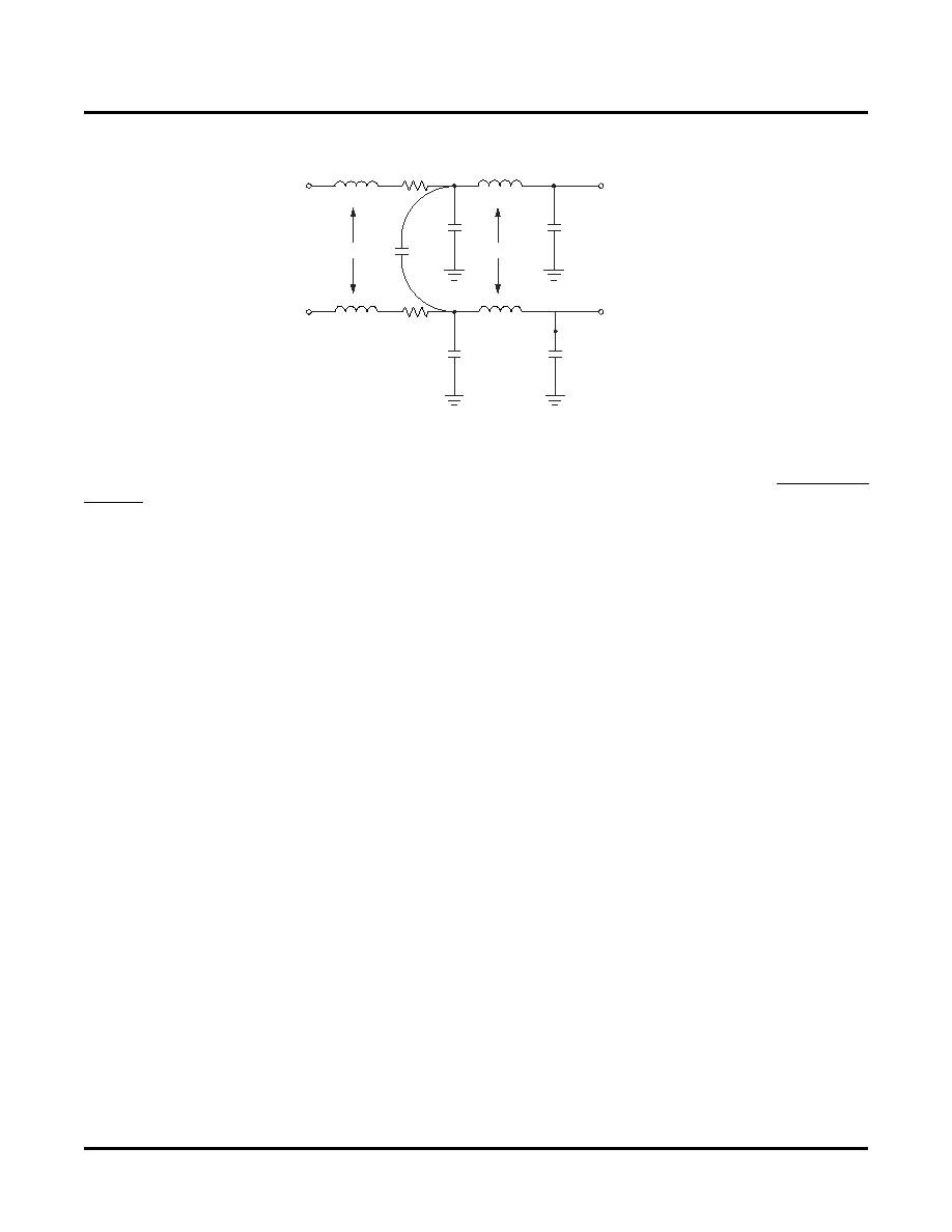
Lattice Semiconductor
ORCA ORT42G5 and ORT82G5 Data Sheet
117
Figure 41. Package Parasitics
Package Outline Drawings
Package Outline Drawings for the 484 ball PBGAM used for the ORT42G5 and 680 ball PBGAM used for the
ORT82G5 are available at the Package Diagrams section of the Lattice Semiconductor web site at www.lattices-
emi.com.
PAD N
Board Pads
C
M
C
1
L
SW
R
W
L
SL
L
MW
C
2
C
1
L
ML
C
2
PAD N + 1
L
SW
R
W
L
SL
Circuit
Pad N+1
Pad N
Package
Pads

Lattice Semiconductor
ORCA ORT42G5 and ORT82G5 Data Sheet
118
Ordering Information
Table 47. Device Type Options
Table 48. Commercial Ordering Information
1
Table 49. Industrial Ordering Information
1
Device
Voltage
ORT42G5
1.5 V internal
3.3 V/2.5 V/1.8 V/ 1.5 V I/O
ORT82G5
1.5 V internal
3.3 V/2.5 V/1.8 V/ 1.5 V I/O
Device Family
Part Number
Speed
Grade
Package
Type
Ball Count
Grade
ORT42G5
ORT42G5-3BM484C
3
PBGAM
484
C
ORT42G5-2BM484C
2
PBGAM
484
C
ORT42G5-1BM484C
1
PBGAM
484
C
ORT82G5
ORT82G5-3BM680C
3
PBGAM
680
C
ORT82G5-2BM680C
2
PBGAM
680
C
ORT82G5-1BM680C
1
PBGAM
680
C
Device Family
Part Number
Speed
Grade
Package
Type
Ball Count
Grade
ORT42G5
ORT42G5-2BM484I
2
PBGAM
484
I
ORT42G5-1BM484I
1
PBGAM
484
I
ORT82G5
ORT82G5-2BM680I
2
PBGAM
680
I
ORT82G5-1BM680I
1
PBGAM
680
I
1. For all but the slowest commercial speed grade, the speed grades on these devices are dual marked. For example, the
commercial speed grade -2XXXXXC is also marked with the industrial grade -1XXXXXI. The commercial grade is always
one speed grade faster than the associated dual mark industrial grade. The slowest commercial speed grade is marked
as commercial grade only.
Device Family
ORT42G5 = 4 SERDES Channels
ORT82G5 = 8 SERDES Channels
ORTX2G5 ≠ X
X
XX
XXX
Speed Grade
Package
BM = Fine-Pitch Plastic Ball Grid Array
(PBGAM)
Grade
C = Commercial
I = Industrial
Ball Count
484
680 (with an embedded
heat spreader)